 Open Access Article
 This Open Access Article is licensed under a Creative Commons Attribution-Non Commercial 3.0 Unported Licence
Dielectrophoretic immobilisation of antibodies on microelectrode arrays
Saskia
Otto
a,
Udo
Kaletta
b,
Frank F.
Bier
a,
Christian
Wenger
b and
Ralph
Hölzel
*a
aFraunhofer Institute for Biomedical Engineering (IBMT), Branch Potsdam-Golm, 14476 Potsdam, Germany. E-mail: ralph.hoelzel@ibmt.fraunhofer.de
bIHP GmbH - Leibniz Institute for Innovative Microelectronics, 15236 Frankfurt/Oder, Germany
First published on 9th December 2013
Abstract
A silicon based chip device with a regular array of more than 100![[thin space (1/6-em)]](https://www.rsc.org/images/entities/char_2009.gif) 000 cylindrical sub-microelectrodes has been developed for the dielectrophoretic (DEP) manipulation of nanoparticles and molecules in solution. It was fabricated by a standard CMOS (complementary metal oxide semiconductor) compatible process. The distribution of the electrical field gradient was calculated to predict the applicability of the setup. Heating due to field application was determined microscopically using a temperature sensitive fluorescent dye. Depending on voltage and frequency, temperature increase was found to be compatible with protein function. Successful field controlled immobilisation of biomolecules from solution was demonstrated with the autofluorescent protein R-phycoerythrin (RPE) and with fluorescently labelled IgG antibodies. Biological activity after DEP application was proven by immobilisation of an anti-RPE antibody and subsequent binding of RPE. These results demonstrate that the developed chip system allows the directed immobilisation of proteins onto microelectrodes by dielectrophoresis without the need for any chemical modification and that protein function is preserved. Being based on standard lithographical methods, further miniaturisation and on-chip integration of electronics towards a multiparameter single cell analysis system appear near at hand.
000 cylindrical sub-microelectrodes has been developed for the dielectrophoretic (DEP) manipulation of nanoparticles and molecules in solution. It was fabricated by a standard CMOS (complementary metal oxide semiconductor) compatible process. The distribution of the electrical field gradient was calculated to predict the applicability of the setup. Heating due to field application was determined microscopically using a temperature sensitive fluorescent dye. Depending on voltage and frequency, temperature increase was found to be compatible with protein function. Successful field controlled immobilisation of biomolecules from solution was demonstrated with the autofluorescent protein R-phycoerythrin (RPE) and with fluorescently labelled IgG antibodies. Biological activity after DEP application was proven by immobilisation of an anti-RPE antibody and subsequent binding of RPE. These results demonstrate that the developed chip system allows the directed immobilisation of proteins onto microelectrodes by dielectrophoresis without the need for any chemical modification and that protein function is preserved. Being based on standard lithographical methods, further miniaturisation and on-chip integration of electronics towards a multiparameter single cell analysis system appear near at hand.
Introduction
Spatial manipulation of suspended objects is a principal task of lab-on-a-chip systems. Well established is the application of inhomogeneous electric fields for sorting, concentrating and characterising living cells by dielectrophoresis (DEP).1–6 Smaller objects like metallic nanoparticles7 and carbon nanotubes8,9 can also be handled. However, with decreasing particle size, Brownian motion and electrohydrodynamic effects increasingly interfere with dielectrophoretic action.10 Accordingly, the number of reports on the successful DEP manipulation of molecules is limited.11–14 Washizu and co-workers were the first to prove DEP action on DNA and proteins.15 Hölzel et al.16 demonstrated DEP manipulation of single protein molecules. Most studies on protein dielectrophoresis employ insulating posts and voltages of several hundred volts to produce the required electric field gradients.14,17,18 Immobilisation of proteins directly onto surfaces has been demonstrated by only a few groups. They applied alternating current (AC) fields in the kHz and MHz range at voltages of about 10 V.15,16,19,20 Depending on field strength, either temporary or permanent immobilisation could be achieved. Still, very few studies have demonstrated that the original protein function is maintained in the course of DEP application. There are only two DEP studies in which the preservation of fluorescence function of autofluorescent proteins has been reported.16,21The problems arising from high voltages and electrohydrodynamic effects can be solved by the use of micro- and nanoelectrodes.16,22,23 However, this usually has called for expensive production techniques like direct-writing electron beam lithography9,16,22 and has hindered a widespread application of molecular dielectrophoresis. The employment of cost-effective fabrication techniques like standard CMOS processes would be highly desirable, since it would allow a simple on-chip integration of fluidics, sensing and signal processing.
In the work presented here, a standard CMOS compatible process has been optimised for the fabrication of regular arrays of more than 100000 sub-microelectrodes with edge curvatures in the nanometre range. Field distributions have been computed and temperature changes have been monitored by confocal microscopy. For the first time, antibodies have been immobilised by DEP and their function has been tested. It could be demonstrated that the antibodies' capability to bind to their specific target is still preserved after DEP immobilisation.
Results and discussion
Field simulation
The dielectrophoretic force, FDEP, can be calculated from FDEP = 2πεmr3Re[f*CM]|grad|E|2| with εm being the medium permittivity, r being the particle radius, Re[f*CM] being the real part of the Clausius–Mossotti factor and grad|E|2 being the gradient of the square of the electric field strength.14,24,25 The Clausius–Mossotti factor is a measure of the particle's polarisability with f*CM = (ε*p − ε*m)/(ε*p + 2ε*m), ε*p and ε*m being the complex permittivities of particle and medium, respectively. From this follows that for the dielectrophoretic manipulation of very small objects like nanoparticles and molecules, one has to take into account that FDEP decreases very fast, i.e. with the cube of the particle radius. At the same time, the influence of Brownian motion increases.10 This can be balanced by increasing the applied voltage and, hence, increased E and grad|E|2.However, this also leads to an increase in side effects like heating and electrohydrodynamic forces that seriously interfere with the envisaged purpose.26,27 Therefore, E is often increased by narrowing the mutual electrode distance down to a few micrometres27,28 or even to the nanometre range.9,16,22,23 In the present setup with the counter electrode placed above the actual chip surface on a spacer, such a distance would be quite difficult to achieve. Therefore, we first simulated the electrical field distribution for such a regular array of metal cylinders immersed in an insulating oxide layer (Fig. 1) assuming the ITO counter electrode to be 100 μm above the array plane. As expected, both field strength and field gradient are maximal at the cylinder's rim. With a potential difference between top electrode and pin electrodes of 1 V, the maximum value for the field gradient is about 1015 V2 m−3. For comparison, some field simulation data for protein DEP can be found in the literature. Using planar electrodes, Asokan et al.29 successfully immobilised actin filaments. Taking into account the differences in applied voltage and electrode distance, their data lead to 1016 V2 m−3 for 1 V potential difference. From a study on DEP manipulation of RNA by Giraud et al.,30 a value of around 1016 V2 m−3 also follows. From an earlier study on dielectrophoresis of R-phycoerythrin between planar triangular electrodes,16 we obtain values of about 1015 V2 m−3 at the electrode tips, again after correcting for differences in voltage and electrode distance. In a successful insulator based DEP approach on IgG molecules, Nakano et al.18 calculated field gradients exceeding 1017 V2 m−3 at 0.3 MV m−1 field strength, which translate to values around 3 × 10¹⁴ V2 m−3. Taken together, the field gradients of quite different electrode geometries for successful protein DEP span two orders of magnitude from about 3 × 10¹⁴ V2 m−3 to 2 × 10¹⁶ V2 m−3 with the present setup being covered. Taking into account the voltages applied in these studies, for a top electrode being 100 μm above the needle array, voltages between 5 Vrms and 20 Vrms are expected to be suitable.
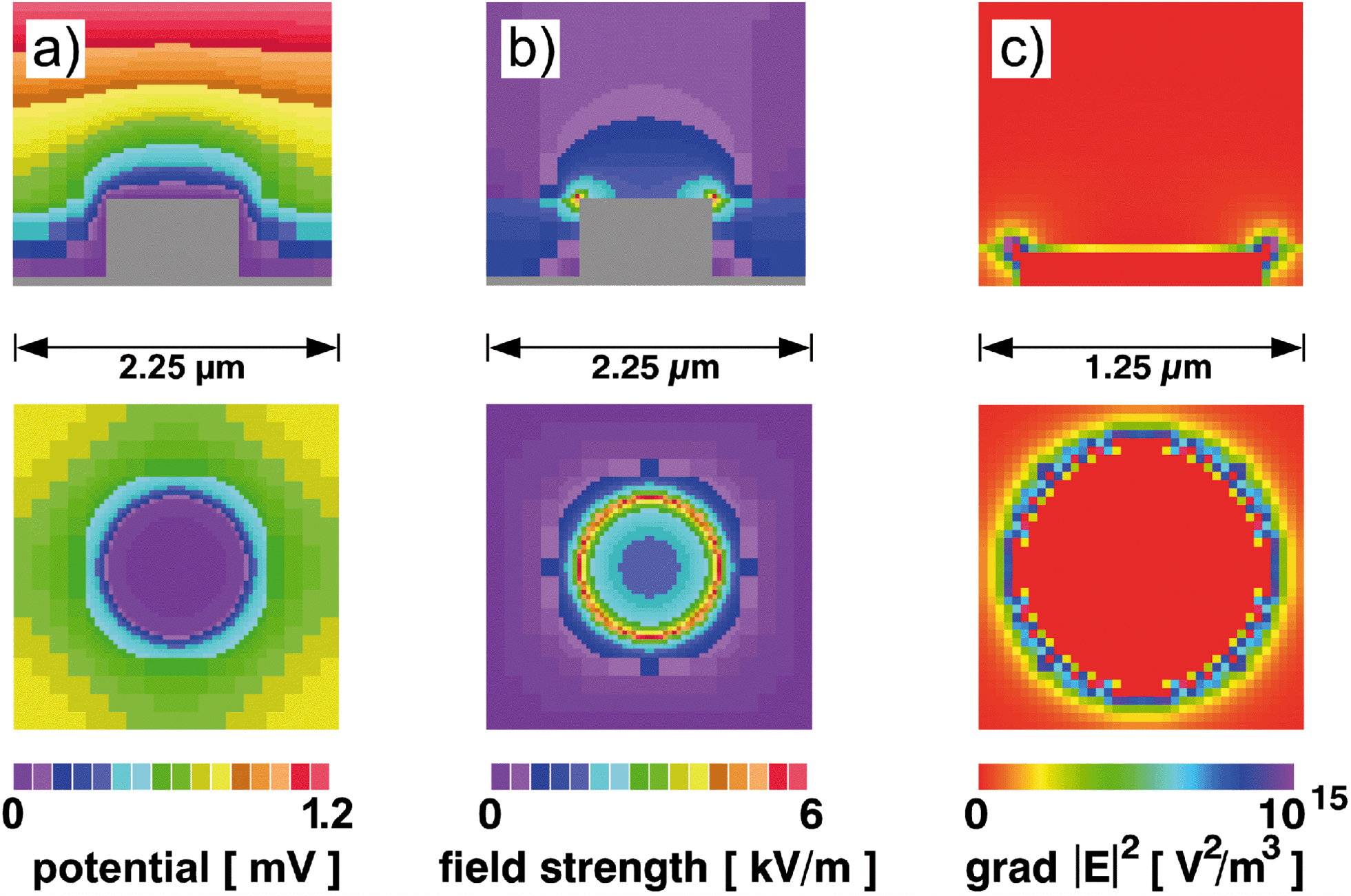 | ||
| Fig. 1 Calculated field distribution around an electrode pin. a) Electrical potential, U, b) field strength, |E|, c) absolute value of the gradient of the squared field strength, |grad|E|2|. Upper row: side view, lower row: top view. | ||
The main difference between the present electrode geometry and that of the widespread co-planar systems with both electrodes in the same plane16,22,23,27,31,32 is the placement of the counter electrode which is quite distant from the high field gradient region. As a consequence, the electric field vector is primarily oriented orthogonal to the surface in contrast to the coplanar structures which have a strong tangential field component. This follows from qualitative physical reasons as well as from our own field simulations comparing both electrode types (data not shown). This tangential field can lead to AC electroosmotic fluid flow33 which interferes with DEP accumulation. Therefore, the presented needle array arrangement is expected to be more suitable for nanoparticle and molecular dielectrophoresis than coplanar IDE structures.
Temperature measurement
The expected main cause of deterioration of antibody function in the course of dielectrophoretic manipulation is a rise in temperature of the sample solution. Reliable determination of the temperature within such small aqueous volumes of about 1 μl is usually performed by optical means.34 The most accurate method is based on the temperature dependent fluorescence of certain dyes. Seger-Sauli et al.35 used Rhodamine B to measure temperatures in microfluidic DEP systems. They report a loss in fluorescence intensity with rising temperature at −1.2% K−1 for a 1 mM dye solution. We therefore simulated a typical DEP experiment by filling the chamber with an aqueous 1 mM Rhodamine B solution, and varied the voltage at two frequencies. 100 kHz and 500 kHz were chosen because in earlier experiments the intrinsically fluorescent protein R-phycoerythrin had responded well in this frequency range. Fig. 2 shows the changes in fluorescence intensity and the corresponding temperature changes for different applied voltages over a period of 15 min. The observed temperature increase reached equilibrium after 2 to 5 minutes in an exponential manner. | ||
| Fig. 2 Temperature increase during field application. Decrease in fluorescence intensity of Rhodamine B (left scale) is a measure of temperature increase (right scale, note the inverted scale). | ||
From the values at 500 kHz, a nearly square dependence on voltage can be deduced. This corresponds to a nearly linear correlation with electrical power which is quite reasonable35 and which has also been found by Jaeger et al.34 Interestingly, a change in frequency by a factor of 5 leads to a 3.5-fold increase in temperature, whilst from the data of Jaeger et al.34 only a two-fold temperature rise follows for a nearly 200-fold frequency change from 36 kHz to 6.8 MHz. This strong frequency dependence could be explained by a series capacitance of the system although its origin is rather unclear. It might be a consequence of electrode polarisation; however, this effect is usually significant at much lower frequencies.36 Another source of series capacitance could be the capacitor that is formed by the conductive glass slide and the underlying silver paint which are only loosely connected (Fig. 6). Frequency dependent heating due to orientational polarisation37 can be excluded, since a rough calculation for 500 kHz yields less than 0.1% of the temperature rise of that due to Joule heating at 1 μS cm−1. The determined temperature increase of up to nearly 60 K appears rather large. However, Seger-Sauli et al.35 report heating in dielectrophoretic systems by 30 K at 8 Vrms, corresponding well with our data. For estimating the dissipated power, one can assume a solution volume on top of the electrode array of 1 mm × 1 mm × 0.1 mm, a conductivity of 1 μS cm−1 and a voltage of 21 Vrms resulting in a power of 0.44 mW. Taking into account the specific heat capacitance of water, one obtains a temperature rise of about 1 K per minute. This is in very good accordance with the measured initial temperature change of 35 K within the first 30 s of field application. Still, the interaction of the electric field with the temperature sensitive dye has been neglected here as has been in the literature34,35 and, moreover, might be frequency dependent. The dye is expected to increase solution conductivity and, hence, Joule heating, which should result in an overestimation of the actual temperature rise.
Dielectrophoresis of proteins
R-phycoerythrin
In order to test the needle electrode array's suitability for protein DEP, the autofluorescent protein R-phycoerythrin (RPE) was chosen for its strong fluorescence yield. It has a disklike shape with a diameter of 11 nm and a thickness of 6 nm at a molecular mass of 240 kDa.38 The measuring chamber was filled with a 1 μg ml−1 solution corresponding to about 2.5 molecules per μm3. This led to an evenly distributed fluorescence in the field of view before field application. Switching on the field at 500 kHz and 18 Vrms led to clearing of the area between the electrode pins and to a continuous increase of fluorescence intensity at the electrode over 5 minutes (Fig. 3a). Longer field application typically led to no further increase in fluorescence. Closer inspection of individual electrodes showed that the RPE molecules were collected in several experiments at the electrode cylinders' rim in good agreement with the field simulations. However, other experiments exhibited fluorescence on the entire cylinder surface (Fig. 3) or just in the centre of the cylinders' surface (Fig. 4, inset). These findings presumably are caused by differing properties of the electrode surface. Freshly prepared electrodes sometimes show a central elevation (Fig. 5g) that could act as an additional source of inhomogeneity. Moreover, atomic force microscopy of used electrodes (data not shown) often reveals a hollow at the electrode's position possibly caused by electrolytic etching that would change the field distribution and, hence, protein distribution. | ||
| Fig. 3 a) Dielectrophoretic immobilisation of the autofluorescent protein R-phycoerythrin (RPE). Fluorescence micrograph after 5 min field application at 500 kHz, 14 Vrms. b) Dielectrophoretic immobilisation of a fluorescently labelled IgG antibody. Fluorescence micrograph after 30 s field application at 100 kHz, 14 Vrms. Scale bars 50 μm. | ||
 | ||
| Fig. 4 Dielectrophoretic immobilisation of an anti-RPE antibody and subsequent incubation with the antigen RPE. Field application for 20 min at 100 kHz, 18 Vrms. Superposition of a reflection image of the electrode array (monochrome greyscale image presented in violet) and a fluorescence micrograph taken in the RPE channel (monochrome greyscale image presented in yellow). | ||
 | ||
| Fig. 5 Fabrication process of the microelectrode array. a) Metal deposition; b) SiO2 deposition, chemical mechanical polishing (CMP) and etching of via trenches; c) filling of via trenches with tungsten and CMP; d) 3D cutaway view; e) confocal reflection micrograph of a part of the electrode array, scale bar 50 μm; f) detailed view of e), scale bar 2 μm; g) scanning electron micrograph of a single tungsten electrode embedded in SiO2, cross section, scale bar 500 nm. | ||
The actual molecular mechanism responsible for the permanent immobilisation of proteins is not yet clear. Dielectrophoresis of bovine serum albumin has been reported to show a transition from temporal to permanent immobilisation above a certain field strength.20 Therefore, we assume that above a certain field threshold, dielectrophoretic attraction of the hydrated macromolecule leads to direct contact of the protein with the electrode surface. By this, most of the hydration layer is shifted aside, resulting in hydrophobic interaction taking place between protein and surface. Besides, the composition, roughness and porosity of the electrode on the nanoscale have to be considered. In the present system, the electrode material tungsten is covered with a layer of several tungsten oxides with different oxidation states.
Antibodies
For testing and optimisation of the dielectrophoretic immobilisation of antibodies, polyclonal goat anti-human IgG was used. It was fluorescently labelled with the dye DY-634 by covalent coupling to its amino groups and diluted to a final concentration of 4.2 nM, i.e. 2.5 molecules per μm3. After field application at 100 kHz and 14 Vrms, collection was clearly discernible at the electrodes within a few seconds (Fig. 3b). Switching off the field resulted in a slight loss in fluorescence of less than 10%, indicating that some of the molecules had been immobilised only temporarily.Only few data on the dielectrophoretic action on antibodies can be found in the literature. Kawabata and Washizu39 retracted IgM antibodies (900 kDa) in a DEP chromatography device based on interdigitated electrodes at a field frequency of 1 MHz and determined its response by measurement of the bulk fluorescence at the outlet. In an electrodeless DEP approach using direct current (DC), Clarke et al.40 increased the concentration of IgG by a factor of 300 at the tip of a glass capillary. This principle was developed further by Nakano et al.18 towards a microstructured device where IgG was trapped at insulating field constrictions in a DC field. In a similar approach, Qiao et al.19 trapped IgG in holes in an electrically insulating membrane using DC fields. Whilst these studies were aimed at a concentration of molecules in the bulk, the present work demonstrates for the first time that it is possible to immobilise antibodies on surfaces by DEP permanently. These surfaces can be the active region of micrometre sized or even smaller electronic biosensors. The local accumulation allows rather low initial antibody concentrations in the volume. Above that, no chemical modification of the antibodies is needed which simplifies the coating process and reduces the risk of unwanted modification of the binding region.
Whilst there are quite a number of publications on the dielectrophoretic manipulation of proteins, no efforts seem to have been made to test whether this actually leaves protein function intact. Only in two studies does the evident concentration of the autofluorescent proteins YFP (yellow fluorescing protein)21 and RPE16 prove that the activity of the fluorescing subunits is at least not severely affected. In order to test antibody function after DEP application, we therefore applied the DEP protocol that had been developed for dye labelled antibodies to unlabelled ones that are directed against RPE. 2.5 μl of a 9 nM solution of anti-RPE-IgG1 (150 kDa) antibodies, that is a concentration of about 5 molecules per μm3, were placed onto the electrode array. A signal of 100 kHz at 18 Vrms was applied for 20 minutes. After careful rinsing with water and drying with an air stream, the array was incubated with 2.5 μl of a 1 μg ml−1 RPE solution for 20 minutes. Again, the chip was rinsed and air dried, and then observed under the microscope (Fig. 4). For a proper localisation of fluorescing spots, both fluorescence images and brightfield images in reflection mode were acquired and combined. Clearly, fluorescence was completely localised at the electrodes. In the field of view, which comprises around 3000 electrode pins, most electrodes were covered with RPE. Still, outside the field of view of Fig. 4, there was a gradient in coverage of the electrodes with the brightest fluorescence at the array's periphery. This is interpreted to be a result of – presumably electrothermal – fluid flow10 directed from outside the array towards its centre. Proteins carried with this flow will be attracted by the electrodes at the array's periphery before they can reach the central region. Consequently, a more even distribution is expected to be attainable at higher antibody concentrations and a more elaborate DEP protocol. The inset of Fig. 4 suggests a more even distribution of RPE on each electrode cylinder than attained by the direct DEP immobilisation of RPE (Fig. 3a). This was achieved by reducing the field frequency from 500 kHz to 100 kHz, increasing the duration of field application from 5 min to 20 min and increasing the protein concentration by 25%. Still, the theoretical optical resolution of the used objective at 530 nm emission wavelength is 0.45 μm. This is just half the electrode diameter and therefore limits possible conclusions about local protein distribution. A more systematic optimisation of immobilisation parameters calls for higher resolution which could be achieved using better objectives or applying scanning force microscopy. In a control experiment without antibodies and field application, incubation for 20 min in RPE solution alone did not lead to any fluorescence changes at the electrode.
Materials and methods
Chemicals
If not otherwise stated, all solutions were prepared from ultra-pure water with a conductivity of not more than 2 μS cm−1. Rhodamine B (Sigma-Aldrich, München, Germany) was diluted to 1 mM. The intrinsically fluorescent protein R-phycoerythrin (RPE, MW 240000) was purchased from Sigma-Aldrich as dry powder, dissolved to 1 mg ml−1 in water and kept in aliquots at −80 °C. These were later diluted for use, typically 1:1000, i.e. to 1 μg ml−1. Mouse IgG1 antibodies directed against phycoerythrin (Biolegend, Fell, Germany) were dissolved to 1.3 μg ml−1. Goat anti-human antibodies (Bethyl, Montgomery, USA) were labelled with the fluorescent dye Dy-634 (Dyomics, Jena, Germany) using its NHS ester and diluted to 0.8 μg ml−1.
Electrode preparation
Regular arrays of cylindrical electrodes were prepared in a standard 0.25 μm microfabrication process (Fig. 5a–d) which is compatible with CMOS (complementary metal oxide semiconductor) production techniques. The process flow started with the deposition of a metal stack consisting of TiN–Ti–Al–Ti–TiN directly grown on silicon (Fig. 5a). The SiO2 layer was deposited on top of this metal stack and the holes for the tungsten pins were etched by a reactive ion etching (RIE) process into the SiO2 film (Fig. 5b) down to the metal layer. The holes were filled with tungsten, giving direct contact to the metal stack, and the surface was planarised by chemical mechanical polishing (CMP, Fig. 5c).This resulted in a regular orthogonal array (Fig. 5d, e) of more than 100000 cylindrical tungsten pins embedded in an amorphous SiO2 matrix. The array covered 1 mm2 with a mutual electrode distance of 2.1 μm (Fig. 5f). Tungsten was chosen for its good chemical resistance and biocompatibility as it is widely used, e.g., in electrophysiology. Care was taken to achieve complete filling of the vias, resulting in tungsten cylinders of 900 nm diameter and 500 nm height. Due to the polishing process, the actual radius of curvature of the cylinders' rim was not more than 30 nm as revealed by scanning electron microscopy of a vertical cut through the pin (Fig. 5g).
Measuring chamber
The silicon wafer was cut to 1 cm2 sized squares with the 1 mm2 electrode array positioned in the centre of each. The chip was mounted onto a glass microscope slide with electrically conductive paint (Conrad, Wernberg, Germany) which also served as a conductive line to the connector (Fig. 6a, b). The sample was confined by a circular spacer ring of 80 μm thickness, which had been cut out from a polyester laminating film. With its lower side coated by a thin polyethylene layer, it was attached to the chip by melting this layer by heating to around 80 °C. The sample volume was sealed airtight by a thin layer of vaseline (Hagner, Freudenstadt, Germany) between spacer and cover glass. The cover glass served as the counter electrode to the tungsten pin array. It was prepared from indium tin oxide (ITO) coated slides (SPI Supplies, West Chester, USA; 30–60 Ω) which were cut to 10 mm squares. Proper contact to the ITO layer was achieved with a small phosphor bronze receptacle (TE Connectivity, Schaffhausen, Switzerland) that had been pressed flat to fit tightly to the ITO glass slide. For short experiments when evaporation was not a problem, vaseline was omitted. In this case, the electrical contact to the ITO layer was achieved by a thin film of conductive paint on the spacer surface and by placing the cover slide directly onto this film. | ||
| Fig. 6 a) Measuring chamber. The electrode array is attached to the microscope slide and contacted by a silver paint layer. An ITO slide serves as the top electrode and is contacted by a bronze receptacle. The sample volume is sealed with a polyester ring and vaseline. b) Experimental setup. Electrodes are powered by a function generator and amplifier. Voltage and frequency are monitored by using a voltmeter and a counter, respectively. Micrographs are acquired by using a CCD camera. | ||
Experimental system
The complete system for dielectrophoretic experiments is shown in Fig. 6b. Most experiments were performed using an upright epifluorescence microscope (BX51, Olympus, Hamburg, Germany) with different filter sets for RPE (BP460-495, DM505, BA510-550, U-MWIBA3, Olympus) and for DY-634 (ET 620/60, T660lpxr, ET700/75, Chroma, Bellows Falls, USA). Objectives were UPlanFL N 40×/0.75 and LUCPlanFL N 60×/0.70 (Olympus). Images were acquired with a cooled CCD camera (F-View II, SIS, Münster, Germany) controlled by the software cellM (Olympus). A shutter in the excitation path helped to minimize bleaching of the samples and was also computer controlled. For fluorescence based temperature measurements, a confocal laser scanning microscope (LSM510, Zeiss, Jena, Germany) was used at 543 nm with a dichroic mirror HFT488/543, a long pass filter LP585 and a 10× objective.AC signals were delivered by a function generator (Model 193, Wavetek, San Diego, USA) followed by a wide band power amplifier (TOE 7606, Toellner, Herdecke, Germany) and a mechanical switch. All cables were coaxial except the last 10 cm close to the electrode chip, which were prepared from a flexible two-wire flat cable in order to minimize mechanical impact on electrode position. Signal frequency was monitored with a counter (Voltcraft 7202, Conrad, Wernberg, Germany), and amplitudes were measured with a voltmeter (DMM 177, Keithley, Cleveland, USA) equipped with a demodulator probe (TT-DE 112, Testec, Frankfurt, Germany).
Field simulations
The three-dimensional electric field distribution was calculated using the finite element program Maze (Field Precision, Albuquerque, USA). From the resulting potential distribution, U(x, y, z), the square of the field strength |E(x, y, z)|2 was calculated using the computer algebra system Maple 10 (Maplesoft, Waterloo, Canada). From this, the absolute value of the field gradient, grad|E|2, was calculated, giving a measure of the dielectrophoretic force.Conclusion
It has been demonstrated for the first time that dielectrophoresis can be used as a simple means to immobilise proteins on conducting surfaces and that protein function is retained in the course of field application. Fabrication of the electrodes by a standard CMOS compatible process implies that electronic circuitry for data acquisition and processing can be readily integrated into the chip. In addition, each electrode could be individually activated, rendering a different functionalisation for each electrode quite simple. This could be exploited for the production of very compact multi-parameter lab-on-a-chip systems as well as of high-density protein and DNA microarrays. Owing to the relatively simple electrode layout, fabrication using printed electronics also appears as an option leading to cost-effective disposable systems.Acknowledgements
We thank E. Ermilova and E.-M. Laux for helpful discussions and D. Michel for his assistance with protein labelling. Financial support from the European Regional Development Fund and from the German state Brandenburg within the project Terasens is gratefully acknowledged.References
- R. Pethig and G. H. Markx, Trends Biotechnol., 1997, 15, 426–432 CrossRef CAS.
- P. R. C. Gascoyne and J. Vykoukal, Electrophoresis, 2002, 23, 1973–1983 CrossRef CAS.
- M. P. Hughes, Electrophoresis, 2002, 23, 2569–2582 CrossRef CAS.
- X. Y. Hu, P. H. Bessette, J. R. Qian, C. D. Meinhart, P. S. Daugherty and H. T. Soh, Proc. Natl. Acad. Sci. U. S. A., 2005, 102, 15757–15761 CrossRef CAS PubMed.
- H. Moncada-Hernandez and B. H. Lapizco-Encinas, Anal. Bioanal. Chem., 2010, 396, 1805–1816 CrossRef CAS PubMed.
- F. S. O. Fritzsch, K. Rosenthal, A. Kampert, S. Howitz, C. Dusny, L. M. Blank and A. Schmid, Lab Chip, 2013, 13, 397–408 RSC.
- K. D. Hermanson, S. O. Lumsdon, J. P. Williams, E. W. Kaler and O. D. Velev, Science, 2001, 294, 1082–1086 CrossRef CAS PubMed.
- R. Krupke, F. Hennrich, H. v. Löhneysen and M. M. Kappes, Science, 2003, 301, 344–347 CrossRef CAS PubMed.
- C. W. Marquardt, S. Grunder, A. Blaszczyk, S. Dehm, F. Hennrich, H. v. Löhneysen, M. Mayor and R. Krupke, Nat. Nanotechnol., 2010, 5, 863–867 CrossRef CAS PubMed.
- A. Castellanos, A. Ramos, A. Gonzalez, N. G. Green and H. Morgan, J. Phys. D: Appl. Phys., 2003, 36, 2584–2597 CrossRef CAS.
- R. Hölzel and F. F. Bier, IEE Proc.: Nanobiotechnol., 2003, 150, 47–53 CrossRef.
- B. H. Lapizco-Encinas and M. Rito-Palomares, Electrophoresis, 2007, 28, 4521–4538 CrossRef CAS PubMed.
- R. Hölzel, IET Nanobiotechnol., 2009, 3, 28–45 CrossRef PubMed.
- A. Nakano and A. Ros, Electrophoresis, 2013, 34, 1085–1096 CrossRef CAS PubMed.
- M. Washizu, S. Suzuki, O. Kurosawa, T. Nishizaka and T. Shinohara, IEEE Trans. Ind. Appl., 1994, 30, 835–843 CrossRef CAS.
- R. Hölzel, N. Calander, Z. Chiragwandi, M. Willander and F. F. Bier, Phys. Rev. Lett., 2005, 95, 128102 CrossRef.
- C.-F. Chou, J. O. Tegenfeldt, O. Bakajin, S. S. Chan, E. C. Cox, N. Darnton, T. Duke, A. Nakano, T.-C. Chao, F. Camacho-Alanis and A. Ros, Electrophoresis, 2011, 32, 2314–2322 Search PubMed.
- A. Nakano, T.-C. Chao, F. Camacho-Alanis and A. Ros, Electrophoresis, 2011, 32, 2314–2322 CAS.
- W. Qiao, G. Cho and Y.-H. Lo, Lab Chip, 2011, 11, 1074–1080 RSC.
- T. Yamamoto and T. Fujii, Nanotechnology, 2007, 18, 495503 CrossRef PubMed.
- R. W. Clarke, J. D. Piper, L. Ying and D. Klenerman, Phys. Rev. Lett., 2007, 98, 198102 CrossRef.
- S. Tuukkanen, A. Kuzyk, J. J. Toppari, H. Häkkinen, V. P. Hytönen, E. Niskanen, M. Rinkiö and P. Törmä, Nanotechnology, 2007, 18, 295204 CrossRef.
- C. Leiterer, S. Berg, A. Eskelinen, A. Csaki, M. Urban, P. Törmä and W. Fritzsche, Sens. Actuators, B, 2013, 176, 368–373 CrossRef CAS PubMed.
- T. B. Jones, IEEE Eng. Med. Biol. Mag., 2003, 22, 33–42 CrossRef.
- R. Pethig, Biomicrofluidics, 2010, 4, 022811 CrossRef PubMed.
- N. G. Green, A. Ramos, A. Gonzalez, H. Morgan and A. Castellanos, Phys. Rev. E: Stat. Phys., Plasmas, Fluids, Relat. Interdiscip. Top., 2002, 66, 026305 CrossRef CAS.
- S. Stanke, F. F. Bier and R. Hölzel, Electrophoresis, 2011, 32, 2448–2455 CrossRef CAS PubMed.
- A. Henning, F. F. Bier and R. Hölzel, Biomicrofluidics, 2010, 4, 022803 CrossRef PubMed.
- S. B. Asokan, L. Jawerth, R. L. Carroll, R. E. Cheney, S. Washburn and R. Superfine, Nano Lett., 2003, 3, 431–437 CrossRef CAS.
- G. Giraud, R. Pethig, H. Schulze, G. Henihan, J. G. Terry, A. Menachery, I. Ciani, D. Corrigan, C. J. Campbell, A. R. Mount, P. Ghazal, A. J. Walton, J. Crain and T. T. Bachmann, Biomicrofluidics, 2011, 5, 024116 Search PubMed.
- F. F. Becker, X.-B. Wang, Y. Huang, R. Pethig, J. Vykoukal and P. R. C. Gascoyne, Proc. Natl. Acad. Sci. U. S. A., 1995, 92, 860–864 CrossRef CAS.
- A. Kuzyk, Electrophoresis, 2011, 32, 2307–2313 CAS.
- A. Ramos, H. Morgan, N. G. Green and A. Castellanos, J. Colloid Interface Sci., 1999, 217, 420–422 CrossRef CAS PubMed.
- M. S. Jaeger, T. Mueller and T. Schnelle, J. Phys. D: Appl. Phys., 2007, 40, 95–105 CrossRef CAS.
- U. Seger-Sauli, M. Panayiotou, S. Schnydrig, M. Jordan and P. Renaud, Electrophoresis, 2005, 26, 2239–2246 CrossRef CAS PubMed.
- V. F. Lvovich, Impedance spectroscopy, Wiley, Hoboken, 2012 Search PubMed.
- R. Pethig, Dielectric and electronic properties of biological materials, John Wiley, Chichester, 1979 Search PubMed.
- M. Goulian and S. M. Simon, Biophys. J., 2000, 79, 2188–2198 CrossRef CAS.
- T. Kawabata and M. Washizu, IEEE Trans. Ind. Appl., 2001, 37, 1625–1633 CrossRef CAS.
- R. W. Clarke, S. S. White, D. Zhou, L. Ying and D. Klenerman, Angew. Chem., 2005, 117, 3813–3816 CrossRef.
| This journal is © The Royal Society of Chemistry 2014 |