 Open Access Article
 This Open Access Article is licensed under a
 Creative Commons Attribution 3.0 Unported Licence
Characterization and simulation of electrolyte-gated organic field-effect transistors
Katharina
Melzer
*,
Marcel
Brändlein
,
Bogdan
Popescu
,
Dan
Popescu
,
Paolo
Lugli
and
Giuseppe
Scarpa
Institute for Nanoelectronics, TU München, Arcisstrasse 21, 80333 München, Germany. E-mail: katharina.melzer@nano.ei.tum.de
First published on 2nd June 2014
Abstract
In this work we fabricate and characterize field-effect transistors based on the solution-processable semiconducting polymer poly(3-hexylthiophene) (P3HT). Applying two independent gate potentials to the electrolyte-gated organic field-effect transistor (EGOFET), by using a conventional SiO2 layer as the back-gate dielectric and the electrolyte-gate as the top-gate, allows the measurement of the electrical double layer (EDL) capacitance at the semiconductor–electrolyte interface. We record the transfer curves of the transistor in salt solutions of different concentration by sweeping the bottom gate potential for various constant electrolyte-gate potentials. A change of the electrolyte-gate potential towards more negative voltages shifts the threshold voltage of the bottom-gate channel towards more positive back-gate potentials, which is directly proportional to the capacitive coupling factor. By operating the EGOFET in the dual-gate mode, we can prove the dependency of the EDL capacitance on the molarity of the electrolyte according to the Debye–Hückel theory, and additionally show the difference between a polarizable and non-polarizable electrolyte-gate electrode. With the experimentally obtained values for the EDL capacitance at the semiconductor–electrolyte interface we can model the electrolyte-gate transfer characteristics of the P3HT OTFT.
1 Introduction
Organic thin-film transistors (OTFTs) have been explored for various sensing applications in recent years due to their easy and low-cost fabrication (for recent reviews refer to1–3 and references therein). In particular, the semiconducting polymer poly(3-hexylthiophene) (P3HT) is well-established as the active semiconducting component in OTFTs for biosensing applications4–9 due to several key features offered by the material: its outstanding biocompatibility,10 its solution processability and subsequent applicability in large-scale, flexible and cost-effective electronics, and its relatively high mobility.11,12In organic thin-film transistors, in general a thin film of an organic semiconducting material is utilized as the active layer. Two contacts, the source and drain electrodes, which are in direct contact with the semiconducting material, are used to apply the source–drain voltage and to measure the current flowing between them through the organic semiconducting channel. As the third electrode, the gate electrode is used to control the number of charge carriers, in p-type material holes, in the semiconducting channel at the interface between the semiconductor and the gate dielectric through an electric field applied across the insulating gate dielectric. Therefore one can modulate the source–drain current flowing between the source and drain contacts by applying a given potential to the gate electrode. For a p-type material the transistor is turned “ON” for negative gate voltages, whereas a positive gate bias switches the device “OFF”.13
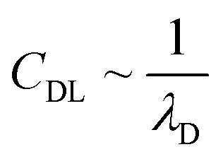
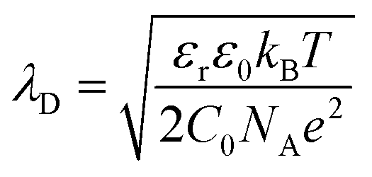
In recent years the usage of solid and liquid electrolytes as gate dielectrics in OTFTs has gained great interest. They display a huge capacitance (CG) compared to the conventional silicon dioxide (SiO2), which is typically in the range of 1–100 μF cm−2, ∼1000 times higher than the one offered by a nm-thick SiO2-layer.1,12,14,15 Especially important in EGOFETs is the formation of an electrical double layer (EDL) at the electrolyte–semiconductor interface as well as the gate electrode–electrolyte interface. At the gate electrode–electrolyte interface the electronic charges close to the electrode surface are compensated by oppositely charged ions in the electrolyte close to the interface. At the electrolyte–semiconductor interface the EDL consists of ions forming the inner Helmholtz plane in the electrolyte and charge carriers in the semiconducting channel. Additionally, at both interfaces, hydrated ions of both charges accumulate and form the outer Helmholtz plane. In the bulk of the electrolyte, the potential stays constant as the diffuse layer of the hydrated positive and negative ions ensures charge neutrality.12,15,16 The charge distribution in an EDL can be described by the Gouy–Chapman–Stern model.17–20 In the case of a flat electrode surface, the electrostatic capacitance of the EDL can be related to the Debye length λD, which defines the distance d between the interface and the outermost layer of ions which is necessary to compensate the gate surface charge fully. The Debye length is inversely proportional to the square root of the ionic strength, according to:
 | (1) |
 | (2) |
Therefore it is of great interest for various sensing applications with EGOFETs to obtain information about how changes to the electrolyte–semiconductor interface, especially to the electrical double layer and its capacitance, influence the transistor characteristics.
In this work we concentrate on the influence of the electrical double-layer capacitance (CDL) and try to gain information about the dependency of CDL on the ionic strength of the electrolyte. We operate the OTFT based on the semiconducting polymer poly(3-hexylthiophene) (P3HT) in the so-called dual-gate mode23 by using both a conventional back-gate as well as an electrolyte-gate as the top-gate. Exploiting the capacitive coupling factor23,24 allows us to extract the double-layer capacitance from several back-gate sweeps with different constant electrolyte-gate potentials. Changing the ionic strength of the aqueous potassium chloride (KCl) solution used as the gate dielectric for the electrolyte-gate gives us the double-layer capacitance as a function of the salt concentration. We demonstrate that the capacitance of the electrical double layer at the semiconductor–electrolyte interface increases with an exponential increase of the ionic strength of the electrolyte. In addition to the electrical characterization of the organic thin-film transistors, we compare the results to theoretical data gained from simulations with a modified drift–diffusion model.
2 Experimental
2.1 Device fabrication
Organic thin-film transistors (OTFTs) were processed using highly p-doped silicon wafers (Si-Mat) as a substrate with a thermally grown 65 nm thick silicon dioxide layer (SiO2) as the conventional gate dielectric. Source and drain electrodes (5 nm Cr as adhesion layer, 40 nm Au) were patterned on top of the oxide layer by a conventional negative optical photolithography process. An interdigitated finger structure (IDES) was used as the electrode structure, with a channel length of 50 μm and a width-to-length ratio of 900. A 1 wt% solution of regioregular poly(3-hexylthiophene) (P3HT, Rieke Metals) in anhydrous 1,2-dichlorobenzene (DCB, VWR) was prepared and stirred for 30 min to obtain a homogeneous solution. The solution was then filtered through a polytetrafluoroethylene (PTFE) syringe filter with a pore size of 200 nm (VWR) and spin-coated (1000 rpm, 90 s) onto the surface of the wafer in a glove box system (N2). After spin-coating, the film was annealed on a hot plate under a nitrogen atmosphere at 150 °C for 20 min. The obtained polymer layer was approximately 50 to 70 nm thick. Atomic force microscopy (AFM, Jeol, JSPM-5200) measurements yielded an Rq value of 3.4 nm, which is a measure for the surface roughness of the polymeric film, and a peak-to-valley distance of about 22 nm.2.2 Electrical characterization
Transfer characteristics (IDvs. VG) and output characteristics (IDvs. VDS) of the devices were recorded using a Keithley 4200-SCS semiconductor parameter analyser system. To operate the transistor in liquid, measurements were performed after mounting the devices in a PDMS flow-chamber, which has a liquid compartment volume of 100 μL. The transfer characteristics of the OTFT were obtained by sweeping either the back-gate potential (VDS = −10 V) or the electrolyte-gate potential (VDS = −0.1 V), while a constant drain voltage VDS was applied. For the back-gate sweep no electrolyte was on top of the semiconducting layer, whereas for the electrolyte-gate sweep the back-gate electrode was left floating. The electrolyte-gate potential was chosen from the relatively small voltage regime between VTgS = +0.6 V and VTgS = −0.6 V to avoid any water hydrolysis or any other electrochemical reaction at the gate electrode or the semiconductor surface.12For the measurement of the electrical double layer capacitance, the potential at the electrolyte-gate electrode, either a Pt wire or a homemade Ag/AgCl electrode, was kept constant while a scan of the back-gate voltage between VBgS = +20 V and VBgS = −7.5 V was performed. The back-gate sweep was recorded for six different electrolyte-gate potentials between VTgS = +0.1 V and VTgS = −0.4 V, whereas the drain voltage was kept constant for each back-gate sweep at VDS = −0.1 V. All characterization measurements were performed in ambient conditions. The electrolyte was exchanged manually using a Gilson pipette. After exchanging the electrolyte the system was left to equilibrate for 5 minutes before the next measurement was started.
2.3 Preparation of electrolytes
The electrical double layer capacitance was characterized using either deionized water (DI-H2O, classified with a resistivity of 18.2 MΩ cm). Potassium chloride solutions were prepared by dissolving 100 mM KCl (≥99.0%, Sigma Aldrich) in DI-H2O and further diluting it with DI-H2O to the desired KCl concentrations.3 Results and discussion
3.1 Device characteristics
The transfer characteristics of the OTFT were obtained by sweeping either the back-gate potential or the electrolyte-gate potential, while a constant drain voltage VDS was applied. For the back-gate sweep no electrolyte was on top of the semiconducting layer, whereas for the electrolyte-gate sweep the back-gate electrode was left floating. Fig. 1(a) shows the source–drain current IDversus the back-gate potential; the drain voltage was kept constant at VDS = −10 V. Fig. 1(b) shows IDversus the electrolyte-gate potential VTgS of the OTFT gated with a Pt electrode in a 10 mM solution of KCl in DI-water as the electrolyte; the drain voltage was kept constant at VDS = −0.1 V. Both transfer curves exhibit typical p-type field-effect characteristics with ON/OFF ratios of around 100. When the OTFT is operated with the conventional silicon dioxide (SiO2, 65 nm, COx = 53.2 nF cm−2) back-gate, the transfer curve reveals a transconductance of gm = 2.4 μS. The transconductance of organic thin-film transistors is usually given by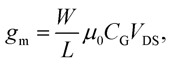 | (3) |
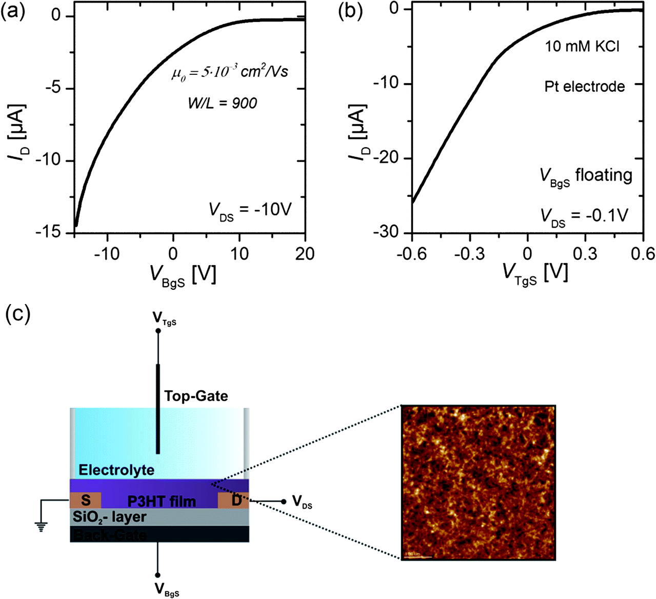 | ||
| Fig. 1 (a) Transfer characteristics of a back-gated P3HT OTFT. (b) Transfer characteristics of an electrolyte-gated P3HT OTFT recorded in a 10 mM KCl solution. A Pt wire was used as the electrolyte-gate electrode. The back-gate electrode was left floating. (c) Schematic representation of a dual-gated P3HT OTFT. A 65 nm thick SiO2-layer was used as the back-gate dielectric, whereas various electrolytes serve as the top-gate dielectric. The magnification shows an AFM scan (scan size 5 μm × 5 μm) of the spin-coated P3HT layer on a SiO2 surface. The obtained polymer layer was approximately 50 to 70 nm thick. It yielded an Rq value of 3.4 nm and a peak-to-valley distance of about 22 nm. | ||
The mobility calculated according to eqn (3) equals μ0 = 5 × 10⁻³ cm2 V−1 s−1 and is comparable to the literature values obtained with OTFTs based on P3HT.11,25 From Fig. 1(b) it is obvious that the electrolyte-gated OTFT delivers higher ID currents at an electrolyte-gate voltage of VTgS = −0.6 V and a drain bias of VDS = −0.1 V, as compared to the SiO2-gated device with VBgS potentials in the range of 10 V, although the same width-to-length ratio (W/L = 900) was used. From a linear fit of the transfer curve we can extract a transconductance value of gm = 46.0 μS. The higher the current, the higher the transconductance, and the lower operating voltages reflect the greatly enlarged gate capacitance of the electrical double layer relative to the 65 nm thick SiO2-layer. In order to derive the mobility from the transfer curves of the electrolyte-gated OTFT, we first have to measure the capacitance of the electrical double layer.
3.2 Measurement of the electrical double layer capacitance
To measure the capacitance of the electrical double layer, we operate the OTFT in the so-called dual-gate mode23 by using both the conventional silicon dioxide (SiO2, 65 nm) back-gate as well as an additional electrolyte-gate. The transfer curves (IDvs. VBgS) of the back-gated transistor can be shifted by applying various fixed voltages to the electrolyte-gate electrode immersed in an aqueous solution (see Fig. 1(c)). Here the potential at the electrolyte-gate electrode was kept constant, while a sweep of the back-gate voltage was performed between VBgS = +20 V and VBgS = −7.5 V. If the applied electrolyte-gate voltage is negative, a semiconducting channel at the electrolyte–polymer interface is formed and the charge carrier accumulation in the semiconducting layer can be controlled by sweeping the back-gate voltage. A back-gate sweep was recorded for six different electrolyte-gate potentials between VTgS = 0.1 V and VTgS = −0.4 V. The resulting transfer curves with DI-water as the electrolyte and a Pt wire as the gate electrode are shown in Fig. 2(a). The obtained transfer curves first exhibit a short charging phase and then follow a linear dependence for IDvs. VBgS. According to a theoretical model for dual gate transistors,24 the source–drain current of a dual-gated OTFT in the linear regime can be expressed as follows:23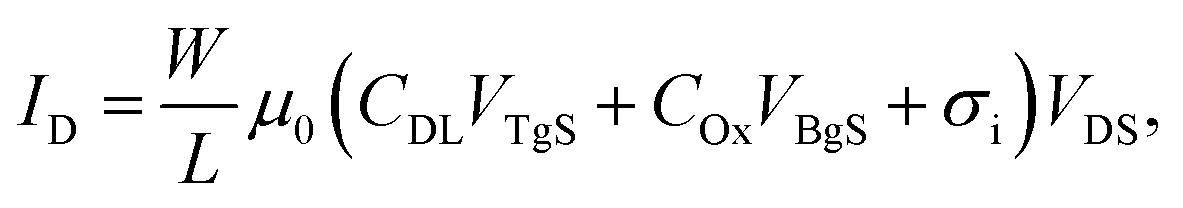 | (4) |
 | (5) |
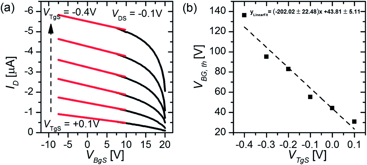 | ||
| Fig. 2 (a) Back-gate transfer curves (black lines) at VDS = −0.1 V recorded in DI-water with a Pt gate electrode and linear fits (red lines) at different electrolyte-gate voltages VTgS. (b) Threshold voltages extracted from the linear fit curves of the back-gate sweeps as a function of the electrolyte-gate potential and the corresponding linear fit curve. | ||
The threshold voltages were extrapolated from a linear fit (red lines, Fig. 2(a)) of the various transfer curves and plotted as a function of the applied top-gate voltage VTgS, as depicted in Fig. 2(b).
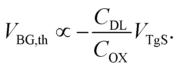
By using the slope k obtained from the linear fit of the VBG,thvs. VTgS dependence and taking into account the capacitance of the back-gate dielectric (thickness dOx = 65 nm, COx = 53.2 nF cm−2), the capacitance of the electrical double layer can be calculated according to eqn (5) (ref. 23).
We obtain a double layer capacitance of CDL (DI-H2O) = 10.8 ± 1.2 μF cm−2, which exceeds the literature values for P3HT in contact with deionized water (3–6 μF cm−2), as measured by impedance spectroscopy, by a factor of 2, but they are consistent with values obtained for metallic surfaces in contact with an electrolyte, ∼20 μF cm−2 for gold in contact with DI-water.12 Cramer et al.23 determined the double layer capacitance with a pentacene thin-film transistor with deionized water as the electrolyte. They obtained values of CDL (DI-H2O) = 7.8 μF cm−2,23 which is generally lower than the results obtained with the P3HT OTFT. One possible explanation could be that their semiconducting layer consists of less than six monolayers of pentacene and therefore has a much smoother surface than the P3HT film (see the AFM image in Fig. 1(c)) used in this work. In simplified terms, the huge surface roughness of the P3HT film results in an increased capacitance of the electrical double layer at the semiconductor–electrolyte interface since the geometrical size of the active area (4 mm × 4 mm) stays constant, whereas the effective contact area between the electrolyte and semiconductor increases with increasing surface roughness.
In general, the capacitance of the Debye–Helmholtz layer depends on the ionic strength of the electrolytic solution (see eqn (1) and (2)), therefore back-gate sweeps were not only recorded for different top-gate voltages but also in KCl solutions with varying ion concentrations. The obtained values for the double layer capacitance measured with a Pt wire as the gate electrode are shown in Fig. 3(a). The reduction of the capacitance to lower ionic strengths is in general agreement with theoretical models describing the Debye–Helmholtz layer.17–19 Again, the value obtained by Cramer et al.23 for a 100 mM solution of a monovalent salt (sodium chloride, NaCl) CDL (100 mM NaCl) = 14.6 μF cm−2 is lower than the EDL capacitance measured with the P3HT OTFT.
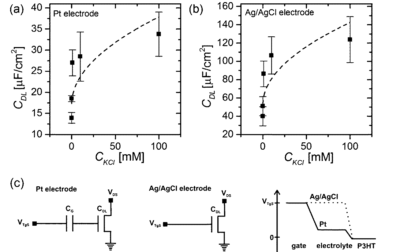 | ||
| Fig. 3 Capacitance of the electrical double layer CDL obtained (a) for a Pt-gated transistor and (b) with an Ag/AgCl electrode as the gate electrode as a function of the salt concentration. Panel (c) shows the equivalent circuits28 of a Pt gate electrode and an Ag/AgCl electrode immersed in the electrolytic solution. The right graph depicts the potential distribution between the gate electrode and the semiconducting channel for both electrode types.26 | ||
Additionally, the same measurements were performed with an Ag/AgCl electrode. The main difference between these two gate materials is that platinum can be seen as an ideally polarizable electrode when operated in an electrolytic solution with these relatively low voltages (|VTgS| < 1 V), which means that an electrical double layer forms at the interface between the gate-material and the electrolyte. However, due to the following reaction constantly taking place at the surface of the Ag/AgCl electrode, a steady-state current flows from the gate electrode to the electrolytic solution, and therefore no electrical double layer forms at the interface between the electrode and the electrolyte.26
| Ag + Cl− ↔ AgCl + e− | (6) |
This means that with a Pt wire immersed as the gate electrode in the electrolytic solution, the applied gate potential drops across two electrical double layers formed both at the electrode–electrolyte interface as well as at the electrolyte–semiconductor interface. On the contrary, for an Ag/AgCl electrode the whole potential has to drop across the electrical double layer formed at the electrolyte–semiconductor interface (see Fig. 3(c)).19,20,27,28
In a simple equivalent circuit, the Pt wire immersed in the electrolytic solution can be regarded as a capacitor CG (see Fig. 3(c)), which is connected in series with the capacitor CDL of the interface between the P3HT layer and the electrolytic solution, as shown in Fig. 3(a). Thus the effective gating capacitance of the OTFT operated with a Pt electrode is given by:28
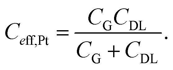 | (7) |
Therefore one would expect to measure a higher double layer capacitance CDL by operating the device with an Ag/AgCl electrode. Fig. 3(b) shows the double layer capacitance measured with an Ag/AgCl electrode as a function of the salt concentration present in the electrolyte.
For a KCl concentration of 100 mM we obtain a double layer capacitance of CDL (100 mM KCl, Ag/AgCl) = 123.77 ± 2.50 μF cm−2, which is about 4 times higher than with a Pt electrode, where CDL (100 mM KCl, Pt) = 33.78 ± 5.25 μF cm−2.
3.3 Simulation of electrolyte-gated field-effect transistors
For the simulation of the back-gated and electrolyte-gated OTFT devices we use a modified drift–diffusion model implemented into the commercial TCAD software Sentaurus. For a given device geometry, this software simulates charge transport by solving a set of equations, including the drift–diffusion equations, the continuity equations and the Poisson equation| Jn = −eμn∇ϕ + eDn∇n, | (8) |
| JP = −eμp∇ϕ − eDp∇p, | (9) |
| ∇·Jn = e(R − G), | (10) |
| ∇·Jp = −e(R − G), | (11) |
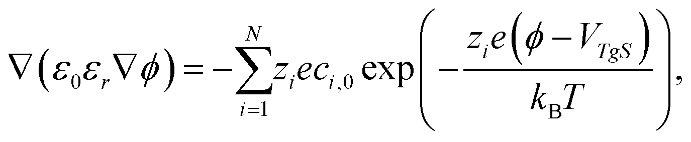
| ∇·(ε0εr∇ϕ) = e(n − p + N+D − N−A + pAt), | (12) |
 | (13) |
In a first approximation, the electrolyte will be taken into account as an insulating layer between the electrolyte-gate contact and the organic semiconductor region, according to the simple Helmholtz model (see Fig. 4(a)).31
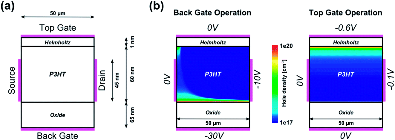 | ||
| Fig. 4 (a) Drift–diffusion simulation layout for the Helmholtz model. The electrolyte is taken into account by an insulating Helmholtz layer. (b) Comparison of back-gate operation and top-gate operation. The values of the boundary conditions are given at the respective contacts and are typical for the different operation modes. The hole density gives information as to where the conducting channel is formed. | ||
That way, the electrical double layer is modelled as a parallel plate capacitor (from here on referred to as the Helmholtz layer) accounting for a linear potential drop. The capacitance of this Helmholtz layer is taken from the experimentally extracted data to 28 μF cm−2 for an ion concentration of 10 mM, according to Section 3.2. As can be seen in Fig. 4(b), when operating with the top-gate contact the conductive channel is spatially shifted towards the electrolyte–semiconductor interface. This can be intuitively understood considering the electric field that is generated by the applied negative top-gate voltage and which attracts positive charge carriers towards this interface. The considerably low top-gate voltage is due to the large capacitive value of the Helmholtz layer compared to the oxide layer of the back-gate contact.
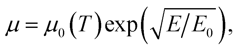
With this simulation setup, we simulate transfer and output curves in both back-gate and top-gate operation and compare them to experimental data to adjust the simulation parameters. The simulation of the back-gate operation has already been reported in the literature,32 and serves as a reference for the simulation parameters of the organic semiconductor material, such as density of states, unintentional doping, trap level distribution, low field mobility etc. These parameters are then used for the simulation of top-gate operation to give a conclusive self-consistent picture. All relevant simulation parameters are given in Table 1. The results of such a fitting procedure are shown in Fig. 5 for one selected device. The simulation of transfer curves in back-gate operation (Fig. 5(a)) shows good agreement with the experimental data in the accessible voltage range, and also the output curve is in the right order of magnitude. The low field mobility in that case is μ0 = 5 × 10⁻³ cm2 V−1 s−1, which is in good agreement with literature values.11,25 When simulating the top-gate operation (Fig. 5(b)), one can see that using this value for the low field mobility leads to a drastic underestimation of the drain current. There are two parameters in our model which affect the transconductance of the device, i.e. the slope of the linear transistor behaviour, the first being the capacitance of the Helmholtz layer and the second being the low field mobility. By changing the Helmholtz layer capacitance one would have to use unphysical values that are several orders of magnitude larger than what has been extracted experimentally, in order to fit the experimental data. Furthermore, this leads to large deviations from the experimental data in the sublinear regime as the curve becomes heavily kinked.
| Device T#01 | ||
|---|---|---|
| P3HT | LUMO | 3 eV |
| HOMO | 5 eV | |
| ε r | 3 | |
| DOS | 5 × 1020 cm−3 | |
| Doping concentration | N D | 1.2 × 1017 cm−3 |
| Poole–Frenkel mobility | μ 0 (back) | 5 × 10⁻³ cm2 V−1 s−1 |
| μ 0 (top) | 3 × 10⁻² cm2 V−1 s−1 | |
| E 0 | 3 × 10⁵ V cm−1 | |
| Shallow level trap | c 0,shall | 5 × 1012 cm−2 |
| E mid | 0.1 eV | |
| E sig | 0.2 eV | |
| Deep level trap | c 0,deep | 5 × 1012 cm−2 |
| E mid | 0.4 eV | |
| E sig | 0.3 eV | |
| Fixed charges | c fix (back) | −2.1 × 1012 cm−2 |
| c fix (top) | −2.1 × 1012 cm−2 | |
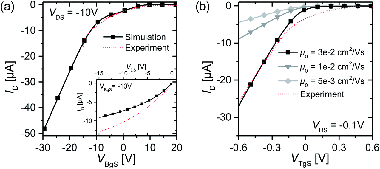 | ||
| Fig. 5 (a) Best fit of the back-gate operation transfer curve for one selected device. The inset shows an output curve at VBgS = −10 V. The mobility is μ0 = 5 × 10⁻³ cm2 V−1 s−1. (b) Fit of the top-gate operation transfer curve for device T#01 for different low field mobilities according to the Helmholtz model. The ion concentration in the electrolyte is 10 mM. All simulation parameters can be found in Table 1. | ||
On the other hand, when changing the mobility by about one order of magnitude, the transconductance of the experimental data can be matched correctly and also the deviations in the sublinear regime are not as pronounced. Such an elevated low field mobility hints at a physical change in the transport properties at the electrolyte–semiconductor interface. Cramer et al.33 stated that the reorientation of water dipoles at the electrolyte–semiconductor interface stabilizes positive charge carriers and leads to a polaronic trap state which remains highly mobile in the plane parallel to the interface. Their findings based on pentacene show a mobility elevated by about one order of magnitude.
They mention that the polaron binding energy depends only on water polarization and the spatial extension of the charge carriers in the organic semiconductor. Therefore, these findings can be generalized to other organic semiconductors and might give an explanation for the different mobilities for back-gate operation versus top-gate operation in our sensor devices. However, further investigations are needed in that direction.
In order to refine the simple approximation of the EDL as a parallel plate capacitor, one needs to account for a diffusive layer, the Gouy–Chapman layer, in the form of the Poisson–Boltzmann equation (PBe) according to the Stern model.34 The PBe reads
 | (14) |
4 Conclusion
In summary, we reported the measurement of the electrical double layer capacitance of a dual-gated P3HT OTFT by sweeping the back-gate potential with fixed electrolyte-gate potentials at the top-gate. We proved the dependency of the EDL capacitance on the ionic strength of the electrolyte and additionally we demonstrated the effect of a non-polarizable gate electrode in comparison to a polarizable electrode on the gating mechanism. With the experimentally obtained values for the capacitance of the Debye-Helmholtz layer at the semiconductor–electrolyte interface, we can model the electrolyte-gate transfer characteristics of the P3HT OTFT. Our study suggests that the mobility of the active material close to the semiconductor–electrolyte interface is larger than the bulk mobility.Acknowledgements
This work was partially supported by the International Graduate School for Science and Engineering (IGSSE), the Graduate School (TUM-GS) at the Technische Universität München, and the European Integrated Training Networks “Olimpia” and “OrgBio”.References
- L. Kergoat, B. Piro, M. Berggren, G. Horowitz and M.-C. Pham, Anal. Bioanal. Chem., 2012, 402, 1813–1826 CrossRef CAS PubMed
.
- P. Lin and F. Yan, Adv. Mater., 2012, 24, 34–51 CrossRef CAS PubMed
- J. T. Mabeck and G. G. Malliaras, Anal. Bioanal. Chem., 2006, 384, 343–353 CrossRef CAS PubMed
- A. M. Münzer, K. Melzer, M. Heimgreiter and G. Scarpa, Biochim. Biophys. Acta, 2013, 1830, 4353–4358 CrossRef PubMed
- C. Bartic, B. Palan, A. Campitelli and G. Borghs, Sens. Actuators, B, 2002, 83, 115–122 CrossRef CAS
- M. E. Roberts, S. C. B. Mannsfeld, N. Queraltó, C. Reese, J. Locklin, W. Knoll and Z. Bao, Proc. Natl. Acad. Sci. U. S. A., 2008, 105, 12134–12139 CrossRef CAS PubMed
- S. Casalini, F. Leonardi, T. Cramer and F. Biscarini, Org. Electron., 2013, 14, 156–163 CrossRef CAS PubMed
- M. D. Angione, S. Cotrone, M. Magliulo, A. Mallardi, D. Altamura, C. Giannini, N. Cioffi, L. Sabbatini, E. Fratini, P. Baglioni, G. Scamarcio, G. Palazzo and L. Torsi, Proc. Natl. Acad. Sci. U. S. A., 2012, 109, 6429–6434 CrossRef CAS PubMed
- M. Magliulo, A. Mallardi, M. Y. Mulla, S. Cotrone, B. R. Pistillo, P. Favia, I. Vikholm-Lundin, G. Palazzo and L. Torsi, Adv. Mater., 2013, 25, 2090–2094 CrossRef CAS PubMed
- G. Scarpa, A.-L. Idzko, S. Götz and S. Thalhammer, Macromol. Biosci., 2010, 10, 378–383 CrossRef CAS PubMed
- S. M. Goetz, C. M. Erlen, H. Grothe, B. Wolf, P. Lugli and G. Scarpa, Org. Electron., 2009, 10, 573–580 CrossRef CAS PubMed
- L. Kergoat, L. Herlogsson, D. Braga, B. Piro, M.-C. Pham, X. Crispin, M. Berggren and G. Horowitz, Adv. Mater., 2010, 22, 2565–2569 CrossRef CAS PubMed
- H. Klauk, Chem. Soc. Rev., 2010, 39, 2643–2666 RSC
- S. H. Kim, K. Hong, W. Xie, K. H. Lee, S. Zhang, T. P. Lodge and C. D. Frisbie, Adv. Mater., 2013, 25, 1822–1846 CrossRef CAS PubMed
- S. H. Kim, K. Hong, W. Xie, K. H. Lee, S. Zhang, T. P. Lodge and C. D. Frisbie, Adv. Mater., 2013, 25, 1822–1846 CrossRef CAS PubMed
- T. Cramer, A. Campana, F. Leonardi, S. Casalini, A. Kyndiah, M. Murgia and F. Biscarini, J. Mater. Chem. B, 2013, 1, 3728–3741 RSC
- P. J. Boddy, J. Electroanal. Chem., 1965, 199–244 CAS
- D. C. Grahame, Chem. Rev., 1947, 41, 441–501 CrossRef CAS
-
A. J. Bard and L. R. Faulkner, Electrochemical Methods-Fundamentals and Applications, Wiley, New York, 2001 Search PubMed
- M. Waleed Shinwari, M. Jamal Deen and D. Landheer, Microelectron. Reliab., 2007, 47, 2025–2057 CrossRef PubMed
- M. E. Roberts, S. C. B. Mannsfeld, R. M. Stoltenberg and Z. Bao, Org. Electron., 2009, 10, 377–383 CrossRef CAS PubMed
- C. J. Bettinger and Z. Bao, Adv. Mater., 2010, 22, 651–655 CrossRef CAS PubMed
- T. Cramer, A. Kyndiah, M. Murgia, F. Leonardi, S. Casalini and F. Biscarini, Appl. Phys. Lett., 2012, 100, 143302 CrossRef PubMed
- M.-J. Spijkman, K. Myny, E. C. P. Smits, P. Heremans, P. W. M. Blom and D. M. de Leeuw, Adv. Mater., 2011, 23, 3231–3242 CrossRef CAS PubMed
- A. Salleo, T. W. Chen, A. R. Völkel and R. A. Street, Phys. Rev. B: Condens. Matter Mater. Phys., 2004, 70, 1–10 Search PubMed
- G. Tarabella, C. Santato, S. Y. Yang, S. Iannotta, G. G. Malliaras and F. Cicoira, Appl. Phys. Lett., 2010, 97, 123304 CrossRef PubMed
- G. Tarabella, C. Santato, S. Y. Yang, S. Iannotta, G. G. Malliaras and F. Cicoira, Appl. Phys. Lett., 2010, 97, 123304 CrossRef PubMed
- P. Lin, F. Yan and H. L. W. Chan, ACS Appl. Mater. Interfaces, 2010, 2, 1637–1641 CAS
- A. Bolognesi, A. Di Carlo and P. Lugli, Appl. Phys. Lett., 2002, 81, 4646 CrossRef CAS PubMed
- A. Bolognesi, M. Berliocchi, M. Manenti, A. Di Carlo, P. Lugli, K. Lmimouni and C. Dufour, IEEE Trans. Electron Devices, 2004, 51, 1997–2003 CrossRef CAS
- H. Helmholtz, Ann. Phys. Chem., 1853, 165, 211–233 CrossRef
- A. Khaliq, F. L. Xue and K. Varahramyan, Microelectron. Eng., 2009, 86, 2312–2315 CrossRef CAS PubMed
- T. Cramer, T. Steinbrecher, T. Koslowski, D. A. Case, F. Biscarini and F. Zerbetto, Phys. Rev. B: Condens. Matter Mater. Phys., 2009, 79, 155316 CrossRef
- O. Stern, Z. Elektrochem. Angew. Phys. Chem., 1924, 30, 508–516 CAS
| This journal is © The Royal Society of Chemistry 2014 |