 Open Access Article
 This Open Access Article is licensed under a
 Creative Commons Attribution 3.0 Unported Licence
Organic semiconductor distributed feedback laser pixels for lab-on-a-chip applications fabricated by laser-assisted replication
Xin
Liu
ab,
Stephan
Prinz†
a,
Heino
Besser
cd,
Wilhelm
Pfleging
cd,
Markus
Wissmann
bd,
Christoph
Vannahme‡
ba,
Markus
Guttmann
bd,
Timo
Mappes§
b,
Sebastian
Koeber
be,
Christian
Koos
be and
Uli
Lemmer
*ab
aLight Technology Institute (LTI), Karlsruhe Institute of Technology, 76131 Karlsruhe, Germany. E-mail: uli.lemmer@kit.edu
bInstitute of Microstructure Technology (IMT), Karlsruhe Institute of Technology, 76344 Eggenstein-Leopoldshafen, Germany
cInstitute for Applied Materials - Applied Materials Physics (IAM-AWP), Karlsruhe Institute of Technology, 76344 Eggenstein-Leopoldshafen, Germany
dKarlsruhe Nano Micro Facility, Hermann-von-Helmholtz-Platz 1, 76344 Eggenstein-Leopoldshafen, Germany
eInstitute of Photonics and Quantum Electronics (IPQ), Karlsruhe Institute of Technology, 76131 Karlsruhe, Germany
First published on 7th August 2014
Abstract
The integration of organic semiconductor distributed feedback (DFB) laser sources into all-polymer chips is promising for biomedical or chemical analysis. However, the fabrication of DFB corrugations is often expensive and time-consuming. Here, we apply the method of laser-assisted replication using a near-infrared diode laser beam to efficiently fabricate inexpensive poly(methyl methacrylate) (PMMA) chips with spatially localized organic DFB laser pixels. This time-saving fabrication process enables a pre-defined positioning of nanoscale corrugations on the chip and a simultaneous generation of nanoscale gratings for organic edge-emitting laser pixels next to microscale waveguide structures. A single chip of size 30 mm × 30 mm can be processed within 5 min. Laser-assisted replication allows for the subsequent addition of further nanostructures without a negative impact on the existing photonic components. The minimum replication area can be defined as being as small as the diode laser beam focus spot size. To complete the fabrication process, we encapsulate the chip in PMMA using laser transmission welding.
1 Introduction
Organic semiconductor distributed feedback (DFB) lasers are of particular interest as tunable laser emitters covering the whole visible spectral range.1–5 Enabled by the efficient conversion in their active material, low threshold organic semiconductor lasers allow for free space and integrated excitation sources in spectroscopic investigations.6–9 In particular, the integration of miniaturized laser light sources in all-polymer lab-on-a-chip (LOC) platforms is promising for point-of-care systems.10–14 In order to realize laser pixels, technologies for local definition of the active material, and for the laterally controlled fabrication of DFB structures, have to be developed.In terms of the gain materials, small molecules such as tris(8-hydroxyquinoline) aluminum (Alq3) doped with the laser dye 4-(dicyanomethylene)-2-methyl-6-(p-dimethylaminostyryl)-4H-pyran (DCM) compete with conjugated polymers. The former class of materials can be evaporated locally using shadow masking, and can thus be combined with pre-defined grating structures. On the other hand, conjugated polymers can be processed by inexpensive solution-based techniques such as spin coating, dip-coating and doctor blading. These methods, however, result in an organic semiconductor layer covering the whole substrate. Lateral control can be achieved using printing techniques. A particularly interesting approach is the use of ink-jet printing. Ink-jet printing has already been successfully applied to the fabrication of various organic electronic devices, such as organic transistors,15,16 organic solar cells17,18 and organic light-emitting diodes.19,20 We have recently successfully fabricated organic semiconductor distributed feedback laser pixels by ink-jet printing the active layer from a conjugated polymer solution. Utilizing an optimized mixture of high-boiling and low-boiling solvents for dissolving the polymer, the ink-jet-printed film profile is optimized, thus creating uniformly emitting organic lasers. Such devices show lasing thresholds as low as 76 nJ per pulse and a spectrally homogeneous laser emission over large areas.21
The laterally controlled fabrication of DFB gratings for organic semiconductor lasers has only been addressed so far by using nanograting transfer to transfer the gratings onto a homogeneous gain material layer,22 and a rather complex approach using direct electron beam lithography (EBL) on conjugated polymers.23 On the other hand, various substrate scale techniques such as laser interference lithography (LIL)24 and nanoimprint lithography (NIL)25 are available to achieve the low-cost fabrication of high-quality DFB corrugation nanostructures on an LOC platform. Among them, NIL promises the mass-production of extremely fine structures with feature sizes down to 10 nm.26 The resolution of NIL can be further improved by the fabrication of a rigid mold with sub-10 nm features.25 Nowadays, two main subjects of NIL are frequently used in the fabrication of DFB corrugations for organic semiconductor laser applications: thermal nanoimprint lithography (TNIL, also known as hot embossing) and UV-assisted nanoimprint lithography (UV-NIL).27–30 UV-NIL is an option to fabricate localized DFB corrugations without negative effects on the existing structures, but it is mandatory to use special photoactive materials in the process. This limitation results in a narrow application field in the fabrication of LOC systems. TNIL is advantageous for parallel replication of all structures from a master stamp onto a common polymer substrate. Nevertheless, it has three major drawbacks. First is the difficulty in the fabrication of pre-defined partial structures from a rigid master stamp with structures for different purposes. Secondly, the large-area heating can be detrimental for existing LOC passive photonic elements and microfluidic channels. The third issue is the long heating and cooling time.
These limitations of TNIL can be overcome using a near-infrared high-power diode laser beam.31,32 In this work, we demonstrate a novel laser-assisted replication to fabricate localized surface-emitting (2nd order) and edge-emitting (1st order) organic distributed DFB laser pixels on a poly(methyl methacrylate) (PMMA) substrate. Our technique allows for fast replication with standard TNIL materials due to the localized heating. Not only is the process time reduced, the localized heating also provides the unique benefit to replicate only parts of the existing structures on a master stamp. Additionally, since only the defined areas are to be heated, it allows for subsequent additive fabrication of DFB corrugations while all the other areas are retained. The minimum localized replication area and the influence of the process parameters on corrugation quality are investigated. A functional LOC is finished after encapsulation via laser transmission welding, protecting the device from air and water.33–35
2 Fabrication process
In laser-assisted replication, a rigid mold, e.g., a silicon master stamp, is pressed under a polymer substrate, and the contact area is subsequently heated up by a near-infrared laser beam from above, as shown in Fig. 1(a). Due to heat conduction, the temperature of the polymer material, which is in direct contact with the master stamp, increases. When the temperature exceeds the polymer glass transition temperature, the nanostructures on the rigid mold are replicated into the polymer substrate. After cooling down, the polymer substrate is detached from the rigid mold, while the nanostructures are preserved.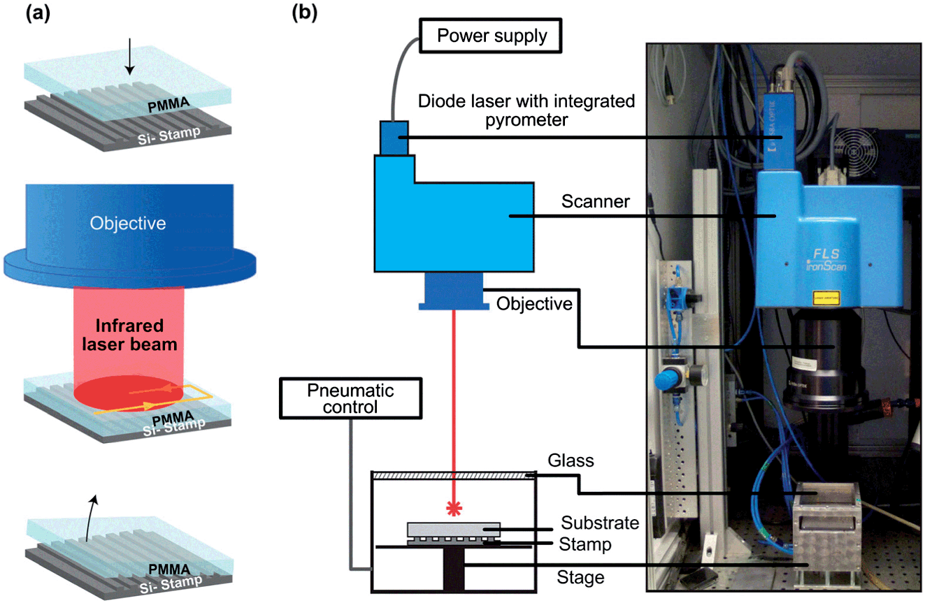 | ||
| Fig. 1 (a) Scheme of the laser-assisted replication process: positioning of the PMMA substrate on a silicon master stamp (top), execution of the replication (middle), and detachment of the sample (bottom). (b) Schematic illustration (left) and photograph (right) of the applied laser system. | ||
To perform the experiments, a high-power diode laser system (Fisba Optik, FLS Iron High Power Diode) with an emission wavelength of 940 nm and a maximal power of 50 W is used. As shown in Fig. 1(b), the diode laser and a pyrometer, which provides in situ monitoring of the temperature at the laser focus plane, are integrated within the laser scanner unit. The PMMA substrate and the silicon master stamp are fixed in a pneumatic stage, applying a constant pressure. There are two basic operation modes of the system: constant laser power or constant heating temperature. In our case, the temperature regulation is chosen in order to achieve a homogeneous temperature distribution at the contact surface. Utilizing an F-Theta objective lens (Fisba Optik) with a focal length of 163 mm, the size of the elliptical laser focus spot on the work plane is 0.55 mm × 0.7 mm. Attributed to the applied scanner system, the maximum laser processing area can reach 100 mm × 100 mm.
Before replication, a silicon master stamp was fabricated. Via electron beam lithography and reactive ion etching (RIE), the DFB corrugations with grating periods ranging from 195 nm to 450 nm, a height of ∼120 nm and a duty cycle of 75% were generated. Via aligned UV-lithography and subsequent RIE on the same wafer, basins for the DFB lasers with a height of 1.2 μm were completed. A thin anti-adhesion layer was then deposited on the wafer to facilitate the polymer substrate detachment.13
For the replication process, a 2 mm-thick PMMA substrate (Evonik, Plexiglas® XT) with a size of 30 mm × 30 mm was positioned on selected corrugations of the silicon master stamp. The following process parameters resulted in the highest-quality replication: a heating temperature of T = 180 °C, a laser scan velocity of v = 40 mm s−1, a clamping pressure of p = 0.1 MPa and a hatch distance (offset between two neighboring laser tracks) of Δx = 300 μm. To achieve a homogeneous replication, each substrate was treated twice by the laser beam: firstly perpendicular to the grating orientation, as shown in Fig. 1(a), and secondly parallel to the grating orientation. The replication process took about 5 min for the replication of an area of 40 mm × 40 mm. After replication, the clamping pressure was released. The PMMA substrate was cooled down with a nitrogen spray gun and separated from the silicon master stamp. Fig. 2(a) and (b) show a microscope image and a scanning electron microscope image on PMMA of a grating with a period of Λ = 400 nm. The grating structures fabricated via laser-assisted replication show a high fidelity over the whole molding area. The replicated quality was similar to thermal nanoimprint lithography, as shown in Fig. 2(c). However, the laser-assisted replication process took a much shorter time compared to the 45 min-long TNIL process. Alq3 doped with the laser dye DCM has been chosen as the active material. It forms a very efficient Förster energy transfer system and exhibits an excellent long-term stability. Evaporating 250 nm Alq3 doped with 2.8 wt% DCM onto the defined grating fields finally yielded the organic DFB laser pixels. The used stencil shadow mask was fabricated by UV-lithography and nickel electroplating.14
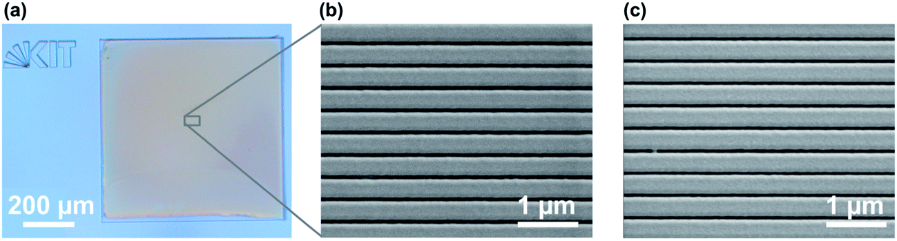 | ||
| Fig. 2 (a) Microscope image of a one-dimensional PMMA DFB grating with a period of Λ = 400 nm fabricated by laser-assisted replication. (b) Scanning electron microscope image of the grating structures fabricated by laser-assisted replication. For comparison, (c) shows a scanning electron microscope image of the Λ = 400 nm grating structures fabricated by thermal nanoimprint lithography (equipment built by Institute of Microstructure Technology-KIT) using the same silicon master stamp as for (b). A temperature of 180 °C and a pressure of 1.85 MPa were applied for 15 min. The total TNIL process lasted for ∼45 min. | ||
3 DFB laser characterization
For optical characterization, the fabricated surface-emitting organic DFB lasers were excited by a diode-pumped, actively Q-switched frequency tripled neodymium:yttrium orthovanadate (Nd:YVO4) laser (Advanced Optical Technology Ltd., AOT-YVO-20QSP) with a wavelength of 355 nm. The pump pulse had a duration of approximately 1 ns at a repetition rate of 1 kHz. The pump pulse energy was adjusted with a variable neutral density filter and measured with a calibrated gallium arsenide phosphide photodiode connected to an oscilloscope (Tektronix, TDS2024C). The sample was kept in a vacuum chamber (<5 × 10⁻³ Pa) to protect the active material from photooxidation. The chamber can be shifted in the plane perpendicular to the excitation beam using an automated precision stage. This allows for a spectrally and spatially resolved characterization of the samples. A focusing lens was used to adjust the excitation spot size. The emission from the sample was collected using the focusing lens for the pump beam, then directed through a dichroic mirror and coupled into a multimode optical fiber. Further on, the laser spectra were analyzed using a spectrograph (Acton Research Corporation, SpectraPro 300i, variable grating) connected to an intensified charge-coupled device camera (Princeton Research, PiMax 512). The pump spot showed a slightly elliptical shape with a size of 30 μm × 40 μm on the sample.Fig. 3(a) shows the color-encoded spatially resolved lasing wavelength from a PMMA chip containing 9 laser pixels with individual lateral dimensions of 500 μm × 500 μm and an interspacing of 500 μm. The grating period of the DFB corrugations varies from 370 nm to 450 nm in steps of 10 nm from the outermost left pixel to the outermost right pixel. The chip was probed with a resolution of 100 μm. The laser emission wavelength did not show any deviation on the area of a single laser pixel within the spectral resolution of the setup (approximately 0.5 nm). This indicates a very uniform replication of the nanogratings in PMMA. The corresponding laser emission spectra and the laser threshold values for the TE0-modes are shown in Fig. 3(b) and (c). The blue-shifted TM0-mode laser peaks identified with a polariser can be detected at λ = 630.4 nm and λ = 643.6 nm. These peaks originate from the lasers with grating periods of Λ = 400 nm and Λ = 410 nm. The higher laser threshold from the laser pixel with a grating period of 450 nm is attributed to the lower gain coefficient at the emission wavelength of 712.5 nm.
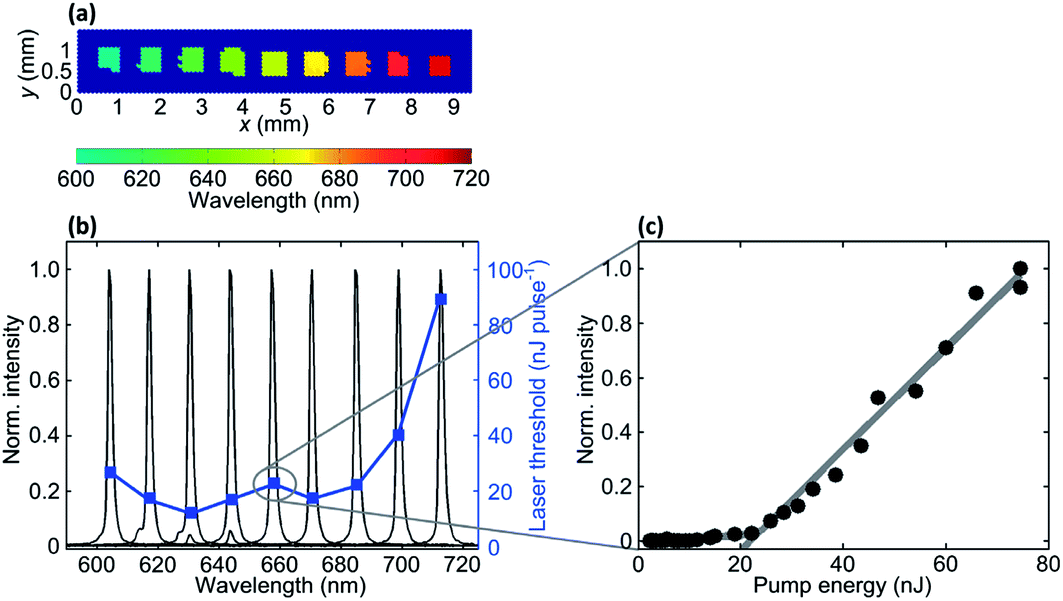 | ||
| Fig. 3 (a) Color-encoded spatially resolved laser wavelengths of the fabricated organic DFB laser pixels with grating periods from 370 nm (left) to 450 nm (right) in steps of 10 nm. (b) Laser spectra and TE0-mode laser threshold corresponding to the grating distribution. For some gratings the onset of the TM0-mode can also be seen as very small peaks. (c) Input–output characteristics of a laser pixel with a grating period of Λ = 410 nm and a laser emission at λ = 657.5 nm. | ||
For being suitable for LOC spectroscopic applications, the organic semiconductor lasers are usually based on first-order DFB gratings for the emission of light in the chip plane only. By introducing a waveguide onto the chip, the first-order organic laser emission can be efficiently coupled and guided to the analyte sites. PMMA chips with deep ultraviolet (DUV)-induced waveguides have been fabricated previously.11,13 In this work, we fabricated the active grating and waveguides altogether via laser-assisted replication and evaporated Alq3:DCM on both of them to build a coupled edge-emitting organic laser on chip. This novel configuration allows for a one-step fabrication of the laser and waveguide without mix-and-match pattern-related defects.36 Besides, the direct connection between the laser and waveguide made from the same active material will facilitate an optimum coupling efficiency.
Different gratings with lateral dimensions of 500 μm, interconnected by 300 μm-wide waveguide structures perpendicular to the grating orientation, were simultaneously fabricated in 1.2 μm-deep basins on the PMMA chip. The grating periods for the first-order organic DFB laser were chosen to be Λ = 195 nm, Λ = 200 nm, and Λ = 205 nm, as marked in Fig. 4(a). A 250 nm-thick layer of Alq3:DCM was evaporated on the defined grating and waveguide, thus allowing for an optimum light coupling.
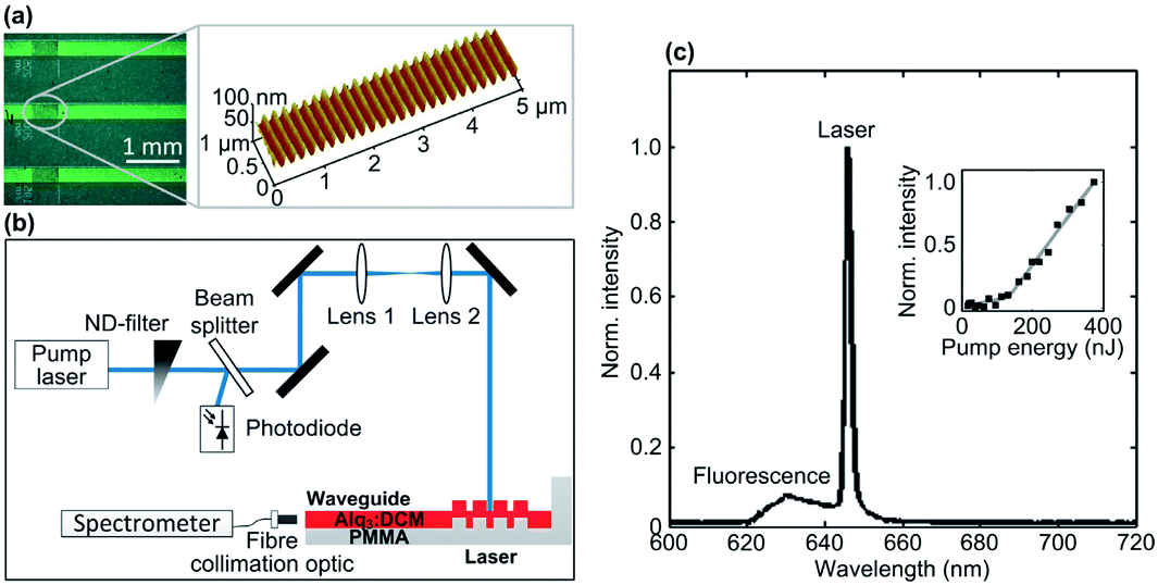 | ||
| Fig. 4 (a) Microscope image of a coupled organic DFB edge-emitting laser (left) and an atomic force micrograph of the nanograting with a period of Λ = 200 nm (right). (b) Schematic illustration of the optical setup to detect the edge emission from the integrated organic DFB laser. (c) Laser spectrum and input–output curve (inset) taken from the chip facet of a grating of Λ = 200 nm using a multimode optical fiber coupled to a spectrometer. | ||
The experimental setup for the chip characterization is schematically depicted in Fig. 4(b). The pump laser and the detection system were the same as used for the characterization of the surface-emitting organic lasers, but we changed the detection plane according to the chip orientation. The excitation spot diameter on the sample surface was ∼100 μm. In order to limit laser degradation in the ambient atmosphere, we set the excitation repetition rate as low as 100 Hz. Fig. 4(c) shows the laser spectrum of a DFB laser with a grating period of Λ = 200 nm. The laser emission at λ = 645.5 nm was detected at the chip facet using a multimode optical fiber (Ocean Optics, P400-3-UV-VIS). A stronger background due to the Alq3:DCM fluorescence than in the case of the surface-emitting lasers is observed. This can be explained by the fact that the fluorescence is coupled into the waveguide with comparable efficiency to the laser radiation. In the case of surface-emitting lasers, the fluorescence is almost not detected as it is emitted in all directions. The corresponding laser threshold was measured to be 145 nJ per pulse. This higher threshold can be explained by the laser being pumped at a larger excitation spot size than for the surface-emitting lasers.
4 Size dependence of laser-assisted replication
The minimum replication area size is determined by the applied laser beam diameter, the used processing time, and the laser-induced heating temperature in the contact zone of the master stamp and polymer. To investigate the spatial resolution limits of the replication process, we fabricated test structures with a tool comprising spatially defined DFB grating areas via laser-assisted replication using different heating periods. Fig. 5(a) shows a microscope image of the beginning trail of the replicated structure, which was obtained by laser-induced heating of a single line with a scanning speed of 40 mm s−1, corresponding to a ∼17.5 ms-long local heating. The red line indicates a fit to the right end of the replicated structures. The rim is in good accordance with the elliptical laser focus spot size of 0.55 mm × 0.7 mm.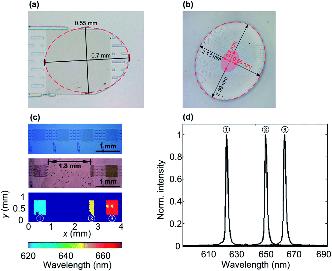 | ||
| Fig. 5 Microscope images of (a) the beginning of the replication trail obtained by heating a single line with a laser scanning velocity of 40 mm s−1, and (b) the replicated spot after 2 s-long punctuated heating in comparison with the laser focus spot (red). (c) Photograph of the complete set of spatially defined laser gratings (from left to right: Λ = 390 nm, Λ = 400 nm, Λ = 410 nm and Λ = 420 nm) on a silicon master stamp (top). The actual laser grating areas are visible as homogeneous darker grey areas which are separated by auxiliary structures in between. Photographs of the PMMA laser pixels partially replicated on a PMMA chip (middle) and spatially resolved laser wavelengths of the fabricated organic DFB laser pixels (bottom) are also shown. (d) Laser spectra corresponding to the grating areas ➀, ➁ and ➂ in (c). | ||
In comparison, applying 2 s-long punctuated heating resulted in an expansion of the heat-affected zone on the silicon stamp and a consequently enlarged replication area. As shown in Fig. 5(b), an extension was measured as ∼3.8 times that of the laser focus spot size.
We verified the versatility of the localized replication by the fabrication of pre-selected laser pixels. Fig. 5(c) shows a partial replication from the silicon master stamp with gratings in periods of Λ = 390 nm, Λ = 400 nm, Λ = 410 nm and Λ = 420 nm. Each pixel has a dimension of 500 μm × 500 μm with an interspacing of 500 μm. A 2 mm-broad space was excluded from the laser writing path from left to right on the chip. As a result, we observed an unstructured area with a width of 1.8 mm between the replicated structures. The slight difference between the size of the unstructured area and the non-irradiated area is attributed to the heat conduction in the silicon master stamp. The spatially resolved lasing wavelength distribution revealed one completely omitted and one only partially available laser pixel. The latter had a clearly defined border. The corresponding laser pixel spectra are shown in Fig. 5(d).
As previously mentioned, a great advantage of the localized replication is the subsequent fabrication of nanostructures with already existing photonic, fluidic or electronic components, which remain unaffected during the fabrication process. We demonstrated this by replicating the same structures twice on a single 2 mm-thick PMMA substrate and performing two successive replication processes at a distance of 10 mm. Each replicated area was defined to be 5 × 20 mm2 without overlapping each other, as shown in Fig. 6(a). Fig. 6(b) shows a photograph of the finished laser pixels on the PMMA chip, which can be clearly identified by the interference effect. A 250 nm-thick Alq3:DCM layer was evaporated on top of the chip to check the laser behavior and determine the replication quality. All the laser pixels showed homogeneous laser emissions throughout the whole pixel area with corresponding wavelengths according to their DFB grating periods. Laser pixels featuring the same grating period revealed comparable characteristics, e.g., the laser thresholds of the laser pixels with a grating period of Λ = 420 nm were measured to be 17.3 nJ per pulse and 14.8 nJ per pulse, both emitting at the same laser peak wavelength of λ = 670 nm. The existing grating structures were not influenced by the subsequent replication process. This can be widely useful for LOC and other integrated optics applications. The inexpensive fabrication of identical nanostructures without repetitive construction on a master stamp is shown to be possible.
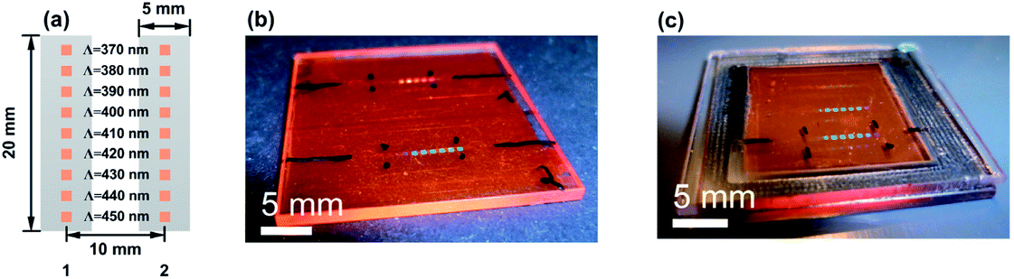 | ||
| Fig. 6 (a) Scheme of the first and second laser-assisted replication areas of size 5 mm × 20 mm. (b) Photograph of the subsequently fabricated grating structures 1 and 2. (c) Finished chip after encapsulation with a PMMA lid via laser transmission welding. The chip edge appears silver due to the absorption layer of carbon. | ||
5 Encapsulation via laser transmission welding
During operation, organic semiconductors suffer from photoluminescence degradation when exposed to air or water. Therefore, encapsulation is necessary to sustain the long lifetime of the device. Previously, LOCs containing organic semiconductor lasers have been encapsulated in a polymer using thermal bonding,12,13 which is usually time-consuming and therefore only suitable for parallel processing with large numbers of LOC chips. In addition, the high temperature used for bonding leads to bleaching of the organic dyes. Here, we demonstrate the encapsulation of our fabricated organic laser chip via laser transmission welding.33 For this purpose, the same setup as for laser-assisted replication was used, as shown in Fig. 1. A 2 mm-thick PMMA substrate was prepared as a lid and placed on top of the previously fabricated chip with laser-pixel basins. Since PMMA is transparent to near-infrared radiation, an additional absorption layer of carbon with a thickness of 5–10 nm was deposited under the polymer chip, where the welding process was to be performed (chip edge). Applying the diode laser beam at a wavelength of λ = 940 nm and a maximum power of 50 W on the chip edge with a 5 mm-wide margin, the absorption layer converted the laser radiation into heat, which melted the two PMMA substrates along the contact area and bound them together (heating temperature T = 140 °C, laser scan velocity v = 40 mm s−1; clamping pressure p = 0.4 MPa, hatch distance Δx = 300 μm). A photograph of the encapsulated organic laser chip is shown in Fig. 6(c). As expected, the encapsulation process was found not to affect the emission properties of the laser pixels. Laser transmission welding is thus not only a practical tool for chip bonding direct after laser-assisted replication, but also can be a substitute for thermal bonding after the thermal nanoimprint lithography process.6 Conclusion
In summary, we have successfully applied laser-assisted replication in the fabrication of spatially localized organic semiconductor DFB laser pixels on PMMA chips. We accomplished nine surface-emitting laser pixels based on nanogratings with different periods in lateral dimensions of 500 μm × 500 μm on a PMMA substrate. We also realized the simultaneous fabrication of nanoscale DFB corrugations and neighboring microscale waveguide basins. After evaporation of the same active material, coupled edge-emitting organic lasers were achieved with a combination of the functional waveguides. The minimum fabrication area size was investigated by comparing the replication spot with the laser beam focus size, and the versatility of the spatially localized replication was verified by the fabrication of pre-selected laser pixels. We also proved that using this fabrication method, further nanostructures could be added into the chip platform without a negative influence on the neighboring photonic components. Consequently, laser-assisted replication is an ideal tool for the fast and flexible fabrication of micro- and nanostructures with high quality, and is especially suited for the rapid prototyping of LOC platforms. Finally, we completed the chip fabrication by encapsulation of the polymeric chip using laser transmission welding. This progress in the additive fabrication of gratings can ideally be combined with our recent progress in ink-jet printing the active gain medium of organic semiconductors. By using different laser pixels, this approach allows for the realization of digitally manufactured versatile coherent light sources integrated in photonic microsystems and LOC devices.Acknowledgements
The authors thank A. Bacher, P.-J. Jakobs and A. Muslija for the silicon master stamp fabrication and P. Abaffy for taking the scanning electron microscope images. This work was supported by the Deutsche Forschungsgemeinschaft and the State of Baden-Württemberg through the DFG-Center for Functional Nanostructures (CFN). The work of X. L. is supported by Carl Zeiss Stiftung and Karlsruhe School of Optics & Photonics (KSOP). We acknowledge support by Deutsche Forschungsgemeinschaft and the Open Access Publishing Fund of Karlsruhe Institute of Technology. Finally, the support for laser processing by the Karlsruhe Nano Micro Facility (KNMF, http://www.knmf.kit.edu), a Helmholtz research infrastructure at the Karlsruhe Institute of Technology is gratefully acknowledged.References
- N. Tessler, G. J. Denton and R. H. Friend, Lasing from conjugated-polymer microcavities, Nature, 1996, 382, 695–697 CrossRef CAS.
- F. Hide, M. A. Diaz-Garcia, B. J. Schwartz, M. R. Andersson, Q. B. Pei and A. J. Heeger, Semiconducting polymers: a new class of solid-state laser materials, Science, 1996, 273, 1833–1836 CrossRef CAS.
- S. V. Frolov, M. Ozaki, W. Gellermann, Z. V. Vardeny and K. Yoshino, Mirrorless lasing in conducting polymer poly(2,5-dioctyloxy-p-phenylenevinylene) films, Jpn. J. Appl. Phys., 1996, 35, L1371–L1373 CAS.
- I. D. W. Samuel and G. A. Turnbull, Organic semiconductor lasers, Chem. Rev., 2007, 107, 1272–1295 CrossRef CAS PubMed.
- S. Klinkhammer, X. Liu, K. Huska, Y. Shen, S. Vanderheiden, S. Valouch, C. Vannahme, S. Bräse, T. Mappes and U. Lemmer, Continuously tunable solution-processed organic semiconductor DFB lasers pumped by laser diode, Opt. Express, 2012, 20, 6357–6364 CrossRef CAS PubMed.
- Y. Oki, S. Miyamoto, M. Maeda and N. J. Vasa, Multiwavelength distributed feedback dye laser array and its application to spectroscopy, Opt. Lett., 2002, 27, 1220–1222 CrossRef PubMed.
- T. Woggon, S. Klinkhammer and U. Lemmer, Compact spectroscopy system based on tunable organic semiconductor lasers, Appl. Phys. B, 2010, 99, 47–51 CrossRef CAS.
- S. Klinkhammer, T. Woggon, C. Vannahme, T. Mappes and U. Lemmer, Optical spectroscopy with organic semiconductor lasers, Proc. SPIE, 2010, 7722, 77221I CrossRef.
- X. Liu, P. Stefanou, B. Wang, T. Woggon, T. Mappes and U. Lemmer, Organic semiconductor distributed feedback (DFB) laser as excitation source in Raman spectroscopy, Opt. Express, 2013, 21, 28941–28947 CrossRef PubMed.
- T. Mappes, C. Vannahme, M. Schelb, U. Lemmer and J. Mohr, Design for optimized coupling of organic semiconductor laser light into polymer waveguides for highly integrated bio-photonic sensors, Microelectron. Eng., 2009, 86, 1499–1501 CrossRef CAS.
- C. Vannahme, S. Klinkhammer, A. Kolew, P.-J. Jakobs, M. Guttmann, S. Dehm, U. Lemmer and T. Mappes, Integration of organic semiconductor lasers and single-mode passive waveguides into a PMMA substrate, Microelectron. Eng., 2010, 87, 693–695 CrossRef CAS.
- C. Vannahme, M. B. Christiansen, T. Mappes and A. Kristensen, Optofluidic dye laser in a foil, Opt. Express, 2010, 18, 9280–9285 CrossRef CAS PubMed.
- C. Vannahme, S. Klinkhammer, M. B. Christiansen, A. Kolew, A. Kristensen, U. Lemmer and T. Mappes, All-polymer organic semiconductor laser chips: parallel fabrication and encapsulation, Opt. Express, 2010, 18, 24881–24887 CrossRef CAS PubMed.
- C. Vannahme, S. Klinkhammer, U. Lemmer and T. Mappes, Plastic lab-on-a-chip for fluorescence excitation with integrated organic semiconductor lasers, Opt. Express, 2011, 19, 8179–8186 CrossRef CAS PubMed.
- H. Sirringhaus, T. Kawase, R. H. Friend, T. Shimoda, M. Inbasekaran, W. Wu and E. P. Woo, High-resolution inkjet printing of all-polymer transistor circuits, Science, 2000, 290, 2123–2126 CrossRef CAS PubMed.
- H. E. Katz, Recent advances in semiconductor performance and printing processes for organic transistor-based electronics, Chem. Mater., 2004, 16, 4748–4756 CrossRef CAS.
- C. N. Hoth, P. Schilinsky, S. A. Choulis and C. J. Brabec, Printing highly efficient organic solar cells, Nano Lett., 2008, 8, 2806–2813 CrossRef CAS PubMed.
- T. Aernouts, T. Aleksandrov, C. Girotto, J. Genoe and J. Poortmans, Polymer based organic solar cells using ink-jet printed active layers, Appl. Phys. Lett., 2008, 92, 033306 CrossRef.
- T. R. Hebner, C. C. Wu, D. Marcy, M. H. Lu and J. C. Sturm, Ink-jet printing of doped polymers for organic light emitting devices, Appl. Phys. Lett., 1998, 72, 519–521 CrossRef CAS.
- J. Bharathan and Y. Yang, Polymer electroluminescent devices processed by inkjet printing: I. Polymer light-emitting logo, Appl. Phys. Lett., 1998, 72, 2660–2662 CrossRef CAS.
- X. Liu, S. Klinkhammer, K. Sudau, N. Mechau, C. Vannahme, J. Kaschke, T. Mappes, M. Wegener and U. Lemmer, Ink-jet-printed organic semiconductor distributed feedback laser, Appl. Phys. Express, 2012, 5, 072101 CrossRef.
- X. Liu, S. Klinkhammer, Z. Wang, T. Wienhold, C. Vannahme, P.-J. Jakobs, A. Bacher, A. Muslija, T. Mappes and U. Lemmer, Pump spot size dependent lasing threshold in organic semiconductor DFB lasers fabricated via nanograting transfer, Opt. Express, 2013, 21, 27697–27706 CrossRef PubMed.
- R. Stabile, A. Camposeo and L. Persano, Organic-based distributed feedback lasers by direct electron-beam lithography on conjugated polymers, Appl. Phys. Lett., 2007, 91, 101110 CrossRef.
- M. Stroisch, T. Woggon, U. Lemmer, G. Bastian, G. Violakis and S. Pissadakis, Organic semiconductor distributed feedback laser fabricated by direct laser interference ablation, Opt. Express, 2007, 15, 3968–3973 CrossRef CAS PubMed.
- N. R. Hendricks and K. R. Carter, Nanoimprint lithography of polymers, in Polymer Science: A Comprehensive Reference, Elsevier, 2012, pp. 251–274 Search PubMed.
- S. Y. Chou, P. R. Krauss and P. J. Renstrom, Nanoimprint lithography, J. Vac. Sci. Technol., B: Microelectron. Nanometer Struct.--Process., Meas., Phenom., 1996, 14, 4129–4133 CrossRef CAS.
- D. Pisignano, L. Persano, P. Visconti, R. Cingolani, G. Gigli, G. Barbarella and L. Favaretto, Oligomer-based organic distributed feedback lasers by room-temperature nanoimprint lithography, Appl. Phys. Lett., 2003, 83, 2545–2547 CrossRef CAS.
- E. B. Namdas, M. Tong, P. Ledochowitsch, S. R. Mednick, J. D. Yuen, D. Moses and A. J. Heeger, Low thresholds in polymer lasers on conductive substrates by distributed feedback nanoimprinting: progress toward electrically pumped plastic lasers, Adv. Mater., 2009, 21, 799–802 CrossRef CAS.
- C. Ge, M. Lu, X. Jian, Y. Tan and B. T. Cunningham, Large-area organic distributed feedback laser fabricated by nanoreplica molding and horizontal dipping, Opt. Express, 2010, 18, 12980–12991 CrossRef CAS PubMed.
- Y. Wang, G. Tsiminis, A. L. Kanibolotsky, P. J. Skabara, I. D. W. Samuel and G. A. Turnbull, Nanoimprinted polymer lasers with threshold below 100 W cm−2 using mixed-order distributed feedback resonators, Opt. Express, 2013, 21, 14362–14367 CrossRef CAS PubMed.
- V. Grigaliunas, S. Tamulevicius, R. Tomasiunas, V. Kopustinskas, A. Guobiene and D. Jucius, Laser pulse assisted nanoimprint lithography, Thin Solid Films, 2004, 453, 13–15 CrossRef.
- V. Grigaliunas, S. Tamulevicius, M. Muehlberger, D. Jucius, A. Guobiene, V. Kopustinskas and A. Gudonyte, Nanoimprint lithography using IR laser irradiation, Appl. Surf. Sci., 2006, 253, 646–650 CrossRef CAS.
- W. Pfleging, O. Baldus and A. Baldini, Method for joining plastic workpieces, EP, EP20050739878, 27 Nov. 2013.
- W. Pfleging, R. Kohler, I. Südmeyer and M. Rohde, Laser micro and nano processing of metals, ceramics, and polymers, in Laser-Assisted Fabrication of Materials, ed. J. D. Majumdar and I. Manna, Springer, 2013, pp. 319–374 Search PubMed.
- A. Singh, W. Pfleging, M. Beiser and C. K. Malek, Transparent thin thermoplastic biochip by injection-moulding and laser transmission welding, Microsyst. Technol., 2013, 19, 445–453 CrossRef CAS.
- X. Cheng and L. Jay Guo, One-step lithography for various size patterns with a hybrid mask-mold, Microelectron. Eng., 2004, 71, 288–293 CrossRef CAS.
Footnotes |
| † Currently with TRUMPF Scientific Lasers GmbH + Co. KG, 85774 Unterföhring-München, Germany. |
| ‡ Currently with DTU Nanotech, Technical University of Denmark, 2800 Kgs. Lyngby, Denmark. |
| § Currently with Carl Zeiss AG, Corporate Research and Technology, 07745 Jena, Germany. |
| This journal is © The Royal Society of Chemistry 2014 |