 Open Access Article
 This Open Access Article is licensed under a
 Creative Commons Attribution 3.0 Unported Licence
Electrochemistry of well-defined graphene samples: role of contaminants
Hollie V.
Patten
a,
Matěj
Velický
a,
Nick
Clark
bc,
Christopher A.
Muryn
ad,
Ian A.
Kinloch
b and
Robert A. W.
Dryfe
*a
aSchool of Chemistry, University of Manchester, Oxford Road, Manchester M13 9PL, UK. E-mail: robert.dryfe@manchester.ac.uk; Fax: +44 (0)161 275 4598
bSchool of Materials, University of Manchester, Oxford Road, Manchester M13 9PL, UK
cCentre for Mesoscience and Nanotechnology, University of Manchester, Oxford Road, Manchester M13 9PL, UK
dPhoton Science Institute, University of Manchester, Oxford Road, Manchester M13 9PL, UK
First published on 12th August 2014
Abstract
We report the electrochemical characterisation of well-defined graphene samples, prepared by mechanical exfoliation. Mechanical exfoliation is the method of choice for high purity graphene samples, despite the inherent complexity of the approach and the small scale of the resultant flakes. However, one important, yet presently unclear area, is the role of adsorbates such as processing residue, on the properties of the graphene layer. We report high resolution microscopic and electrochemical characterisation of a variety of poly(methyl methacrylate) (PMMA) transferred graphene samples, with the explicit aim of investigating the relationship between electrochemical activity and sample purity.
Introduction
There has been enormous interest in the physical properties of graphene, the two-dimensional form of carbon, in recent years. One of the main proposed technological applications of graphene is in the area of electrochemical conversion and storage, with applications including supercapacitors,1–3 photovoltaics,4–6 fuel cells6,7 and batteries.8 However the “graphene” used in many of the studies for these applications is frequently prepared by chemical methods, i.e. graphite oxidation. The heterogeneous nature of the resultant reduced graphene oxide samples makes their structural characterisation inherently more difficult. A further problem with the electrochemical study of samples derived from graphene oxide is the presence of metallic impurities, such as the manganese frequently used as an oxidising agent, which have been reported to be responsible for catalytic processes initially attributed to the graphene sample itself.9 Thus, to fully understand the properties of graphene as an electrode material,10,11 it is vital that studies of structurally well-defined graphene samples are performed.Well-defined films of monolayer graphene can be prepared using the chemical vapour deposition (CVD) method.12 However, the highest quality graphene samples, and thus those generally used for transport studies, for example, are those derived from mechanical exfoliation (ME), which involves the isolation of single graphene flakes on a suitable substrate.13 Somewhat surprisingly, a relatively small fraction of the many electrochemical studies of graphene reported to date use samples prepared by CVD14 and an even smaller number of papers are concerned with the electrochemical behaviour of graphene derived from ME,15–17 which is probably related to the intrinsic difficulties (the need for a clean room environment to fabricate the electrode device, the inherent small size of the flakes) associated with such samples. Since the earliest reports of both ME and CVD derived graphene, polymer layers have been employed for transfer of the graphene samples from one substrate to another, with poly(methyl methacrylate) (PMMA) a popular transfer material. However, PMMA residues often persist on the graphene samples after (nominal) dissolution of the polymer film, and very recently a number of articles have begun to address the question of how these residues influence the electronic properties of the graphene samples.18-21
The reliance on such polymer transfer methods with ME graphene has meant that, despite this material having the highest intrinsic quality of graphene samples, the role of surface contaminants on the sample properties needs investigation. Although an increasing number of papers have been dedicated to cleaning the graphene surface, the effect of transfer residues on the electrochemical response is still unclear. As discussed in more detail below, a variety of procedures (solvent washing, vacuum annealing and exposure to controlled gaseous environments) have been used to remove polymer residue from high quality graphene samples. In the present study we investigate a range of cleaning procedures and the impact of these on the electrochemistry.
Experimental
Preparation of mechanically exfoliated (ME) graphene samples
The basic method of ME graphene preparation is described below. Additionally, five subsequent cleaning regimes were explored for the ME graphene monolayers, to assess the extent to which polymer and solvent residues associated with cleaning affected the electrochemical response.Monolayer graphene samples were prepared by the ME of natural graphite (NGS Naturgraphit GmbH) onto Si/SiO2 (90 nm oxide layer) substrates. Initially ca. 2 cm × 2 cm Si/SiO2 (90 nm) substrates were cleaned with an O2 plasma for 10 min (Moorfield Etcher, UK). Immediately after the substrates were removed from the plasma chamber, thin layers of natural graphite on tape were firmly placed onto them (graphite side down), ensuring all air bubbles were removed, and left on the wafers for at least 24 hours to enhance the adhesion between the graphite and SiO2 wafer. To remove the tape and tape residues, samples were immersed in hot (80 °C) methyl iso-butyl ketone (MIBK, Sigma-Aldrich, UK) for ca. 15 min, followed by fresh hot MIBK for a further 10 min. The samples were then immersed in hot acetone (Sigma-Aldrich, UK) (5 min) before cooling to room temperature (5 min). Finally the samples were placed in iso-propyl alcohol (IPA, Sigma-Aldrich, UK) for 10 min, dried using N2 and baked on a hotplate at 110 °C (10 min). A final (low angle) tape peel was then performed on the sample.
Monolayer flakes of interest (>100 μm in diameter) were identified using optical microscopy (Nikon LV100-50iPol). PMMA (3% 950 K in anisole) (MicroChem Corp, MA, USA) was spin coated onto the samples (3000 RPM, 60 s) before heating on a hotplate at 120 °C (2 min). This process was repeated once. Tape windows, of between 0.5 mm and 1 mm diameter, made using a hole punch, were then placed over the flakes before immersion in KOH for a minimum of 4 hours. The KOH was used to etch the SiO2 layer. The ME graphene samples were then transferred onto fresh Si/SiO2 substrates, previously cleaned by sonication in acetone (10 min) and IPA (10 min), before drying with N2. The excess PMMA was removed by immersion in acetone (10 min) and IPA (10 min). Fig. 1 shows a schematic for the preparation of the ME graphene samples and transfer process.
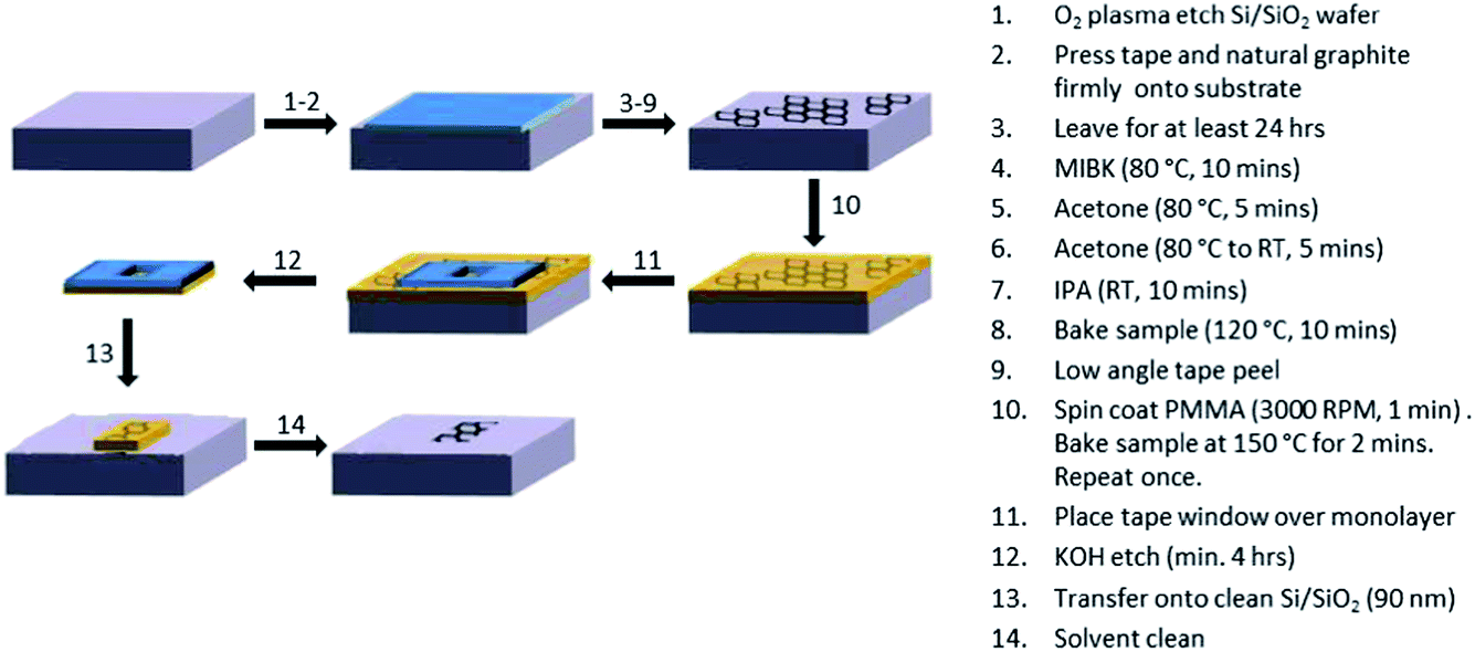 | ||
| Fig. 1 A schematic to show the preparation of the ME graphene samples and transfer process. | ||
Additional cleaning procedures were investigated: the graphene sample prepared by the “standard” cleaning regime we have previously employed15,22 for electrochemical experiments with ME graphene is denoted sample 1. In this case, the graphene is cleaned for 10 minutes each with acetone and IPA. Sample 2 was exposed to a wider range of solvents previously reported in the literature for PMMA removal:18,19,23 successive washes in acetone for 16 h each and IPA (10 min); an overnight acetic acid wash with a 10 minute IPA rinse; and finally a 60 min chloroform wash with a 10 min IPA rinse, with Raman spectroscopy and atomic force microscopy (AFM) performed following each washing stage. As noted in the Introduction, vacuum annealing of graphene samples has been reported as a clean-up protocol:20,23-27 vacuum baking at 215 °C for 16 hours at 10−5 mbar is denoted sample 3, whereas sample 4 was exposed to an ultra-high vacuum (10−9 mbar, 50 °C (2 h), 101 °C (3 days)). Sample 5 was also annealed, but in this case a H2–Ar28–30 (10% H2) environment was used: the sample was heated from room temperature to 50 °C (ramping at 5 °C min-1) held for 1 h, ramped to 110 °C (held for 1 h), then heated to 250 °C (held for 4 h), and subsequently 270 °C (for 7 h).
After the various cleaning procedures, electrical contacts were made to the graphene flakes using silver epoxy (RS components) to connect to copper wire (Advent, UK). All samples were stored in glass Petri dishes to avoid any contaminants previously reported to affect samples when stored in plastic sample boxes.31
Characterisation techniques
Cyclic voltammograms (CV) employed a PGSTAT302N potentiostat (Autolab, UK) using a three electrode set-up where the working electrode (WE) was graphene on Si/SiO2 (samples 1–5), the reference electrode (RE) was a Ag/AgCl wire (Ag wire (Ag coated with PTFE 0.37 mm diameter, Advent, UK) previously anodised in a saturated potassium chloride (Sigma-Aldrich, UK) solution) and the counter electrode (CE) was a Pt wire (0.15 mm diameter, Advent, UK).
A localised electrochemical cell was formed using a droplet, which was held at the end of a pipette as previously reported.15,36 Borosilicate glass capillaries (1.5 mm o.d. × 0.86 mm i.d., Intracel, UK) were pulled (Sutter puller P-97 Flaming/Brown) to a fine tip measuring ca. 1 μm in diameter and were back filled with a solution containing the redox active species and supporting electrolyte, using a syringe and micro-filler (World Precision Instruments, USA). The RE and CE were placed inside the pipette, which was then positioned close to the WE (the ME graphene) using a motorised manipulator (Siskiyou MX7630) before a droplet was formed and held between the WE and the pipette with the aid of a micro-injector (PV820 Pneumatic PicoPump, World Precision Instruments, USA). The sample was placed on the stage of the optical microscope mentioned above (GXML3030 Upright Materials Microscope, attached to a GXCAM-9 camera), hence the pipette was placed at a low (ca. 45°) angle with respect to the microscope stage.
Results & discussion
Sample characterisation
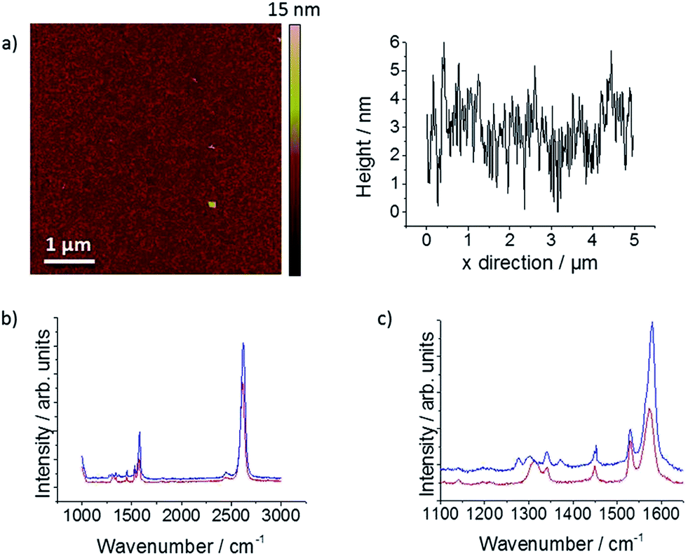
Representative optical micrographs of mechanically-exfoliated (ME) graphene flakes, transferred to a Si/SiO2 wafer, are shown in Fig. 2. Exfoliation of natural graphite typically gives flakes with dimensions in the 0.1–1 mm range. Although the micrographs (Fig. 2(a) and (b)) suggest that the sample shown is continuous, dark-field imaging of the sample reveals wrinkles and defects, introduced during the transfer process. The samples are ultimately contacted and “spotted” with droplets of electrolyte solution containing one of the redox mediators (shown in Fig. 2(d)), which make local electrochemical cells (vide infra). Imperfections in the sample are more readily seen using AFM, as shown in Fig. 3, which shows micrographs and corresponding line profiles from a ME sample washed with different organic solvents, which have each been reported as useful for PMMA removal.18-21 It is clear from Fig. 3(a) that the “default” acetone/IPA wash leaves considerable quantities of contaminant across the sample; this is attributed to PMMA residue that is not removed during the transfer process. The solvent treatments shown successively in Fig. 3 reveal improvements on the acetone/IPA wash: a prolonged acetone treatment, followed by an IPA rinse (Fig. 3(b)), an acetic acid wash for 16 hours followed by a 10 minute IPA rinse (Fig. 3(c)) and a 60 minute chloroform wash, followed by a 10 minute IPA rinse (Fig. 3(d)). The acetone/acetic acid/chloroform treatment in particular has removed much of the polymer residue. Raman spectra from the solvent treated samples are shown in Fig. 4. The 2D peak position (close to 2625 cm−1 in each case) confirms that the graphene is a monolayer, while the upshift of the G peak in the acetone and, particularly, the chloroform treated cases is indicative of sample doping (G peak positions of 1579.6 ± 2.4 cm−1 and 1583.9 ± 2.5 cm−1, respectively). Vacuum annealing of a separate graphene sample, in contrast, gave unsatisfactory results (see Fig. 5). AFM indicated that the sample was largely free of debris, to a scale which was at least as good as the chloroform-washed sample of Fig. 3, however the Raman spectrum had degraded from the pristine monolayer response, with new bands at 1322 cm−1 and 2461 cm−1, which indicate defect formation and sample contamination, respectively. The optical micrograph shown in Fig. 5(d) reveals that distinct fractures in the monolayer have formed on vacuum exposure, which we attribute to “degassing” of solvent residues or gases trapped between the monolayer and the substrate, possibly exacerbated by differential thermal expansion of the ME graphene and the wafer substrate during the heating process. The ultra-high vacuum annealing method was found, via AFM, to yield higher levels of contaminant on the graphene electrode, most likely as a result of contaminants in the chamber (data not shown). Finally, the H2–Ar annealing was found to give some improvement in residue in the AFM, although the Raman spectra (Fig. 6) again showed evidence of sample degradation, suggestive of amorphous carbon contamination or hydrogenation of either the PMMA residues or the graphene itself.24,37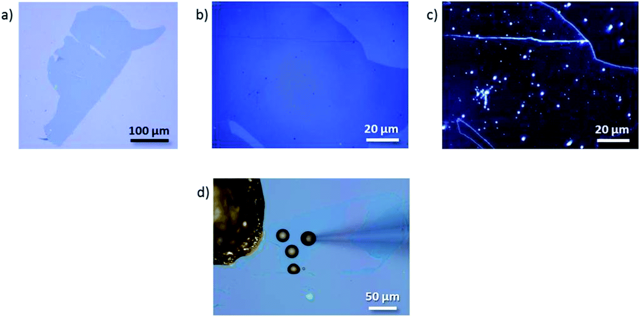 | ||
| Fig. 2 Optical microscopy images of mechanically exfoliated (ME) graphene. Brightfield images show (a) a monolayer flake, (b) a selected area of the flake, (c) a darkfield image showing the same selected area, (d) the electrochemical set-up. | ||
 | ||
| Fig. 3 AFM height images with a corresponding line profile (from centre) showing residue removal from different wet cleaning methods: (a) acetone (10 min), IPA (10 min), (b) successive washes in acetone, acetone (16 h), IPA (10 min), (c) acetic acid (16 h), (d) chloroform (60 min), IPA (10 min). | ||
 | ||
| Fig. 4 (a) Raman spectra after different wet cleaning procedures: acetone (16 h), IPA (10 min) (red); acetic acid, IPA (10 min) (green); chloroform (60 min), IPA (10 min) (black). (b) Enlargement of the wavenumber region where the D and G peaks occur. | ||
 | ||
| Fig. 5 (a) AFM height image with (b) corresponding line profile; (c) the Raman spectrum and (d) optical micrograph of a monolayer ME graphene flake after being vacuum annealed at ca. 10−5 mbar, 215 °C (16 h). | ||
 | ||
| Fig. 6 (a) AFM height image with corresponding line profile of ME graphene after annealing in the presence of H2–Ar at 270 °C (7 h), (b) Raman spectra after annealing at 250 °C (4 h) (red), and 270 °C (7 h) (blue). | ||
Electrochemical response
The voltammetric response of each of the samples was recorded, using the microdroplet approach, with Ru(NH3)63+ and FcTMA+, which are both quoted to be model, outer-sphere redox couples. Droplets of 20–30 μm diameter were employed in this configuration, with the electrolyte contacted within the pipette containing the counter and reference electrodes. This size of droplet is small enough to contact the basal plane of the graphene, avoiding any cracks in the sample, see Fig. 2(d), but large enough to allow the response within the droplet to be approximated as a linear diffusive one, at least for short timescales. The sample prepared via the H2–Ar annealing process (sample 5) was found to be inactive, which is attributed to problems with the contact made to the sample due to extensive cracking of the monolayer (detected using dark-field microscopy). Reproducible voltammetric responses were, however, obtained with both redox couples using the remaining four samples, i.e. numbers 1–4. The rate of electron transfer for both redox couples was found from the dependence of the forward and reverse peak separations over a range of scan rates, for microdroplets deposited at various locations on the graphene samples. When employing FcTMA+/2+ as the redox couple the Nicholson method of analysis was used to determine the electron transfer kinetics.38,39 However, when employing Ru(NH3)63+/2+ as the redox couple the Klingler–Kochi method was preferred due to the large peak separations.40 The kinetics were generally found to be close to the reversible limit for droplets of ca. 20–30 μm diameter (averaged data for several droplets for sample 1: 1.89 (±0.99) × 10−2 cm s−1, sample 2: 2.76 (±1.59) × 10−2 cm s−1, sample 3: 1.09 (±0.99) × 10−2 cm s−1, sample 4: 1.24 (±1.52) × 10−2 cm s−1) when employing FcTMA+ as the redox couple, making it harder to discriminate between intrinsic variations in electrochemical activity between each sample. Note that the kinetics were close to the reversible limit measurable with this system, hence the relatively large error in the rate constants quoted. Representative voltammetry of the FcTMA+ couple obtained from samples 1 and 3 is shown in Fig. 7.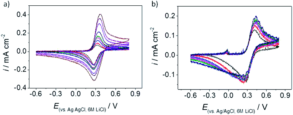 | ||
| Fig. 7 Representative voltammetry obtained for the FcTMA+ couple on (a) sample 1 (default solvent wash), and (b) sample 3 (vacuum annealed). Scan rates: 0.1, 0.15, 0.2, 0.25, 0.3, 0.4, 0.6, 0.8 and 1.0 V s−1. Note the difference in current density for sample 3, which is half of that of sample 1. This is most likely due to a droplet being placed over a crack in the flake that is not visible using the optical microscope (crack size < 1 μm). | ||
The electrochemical behaviour observed for the FcTMA+ couple, with fast electron transfer kinetics, is entirely consistent with that observed previously for this couple on carbon nanotubes.33,41–43 To the best of our knowledge, there has only been one other study investigating this couple on graphene surfaces,35 in this case using CVD graphene. The kinetics of FcTMA+ electron transfer on the CVD sample were probed using an electrochemical microscopy technique with a higher mass transport rate, and therefore a higher upper bound to the range of measureable electron transfer rate constants. The authors of the earlier study reported a standard rate constant for the FcTMA+ couple that is close to the one reported here for monolayer samples of CVD graphene, although the rate of electron transfer was found to increase with an increasing number of CVD layers. In a separate study, the oxidation of another water-soluble ferrocene derivative (ferrocenemethanol) has been reported to be fast, i.e. at the upper bound of the measurement techniques used, on both ME graphene, and on graphene samples derived from chemical vapour deposition (CVD).44 As an outer-sphere redox couple, the FcTMA+ response would be expected to be independent of surface state, and only sensitive to the level of sample doping, however given the fast exchange kinetics for this couple, it seems that any changes in doping due to the different cleaning regimes adopted herein do not significantly affect the measured voltammetry for this molecule.
By contrast, the data in Fig. 8 shows that the kinetics of Ru(NH3)63+/2+ reduction/re-oxidation were substantially slower on the graphene samples (sample 1: 2.87 (±2.90) × 10−5 cm s−1, sample 2: 1.46 (±0.69) × 10−7 cm s−1, sample 3: 3.60 (±4.79) × 10−6 cm s−1, sample 4: 4.42 (±3.07) × 10−7 cm s−1); these values are somewhat slower than the behaviour reported previously for this couple on the basal plane of graphite. Quasi-reversible kinetics with a relatively slow standard electron transfer rate of 1 × 10⁻³ cm s−1, have been reported for Ru(NH3)63+/2+ on basal plane highly oriented pyrolytic graphite.45,46 The kinetics of this redox couple have also been investigated on electrodes modified with commercial CVD graphene samples, although it has been implicitly assumed that the basal plane of the graphene is inactive with respect to electron transfer in this case.47 The slower electron transfer kinetics for Ru(NH3)63+/2+ relative to the reported values for basal plane graphite also, in contrast to the FcTMA+ case, manifest themselves in a slight variation of the standard rate constant with sample pre-treatment, with sample 2 displaying slower kinetics than the other wet cleaned sample, sample 1. One explanation for this is that the doping seen with sample 2 (see Fig. 4) has shifted the Fermi level for this sample into a region with a lower density of states, although why sample 2 should show slower kinetics for the Ru(NH3)63+/2+ case, and not for the FcTMA+ case, is not immediately clear.
 | ||
| Fig. 8 Representative voltammetry obtained for the Ru(NH3)63+ couple on (a) sample 1 (default solvent wash), and (b) sample 3 (vacuum annealed). Scan rates: 0.1, 0.15, 0.2, 0.25, 0.3, 0.4, 0.6, 0.8 and 1.0 V s−1. | ||
Conclusion
Measurable electron transfer kinetics are observed on graphene samples for both mediators in this study, which indicates that the basal plane of this material is electrochemically active. With regard to the specific aim of the work, the main finding is a rather limited sensitivity of the electron transfer kinetics to the specific pre-treatment regime of the graphene electrode. Whereas the presence of polymer and solvent residue, and the associated changes in doping, have been shown to have a substantial effect on the transport properties of graphene samples,18 the electron transfer data appears to be relatively insensitive to the state of the sample surface, at least for the case of the most common contaminant encountered with exfoliated graphene, namely PMMA residue from the transfer process. As well as the variations in doping induced by the different sample treatments, one might expect the different residual levels of adsorbates to influence the rate of electron transfer, not least by blocking significant fractions of the sample surface (see Fig. 3, 5 and 6), given that the deleterious effects of surfactants on the electrochemical response of CVD graphene samples have been noted previously,48 as has the effect of sample “ageing” on the response of graphite electrodes.49 However such variations are not large for the sample treatments attempted here.Acknowledgements
We thank the EPSRC (grants EP/I005145/1, EP/K039547/1 and EP/K016954/1) for financial support and Dr M Bissett for useful discussions.References
- Z. Bo, Z. Wen, H. Kim, G. Lu, K. Yu and J. Chen, Carbon, 2012, 50, 4379 CrossRef CAS PubMed.
- M. F. El-Kady, V. Strong, S. Dubin and R. B. Kaner, Science, 2012, 335, 1326 CrossRef CAS PubMed.
- M. M. Hantel, T. Kaspar, R. Nesper, A. Wokaun and R. Kötz, Electrochem. Commun., 2011, 13, 90 CrossRef CAS PubMed.
- J. Liu, M. Notarianni, G. Will, V. T. Tiong, H. Wang and N. Motta, Langmuir, 2013, 29, 13307 CrossRef CAS PubMed.
- D. Chen, H. Zhang, Y. Liu and J. H. Li, Energy Environ. Sci., 2013, 6, 1362 CAS.
- N. G. Sahoo, Y. Z. Pan, L. Li and S. H. Chan, Adv. Mater., 2012, 24, 4203 CrossRef CAS PubMed.
- H. J. Choi, S. M. Jung, J. M. Seo, D. W. Chang, L. M. Dai and J. B. Baek, Nano Energy, 2012, 1, 534 CAS.
- G. Kucinskis, G. Bajars and J. Kleperis, J. Power Sources, 2013, 240, 66 CrossRef CAS PubMed.
- L. Wang, A. Ambrosi and M. Pumera, Angew. Chem., Int. Ed., 2013, 52, 13818 CrossRef CAS PubMed.
- J. Xia, F. Chen, J. Li and N. Tao, Nat. Nanotechnol., 2009, 4, 505 CrossRef CAS PubMed.
- M. D. Stoller, C. W. Magnuson, Y. Zhu, S. Murali, J. W. Suk, R. Piner and R. S. Ruoff, Energy Environ. Sci., 2011, 4, 4685 CAS.
- X. Li, W. Cai, J. An, S. Kim, J. Nah, D. Yang, R. Piner, A. Velamakanni, I. Jung, E. Tutuc, S. K. Banerjee, L. Colombo and R. S. Ruoff, Science, 2009, 324, 1312 CrossRef CAS PubMed.
- K. S. Novoselov, A. K. Geim, S. V. Morozov, D. Jiang, Y. Zhang, S. V. Dubonos, I. V. Grigorieva and A. A. Firsov, Science, 2004, 306, 666 CrossRef CAS PubMed.
- D. A. C. Brownson and C. E. Banks, Phys. Chem. Chem. Phys., 2012, 14, 8264 RSC.
- P. S. Toth, A. T. Valota, M. Velicky, I. A. Kinloch, K. S. Novoselov, E. W. Hill and R. A. W. Dryfe, Chem. Sci., 2014, 5, 582 RSC.
- A. Das, S. Pisana, B. Chakraborty, S. Piscanec, S. K. Saha, U. V. Waghmare, K. S. Novoselov, H. R. Krishnamurthy, A. K. Geim, A. C. Ferrari and A. K. Sood, Nat. Nanotechnol., 2008, 3, 201 CrossRef PubMed.
- F. Chen, Q. Qing, J. Xia, J. Li and N. Tao, J. Am. Chem. Soc., 2009, 131, 9908 CrossRef CAS PubMed.
- J. W. Suk, W. H. Lee, J. Lee, H. Chou, R. D. Piner, Y. Hao, D. Akinwande and R. S. Ruoff, Nano Lett., 2013, 13, 1462 CAS.
- M. Her, R. Beams and L. Novotny, Phys. Lett. A, 2013, 377, 1455 CrossRef CAS PubMed.
- A. Pirkle, J. Chan, A. Venugopal, D. Hinojos, C. W. Magnuson, S. McDonnell, L. Colombo, E. M. Vogel, R. S. Ruoff and R. M. Wallace, Appl. Phys. Lett., 2011, 99, 112108 CrossRef PubMed.
- C.-J. Shih, Q. H. Wang, S. Lin, K.-C. Park, Z. Jin, M. S. Strano and D. Blankschtein, Phys. Rev. Lett., 2012, 109, 176101 CrossRef.
- A. T. Valota, I. A. Kinloch, K. S. Novoselov, C. Casiraghi, A. Eckmann, E. W. Hill and R. A. W. Dryfe, ACS Nano, 2011, 5, 8809 CrossRef CAS PubMed.
- Z. Cheng, Q. Zhou, C. Wang, Q. Li, C. Wang and Y. Fang, Nano Lett., 2011, 11, 767 CrossRef CAS PubMed.
- J. Hong, M. K. Park, E. J. Lee, D. Lee, D. S. Hwang and S. Ryu, Sci. Rep., 2013, 3, 2700 Search PubMed.
- R. Zan, C. Muryn, U. Bangert, P. Mattocks, P. Wincott, D. Vaughan, X. Li, L. Colombo, R. S. Ruoff, B. Hamilton and K. S. Novoselov, Nanoscale, 2012, 4, 3065 RSC.
- Z. H. Ni, H. M. Wang, Z. Q. Luo, Y. Y. Wang, T. Yu, Y. H. Wu and Z. X. Shen, J. Raman Spectrosc., 2010, 41, 479 CrossRef CAS PubMed.
- X. Wang, L. Jinjin, Z. Qing, Z. Yuan and Z. Mengke, Key Eng. Mater., 2013, 562–565, 85 CrossRef PubMed.
- Y. Huang, X. Dong, Y. Shi, C. M. Li, L.-J. Li and P. Chen, Nanoscale, 2010, 2, 1485 RSC.
- A. M. Goossens, V. E. Calado, A. Barreiro, K. Watanabe, T. Taniguchi and L. M. K. Vandersypen, Appl. Phys. Lett., 2012, 100, 073110 CrossRef PubMed.
- R. Raj, S. C. Maroo and E. N. Wang, Nano Lett., 2013, 13, 1509 CAS.
- Z. Li, Y. Wang, A. Kozbial, G. Shenoy, F. Zhou, R. McGinley, P. Ireland, B. Morganstein, A. Kunkel, S. P. Surwade, L. Li and H. Liu, Nat. Mater., 2013, 12, 925 CrossRef CAS PubMed.
- J. L. Conyers and H. S. White, Anal. Chem., 2000, 72, 4441 CrossRef CAS.
- I. Dumitrescu, P. R. Unwin, N. R. Wilson and J. V. Macpherson, Anal. Chem., 2008, 80, 3598 CrossRef CAS PubMed.
- M. N. Szentirmay and C. R. Martin, Anal. Chem., 1984, 56, 1898 CrossRef CAS.
- A. G. Güell, N. Ebejer, M. E. Snowden, J. V. Macpherson and P. R. Unwin, J. Am. Chem. Soc., 2012, 134, 7258 CrossRef PubMed.
- A. T. Valota, P. S. Toth, Y.-J. Kim, B. H. Hong, I. A. Kinloch, K. S. Novoselov, E. W. Hill and R. A. W. Dryfe, Electrochim. Acta, 2013, 110, 9 CrossRef CAS PubMed.
- D. C. Elias, R. R. Nair, T. M. G. Mohiuddin, S. V. Morozov, P. Blake, M. P. Halsall, A. C. Ferrari, D. W. Boukhvalov, M. I. Katsnelson, A. K. Geim and K. S. Novoselov, Science, 2009, 323, 610 CrossRef CAS PubMed.
- R. S. Nicholson, Anal. Chem., 1965, 37, 1351 CrossRef CAS.
- I. Lavagnini, R. Antiochia and F. Magno, Electroanalysis, 2004, 16, 505 CrossRef CAS PubMed.
- R. J. Klingler and J. K. Kochi, J. Phys. Chem., 1981, 85, 1731 CrossRef CAS.
- J. Kim, H. Xiong, M. Hofmann, J. Kong and S. Amemiya, Anal. Chem., 2010, 82, 1605 CrossRef CAS PubMed.
- I. Heller, J. Kong, H. A. Heering, K. A. Williams, S. G. Lemay and C. Dekker, Nano Lett., 2004, 5, 137 CrossRef PubMed.
- T. S. Miller, N. Ebejer, A. G. Guell, J. V. Macpherson and P. R. Unwin, Chem. Commun., 2012, 48, 7435 RSC.
- W. Li, C. Tan, M. A. Lowe, H. D. Abruña and D. C. Ralph, ACS Nano, 2011, 5, 2264 CrossRef CAS PubMed.
- K. R. Kneten and R. L. McCreery, Anal. Chem., 1992, 64, 2518 CrossRef CAS.
- K. K. Cline, M. T. McDermott and R. L. McCreery, J. Phys. Chem., 1994, 98, 5314 CrossRef CAS.
- D. A. C. Brownson, L. J. Munro, D. K. Kampouris and C. E. Banks, RSC Adv., 2011, 1, 978 RSC.
- D. A. C. Brownson, J. P. Metters, D. K. Kampouris and C. E. Banks, Electroanalysis, 2011, 23, 894 CrossRef CAS PubMed.
- A. N. Patel, M. G. Collignon, M. A. O'Connell, W. O. Y. Hung, K. McKelvey, J. V. Macpherson and P. R. Unwin, J. Am. Chem. Soc., 2012, 134, 20117 CrossRef CAS PubMed.
| This journal is © The Royal Society of Chemistry 2014 |