
Performance, morphology and photophysics of high open-circuit voltage, low band gap all-polymer solar cells†
Kedar D.
Deshmukh
a,
Tianshi
Qin
b,
Joseph K.
Gallaher
c,
Amelia C. Y.
Liu
d,
Eliot
Gann
ae,
Kane
O'Donnell
f,
Lars
Thomsen
e,
Justin M.
Hodgkiss
c,
Scott E.
Watkins
b and
Christopher R.
McNeill
*a
aDepartment of Materials Engineering, Monash University, Clayton, Victoria 3800, Australia. E-mail: christopher.mcneill@monash.edu
bCSIRO Manufacturing Flagship, Private Bag 10, Clayton South MDC, Victoria 3169, Australia
cMacDiarmid Institute for Advanced Materials and Nanotechnology, Victoria University of Wellington, New Zealand
dMonash Centre for Electron Microscopy and School of Physics, Monash University, Clayton, Victoria 3800, Australia
eAustralian Synchrotron, 800 Blackburn Road, Clayton, Victoria 3168, Australia
fDepartment of Imaging and Applied Physics, Curtin University, Bentley, Western Australia 6102, Australia
First published on 11th November 2014
Abstract
The microstructure and photophysics of low-band gap, all-polymer photovoltaic blends are presented. Blends are based on the donor polymer BFS4 (a dithienyl-benzo[1,2-b:4,5-b]dithiophene/5-fluoro-2,1,3-benzothiadiazole co-polymer) paired with the naphthalene diimide-based acceptor polymer P(NDI2OD-T2). Efficiencies of over 4% are demonstrated, with an open circuit voltage of greater than 0.9 V achieved. Transmission electron microscopy reveals a relatively coarse phase-separated morphology, with elongated domains up to 200 nm in width. Near-edge X-ray absorption fine-structure (NEXAFS) spectroscopy and atomic force microscopy (AFM) measurements reveal that the top surface of BFS4:P(NDI2OD-T2) blends is covered with a pure BFS4 capping layer. Depth profiling measurements confirm this vertical phase separation with a surface-directed spinodal decomposition wave observed. Grazing-incidence wide-angle X-ray scattering (GIWAXS) measurements confirm that BFS4 and P(NDI2OD-T2) are semicrystalline with both polymers retaining their semicrystalline nature when blended. Photoluminescence spectroscopy reveals incomplete photoluminescence quenching with as much as 30% of excitons failing to reach a donor/acceptor interface. Transient absorption spectroscopy measurements also find evidence for rapid geminate recombination.
Broader contextOrganic solar cells require use of both a donor and acceptor to achieve efficient device operation. Traditionally the most efficient cells use a polymer donor and a fullerene acceptor. The use of a polymer acceptor is attractive as it can increase absorption in the active layer and improve morphological stability. The efficiency of so-called all-polymer blends however has lagged that of polymer/fullerene blends. Recently, dramatic increases in the efficiency of all-polymer blends have been witnessed through the partnering of low band-gap donor and acceptor polymers suggesting that all-polymer solar cells can be just as efficient as polymer/fullerene solar cells. Here, a novel high-efficiency all-polymer system is presented with high open circuit voltage. Furthermore the morphology and photophysics of this system are thoroughly investigated revealing that although promising efficiencies are being observed for all-polymer blends, fundamental problems that have plagued earlier all-polymer blends have not fully gone away. |
Introduction
Polymer solar cells utilize a blend of electron-donating and electron accepting materials to achieve efficient photovoltaic energy conversion.1 The use of two semiconducting materials with different electron affinities is necessary to facilitate the dissociation of excitons that are the primary product of photoexcitation.2 The active layer in a polymer solar cell is formed by dissolving the donor and acceptor materials in a common solution and casting a film using spin-coating or one of many printing techniques. Necessary to achieving high efficiency is the formation of a nanoscale phase-separated morphology structured on a length scale similar to the exciton diffusion length to maximize the exciton dissociation efficiency.3,4 In addition to ensuring that photogenerated excitons can diffuse to and dissociate at a donor/acceptor heterojunction, the thin film morphology of the active layer should promote the separation of interfacial electron/hole pairs and their subsequent collection at the device electrodes.The highest efficiency polymer solar cells utilize a low band gap polymer as the donor material and a functionalized fullerene as the acceptor material. Power conversion efficiencies of over 10% have been demonstrated for polymer/fullerene solar cells5,6 with much effort devoted to optimizing cell morphology and device performance.7 So-called all-polymer solar cells utilize semiconducting polymers as both donor and acceptor materials.8 While all-polymer solar cells have historically demonstrated lower efficiencies than polymer/fullerene solar cells, they have the potential advantages of improved morphological stability, greater synthetic flexibility and stronger light absorption by the acceptor phase.9 All-polymer solar cells have attracted renewed attention in recent years following the announcement by the company Polyera of an all-polymer solar cell efficiency of nearly 6.5%.8 A number of research groups have recently reported efficiencies of over 4% (ref. 10–12) with Mori et al. most recently reporting an efficiency of 5.7%.13 Common to these high efficiency all-polymer solar cells is the use of low band gap acceptor polymers utilizing naphthalenediimide or perylenediimide moieties. Equally important to the realization of high efficiency all-polymer solar cells has been the pairing of low band gap donor polymers with low band gap acceptor polymers. The electron accepting naphthalenediimide-based polymer poly([N,N-9-bis(2-octyldodecyl)-naphthalene-1,4,5,8-bis(dicarboximide)-2,6-diyl]-alt-5,59-(2,29-bithiophene)) or P(NDI2OD-T2) in particular has been well-studied in all-polymer solar cells14–21 with the current record efficiency of 5.7% utilizing P(NDI2OD-T2) as the acceptor polymer in blends with the donor polymer PBDTTT-EF-T.13 With this rapid advance in all-polymer solar cell efficiency it is important to characterize the microstructure and photophysics of such systems. In particular previous all-polymer blends have suffered from sub-optimal morphologies9 and rapid geminate recombination14,22 and thus it is important to know to what extent these new systems have overcome such problems. Indeed, these promising efficiencies have led one author to recently state that “there are no fundamental reasons as why all-polymer blends cannot achieve efficiencies of fullerene–polymer devices”8 however the fundamental operating mechanisms and morphology limitations of these high efficiency all-polymer systems have yet to be thoroughly investigated. Additionally, the efficiency of solar cells based on high-electron affinity acceptor polymers such as P(NDI2OD-T2) may be limited by the open-circuit voltage that they can support. Thus finding new donor materials that result in high open-circuit voltages whilst maintaining high external quantum efficiencies is also critical.
In this contribution we report high efficiency all-polymer solar cells based on blends of the acceptor polymer P(NDI2OD-T2) with the donor polymer BFS4,23 see Fig. 1. BFS4 is a novel donor/acceptor co-polymer derived from a tailored, multicomponent acceptor–donor–acceptor (A–D–A) intermediate. BFS4 has a A–D1–A–D2 structure which was found to demonstrate superior device performance in polymer/fullerene blends compared to blends utilizing the corresponding A–D1 or A–D2 donor polymers.23 Using BFS4 as the donor polymer in blends with P(NDI2OD-T2) as the acceptor polymer, we have demonstrated all-polymer solar cells with efficiency >4% and open-circuit voltage of >0.9 V. Additionally, we report on the microstructure and photophysics of this system providing evidence of incomplete exciton dissociation and rapid geminate recombination indicating that these problems that have dogged earlier all-polymer systems have not entirely gone away.
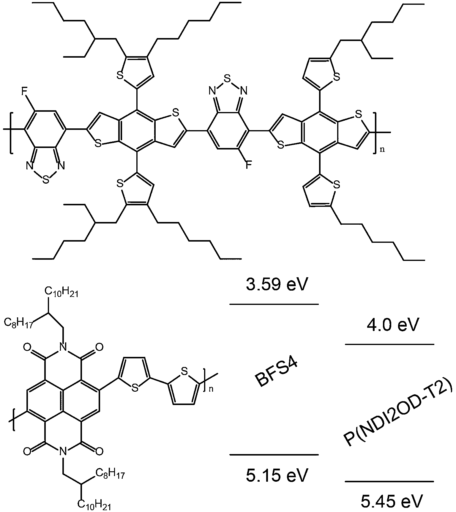 | ||
| Fig. 1 Chemical structures and energy levels of BFS4 and P(NDI2OD-T2). | ||
Results and discussion
Materials
Fig. 1 presents the chemical structures and energy levels of BFS4 and P(NDI2OD-T2). The chemical structure of BFS4 is based on dithienyl-benzo[1,2-b:4,5-b]dithiophene (DT-BDT) and 5-fluoro-2,1,3-benzothiadiazole (FBT) sub-units. Key features of BFS4 are the distinct side chains on the two DT-DBT sub-units in the repeat unit and the orientation of the fluorine atom on the FBT sub-unit with respect to the DT-DBT sub-units. The A–D1–A–D2 structure of BFS4 has been associated with improved supramolecular interactions relative to the corresponding regioregular and random A–D polymers.23 The strong electron withdrawing character of the FBT sub-unit results in a LUMO of −3.6 eV which is deeper than that of other common DBT-based polymers such as PTB719 and PBDTTT-EF-T.13 The HOMO of BFS4 (−5.15 eV) is similar to that of PTB7 and PBDTTT-EF-T resulting in a lower band gap of BFS4 of 1.56 eV compared to other DT-DBT-based polymers. The energy levels of BFS4 are well-matched to P(NDI2OD-T2) with a HOMO/HOMO offset of 0.3 eV and LUMO/LUMO offset of 0.4 eV. Based on the energy levels of Fig. 1 a maximum open-circuit voltage of 1.15 V (calculated as LUMOacceptor–HOMOdonor) is expected.Optical properties
Fig. 2(a) presents the optical absorption spectra of neat films of BFS4 and P(NDI2OD-T2) normalized to film thickness. P(NDI2OD-T2) has a broad near-IR absorption band extending from ∼550 nm to 850 nm and a π–π* absorption feature at 390 nm. BFS4 exhibits more pronounced vibronic features with a sharp absorption peak at ∼675 nm and subsequent peaks at ∼615 nm and 495 nm in the visible along with further peaks in the UV. The higher band-gap of BFS4 provides complementary spectral coverage to P(NDI2OD-T2) providing absorption in between 400 nm and 600 nm where P(NDI2OD-T2) absorption is weak. Normalized to film thickness, BFS4 is more strongly absorbing which may be related to the short alkyl side chains of BFS4 compared to P(NDI2OD-T2) that results in a higher chromophore density. Fig. 2(b) presents the normalized optical absorption spectra of BFS4:P(NDI2OD-T2) blends for different weight ratios. The absorption spectra of the blend track the relative contribution of the two components with the blend spectra well-described by a linear combination of the neat spectra.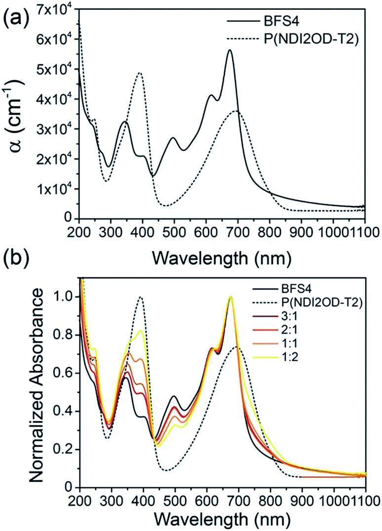 | ||
| Fig. 2 Ultraviolet to near-infrared absorption spectra of (a) neat BFS4 and P(NDI2OD-T2) films and (b) BFS4:P(NDI2OD-T2) blends. | ||
Device performance
Solar cells were fabricated using an inverted architecture consisting of an indium–tin oxide (ITO) glass substrate coated with ZnO and PEIE,24 the BFS4:P(NDI2OD-T2) active layer, a MoOx interfacial layer and top Ag contact (that is, ITO/ZnO/PEIE/BFS4:P(NDI2OD-T2)/MoOx/Ag). Full details of device fabrication and layer thicknesses can be found in the experimental section. Fig. 3 presents device data (external quantum efficiency and current–voltage characteristics) of BFS4:P(NDI2OD-T2) solar cells for different weight ratios. The active layer was spin-coated from a chlorobenzene solution with optimum thickness of ∼105 ± 5 nm. A weight ratio of 2![[thin space (1/6-em)]](https://www.rsc.org/images/entities/char_2009.gif) :1 BFS4:P(NDI2OD-T2) was found to optimize device performance, with external quantum efficiencies over 40%, an open-circuit voltage (VOC) of 0.92 V, fill factor (FF) of 47%, short-circuit current (JSC) of 8.8 mA cm−2 and overall power conversion efficiency (PCE) of 3.9%. The observation that higher loadings of BFS4 are required for optimum performance can be attributed in part to the higher optical absorption strength of BFS4. However it is noted that the fill-factor decreases with increasing P(NDI2OD-T2) content suggesting enhanced morphology-related recombination. Short-circuit current densities were found to agree with the integrated EQE spectra to within 5%. Device parameters are summarized in Table 1, with the error bars for PCE reflecting both variation over multiple batches of devices and the discrepancy between solar simulator and EQE data.
:1 BFS4:P(NDI2OD-T2) was found to optimize device performance, with external quantum efficiencies over 40%, an open-circuit voltage (VOC) of 0.92 V, fill factor (FF) of 47%, short-circuit current (JSC) of 8.8 mA cm−2 and overall power conversion efficiency (PCE) of 3.9%. The observation that higher loadings of BFS4 are required for optimum performance can be attributed in part to the higher optical absorption strength of BFS4. However it is noted that the fill-factor decreases with increasing P(NDI2OD-T2) content suggesting enhanced morphology-related recombination. Short-circuit current densities were found to agree with the integrated EQE spectra to within 5%. Device parameters are summarized in Table 1, with the error bars for PCE reflecting both variation over multiple batches of devices and the discrepancy between solar simulator and EQE data.
 | ||
| Fig. 3 External quantum efficiency, (a), and current–voltage characteristics under simulated sunlight, (b), of BFS4:P(NDI2OD-T2) solar cells as a function of weight ratio. | ||
:P(NDI2OD-T2) solar cells
| Device | J SC (mA cm−2) | V OC (V) | FF | Max. EQE (%) | PCE (%) |
|---|---|---|---|---|---|
| 3:1 |
8.1 | 0.90 | 0.46 | 40 | 3.4 ± 0.2 |
| 2:1 |
8.8 | 0.92 | 0.48 | 43 | 3.9 ± 0.2 |
| 2:1 with 1% DIO |
9.2 | 0.90 | 0.52 | 46 | 4.3 ± 0.2 |
| 1:1 |
8.3 | 0.90 | 0.41 | 41 | 3.1 ± 0.2 |
| 1:2 |
6.0 | 0.88 | 0.34 | 30 | 1.8 ± 0.2 |
Cell efficiency was found to further improve through use of the solvent additive 1,8-diiodooctane (DIO), see Fig. 4. With small amounts of DIO, up to 1% v/v, the overall PCE was found to improve from an average of 3.9% to 4.3%. The main source of this improvement is derived from improvement in cell FF which is found to increase from 0.45 without the solvent additive to 0.52 with 1% DIO. A further increase in FF to 0.54 was observed with an increased DIO concentration of 3% however JSC was found to drop sharply. The most dramatic change in device characteristics with use of the solvent additive is seen in the dark current curves shown in Fig. 4(c). In particular, a close to 2 orders of magnitude drop in dark current is seen for −0.5 < V < 0.5 with use of 3% DIO, where the use of 1% DIO results in a more modest suppression of leakage current. The increase in FF with use of DIO can thus be attributed in part to suppressed dark current.
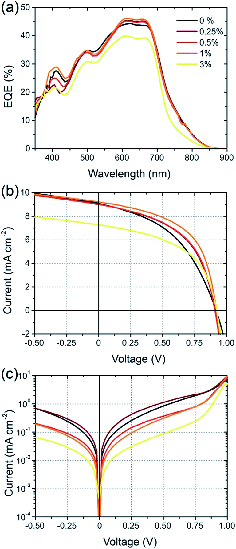 | ||
| Fig. 4 Effect of the solvent additive DIO on the device properties of BFS4:P(NDI2OD-T2) solar cells: (a) EQE spectra; (b) current–voltage characteristics under simulated sunlight; (c) current–voltage characteristics in the dark. | ||
The 4.3% PCE of the BFS4:P(NDI2OD-T2) system is one of the highest reported to date. Especially noteworthy is the open circuit voltage achieved, which is up to 0.92 V. Although other all-polymer systems have achieved open-circuit voltages above 1 V (ref. 19 and 25) to our knowledge this is the highest open-circuit voltage achieved using P(NDI2OD-T2) as acceptor. Initial efforts using P(NDID2OD-T2) as an acceptor in blends with P3HT achieved only modest open-circuit voltages (∼0.5 or less).14,16 It is remarkable that not only has the open-circuit voltage significantly increased when pairing P(NDI2OD-T2) with suitable low band gap donors, but JSC has also significantly increased. The open circuit voltage of over 0.9 V achieved for BFS4:P(NDI2OD-T2) is close to the theoretical maximum of 1.15 V based on the difference between HOMO of BFS4 and the LUMO of P(NDI2OD-T2). The small offset in LUMO and HOMO energies (of order 0.3–04 V) are also close to minimum regarded as being necessary to drive exciton dissociation. The fact that relatively high EQEs can accompany high open circuit voltages for low band gap all-polymer solar cells is encouraging.
Microstructure
To understand structure–function relationships in this novel all-polymer system, the microstructure of BFS4:P(NDI2OD-T2) blends has been probed with a combination of characterization techniques. Atomic force microscopy (AFM) has been employed to image surface topography in combination with transmission electron microscopy (TEM) to image bulk morphology. Synchrotron-based grazing incidence wide-angle X-ray scattering (GIWAXS) was employed to study film crystallinity with near-edge X-ray absorption fine-structure (NEXAFS) spectroscopy used to provide information about surface composition and molecular orientation.
Fig. 5 presents the AFM and TEM images of BFS4:P(NDI2OD-T2) blends. Neat films of BFS4 and P(NDI2OD-T2) exhibit a fibrillar surface morphology (see ESI†) with the neat P(NDI2OD-T2) exhibiting smaller fibrils and a smoother surface topography (RMS roughness of 0.6 nm) than the neat BFS4 film (RMS roughness of 1.9 nm). The surfaces of the blends also exhibit a fibrillar morphology albeit appearing to cover a more nodular underlying morphology. The surface of the blends are also rougher that the neat films, with RMS roughness increasing from 1.1 nm for the 1:2 blend to 1.9 nm for the 1:1 blend and 2.1 nm for the 2:1 blend. A dramatic change in surface morphology is found for the 2:1 film processed with 1% DIO, with the film exhibiting prominent large fibrils with a liquid-crystalline like morphology (surface roughness increases to 6.1 nm). The surface morphology of the 2:1 DIO film closely resembles a neat BFS4 film processed with 1% DIO (see ESI†) suggesting a BFS4-rich surface which was later confirmed by NEXAFS spectroscopy (vide infra). Bright-field TEM images reveal a phase-separated bulk morphology with elongated phases many tens of nanometers in width. Finer-scale fibrillar packing is also observed consistent with that previously observed for neat P(NDI2OD-T2) suggesting a high degree of bulk ordering.26 With increasing BFS4 content, the fraction of the TEM images occupied by the darker phase increases indicating that this darker phase is BFS4-rich. Small isolated black dots are also observed particularly in the blends with majority of P(NDI2OD-T2). Increasing the BFS4 fraction leads to a reduction in the number of these black dots suggesting a better connected morphology for blends with an excess of BFS4. A dramatic change in morphology is also observed with use of the solvent additive DIO with the bulk morphology exhibiting longer range liquid-crystalline order. While the length of the elongated domains is significantly longer for the film processed with DIO, the width of the domains remains similar (∼20–100 nm). Curiously no isolated BFS4 domains (black dots) are observed in the film processed with DIO indicating that DIO is effective in promoting a more bi-continuous morphology. The fact that the domain sizes are much larger than the expected exciton diffusion length of ∼10 nm suggests that incomplete exciton dissociation could be a significant loss mechanism.
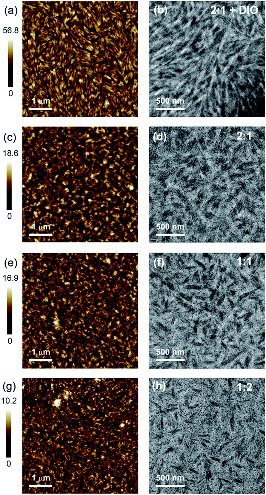 | ||
| Fig. 5 AFM (a, c, e and g) and bright field TEM (b, d, f and h) images of BFS4:P(NDI2OD-T2) blends: 2:1 with 1% DIO, (a) and (b); 2:1, (c) and (d); 1:1 (e) and (f); 1:2 (g) and (h). | ||
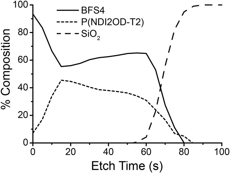
Surface-sensitive NEXAFS spectroscopy was employed to study the chemical composition of the top and bottom surfaces of the blends. The bottom surface was exposed by floating the film off in deionized water and picking it up top–side–down on a silicon substrate. The chemical composition of each surface was determined by fitting the blend spectrum with a linear combination of neat BFS4 and P(NDI2OD-T2) spectra. The average tilt angle of the C 1s → π* transition dipole moment was also determined by measuring the angular dependence of the NEXAFS spectra.27 Further details can be found in the experimental section and in previous work.28Table 2 summarizes the results of the NEXAFS analysis with the NEXAFS spectra used for fitting provided in the ESI.† For all blends examined, irrespective of overall blend composition, a pure BFS4 capping layer is observed; that is, the top surface was found to be pure 100% BFS4 to the limit of instrument sensitivity (1–2%). An edge-on orientation of the BFS4 backbone at the top surface was observed with an average tilt angle of the C 1s → π* transition dipole moment of 〈γ〉 ∼ 70° (where an angle of γ = 90° corresponds to a perfect edge-on orientation). The bottom surface in contrast shows a mixed interfacial composition roughly matching the overall blend ratio. Depth-profiling measurements using a cluster argon ion source in conjunction with X-ray photoelectron spectroscopy confirm the presence of a BFS4-rich capping layer at the top surface. Fig. 6 shows the composition profile for the 2:1 blend with a surface-directed spinodal wave similar to that observed for other OPV blends.29,30 Blends processed with DIO and with different weight ratios show similar composition, see ESI.†
:P(NDI2OD-T2) blends
| Sample | Top | Bottom | ||
|---|---|---|---|---|
| % BFS4 | 〈γ〉 | % BFS4 | 〈γ〉 | |
| Neat BFS4 | 100 ± 1 | 69.6 ± 2.7 | 100 ± 1 | 48.7 ± 0.6 |
| 3:1 |
100 ± 1 | 70.3 ± 0.9 | 64 ± 1 | 50.3 ± 0.6 |
| 2:1 |
100 ± 1 | 69.3 ± 0.7 | 56 ± 1 | 50.7 ± 0.6 |
| 2:1 1% DIO |
98 ± 2 | 69.3 ± 2.4 | 63 ± 1 | 50.6 ± 0.6 |
| 1:1 |
100 ± 1 | 70.0 ± 0.9 | 49 ± 1 | 50.9 ± 0.7 |
| 1:2 |
100 ± 1 | 68.6 ± 1.2 | 31 ± 1 | 49.9 ± 0.9 |
| Neat P(NDI2OD-T2) | 0 | 60.7 ± 0.5 | 0 | 48.0 ± 1.0 |
 | ||
| Fig. 6 Composition as a function of depth for a 105 nm thick BFS4:P(NDI2OD-T2) with 2:1 weight ratio. | ||
Fig. 7 presents the two-dimensional GIWAXS images and pole figures of the 100 (alkyl stacking) peaks, of neat BFS4, neat P(NDI2OD-T2) and the 2:1 blend prepared with and without the solvent additive DIO. Table 3 presents the peak fitting results for the out of plane π-stacking and in-plane alkyl stacking peaks. Strong scattering peaks from both BFS4 and P(NDI2OD-T2) neat films reveal a semicrystalline morphology consistent with previous reports.23,31 Neat BFS4 shows a (100) reflection at q = 0.2902 ± 0.0002 Å−1 consistent with a lamellar stacking distance of ∼2.165 ± 0.002 nm while P(NDI2OD-T2) exhibits a (100) reflection at q = 0.2294 ± 0.0002 Å−1 corresponding to a slightly larger lamellar stacking distance of ∼2.42 ± 0.002 nm. The (100) reflection of BFS4 exhibits a broad orientation distribution indicating a slight preference for face-on packing in the bulk of the film. P(NDI2OD-T2) in contrast exhibits a strong preference for face-on packing of crystallites with the (100) reflection observed predominantly in-plane (polar angles of ±90 degrees). π-stacking peaks for both polymers are largely out of plane, agreeing with both polymers stacking largely in a face-on orientation. Backbone repeat peaks are also observed for both polymers which is characteristic of well-ordered semi rigid conjugated polymers. The GIWAXS pattern of the 2:1 blend prepared without DIO resembles the scattering patterns of the individual components indicating that the polymers are crystallizing in a similar manner in the blend. Unfortunately, the scattering peaks are too close together and overlapping to easily distinguish the individual crystallinities. Scattering from the 2:1 blend prepared without DIO is consistent with the preferential orientation from the neat films being preserved with face-on orientation of P(NDI2OD-T2) and mixed orientation of BFS4. The 2:1 blend prepared with 1% DIO is consistent with an increase in the population of edge-on BFS4 crystallites and a slight increase in overall crystallinity consistent with the effect of DIO on neat films of BFS4 (see ESI†).
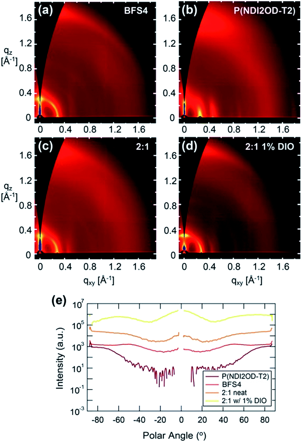 | ||
| Fig. 7 Two-dimensional GIWAXS images of neat BFS4, (a), neat P(NDI2OD-T2), (b), a 2:1 blend of BFS4:P(NDI2OD-T2), (c), and a 2:1 blend of BFS4:P(NDI2OD-T2) prepared with 1 vol% DIO, (d). Figure part (e) shows polar plots of all samples at the 100 peak location. | ||
| In plane 100 peak | Out of plane Pi–Pi stacking peak | |||||
|---|---|---|---|---|---|---|
| D spacing nm | Coherence length nm | Area | D spacing nm | Coherence length nm | Area | |
| BFS4 | 2.165 ± 0.002 | 14.0 ± 0.2 | 200 ± 3 | 0.3783 ± 0.0001 | 3.73 ± 0.04 | 79 ± 1 |
| P(NDI2OD-T2) | 2.422 ± 0.002 | 11.3 ± 0.1 | 493 ± 4 | 0.4063 ± 0.0001 | 3.29 ± 0.04 | 79 ± 2 |
| 2:1 |
2.262 ± 0.002 | 11.3 ± 0.1 | 297 ± 4 | 0.3851 ± 0.0001 | 3.36 ± 0.03 | 91 ± 2 |
| 2:1 DIO |
2.255 ± 0.002 | 19.0 ± 0.2 | 213 ± 3 | 0.3854 ± 0.0001 | 4.16 ± 0.04 | 79 ± 1 |
Photophysics
The photophysics of BFS4:P(NDI2OD-T2) blends has been probed with steady-state photoluminescence and transient absorption spectroscopy. Fig. 8 presents the steady-state photoluminescence of BFS4:P(NDI2OD-T2) blends compared to that of neat BFS4 and P(NDI2OD-T2) polymer films. Films were excited at 620 nm and the spectra have been corrected for detector response and for differences in the number of absorbed photons (resulting from differences in optical density at 620 nm). Neat BFS4 exhibits emission from 700 nm to past 850 nm with characteristic peaks at ∼730 nm and ∼800 nm. P(NDI2OD-T2) exhibits a weaker photoluminescence signal which extends from ∼800 nm out to past 1100 nm.19 BFS4:P(NDI2OD-T2) blends exhibit quenching of both BFS4 and P(NDI2OD-T2) emission consistent with exciton dissociation due to both electron transfer and hole transfer. Photoluminescence quenching is not complete, with the emission of BFS4 in the 2:1 blend only quenched by ∼70%. Blends with a higher fraction of P(NDI2OD-T2) show an apparent increase in quenching of BFS4 emission however this is likely due to the reduced BFS4 content with both BFS4 and P(NDI2OD-T2) absorbing at the pump wavelength. Indeed, the relative amount of photoluminescence at 850 nm, where P(NDI2OD-T2) emits, increases with increasing P(NDI2OD-T2) content. We also note the possibility of energy transfer from BFS4 to P(NDI2OD-T2) that could cause the P(NDI2OD-T2) emission in the blend to appear stronger than expected. In any case, the significant residual emission from the blends indicates that a significant fraction of excitons (of the order of 30% or higher) are not being dissociated at interfaces. Such incomplete exciton dissociation is consistent with the observed morphological characterization with domains of width 20–100 nm.
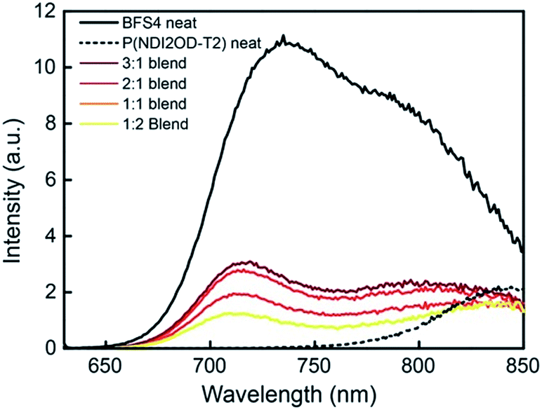 | ||
| Fig. 8 Steady-state photoluminescence spectra of neat BFS4, neat P(NDI2OD-T2) and BFS4:P(NDI2OD-T2) blends. Excitation was at 620 nm and the photoluminescence intensity has been corrected. | ||
Further insight into the kinetics of charge generation and recombination are provided by transient absorption (TA) measurements. Fig. 9 shows the TA spectra of the two neat polymers, conducted at sufficiently low fluence to avoid annihilation effects. In the case of BFS4, the spectra are dominated by two features; a strong ground-state bleach (GSB) feature mirrors the vibronic progression in the linear absorption spectrum at ∼690 nm and ∼615 nm, and a photoinduced absorption (PIA) peak emerges at ∼1300 nm. A weak stimulated emission feature around 800 nm confirms the presence of excitons, and the commensurate decay of all features confirms that a single excitonic species dominates, with a half-life of approximately 80 ps (inset). In the case of P(NDI2OD-T2), the GSB feature peaked at ∼700 nm is accompanied by PIA features at ∼840 nm and ∼1100 nm. The lower energy peak was not observed in previous measurements with a more limited spectral range,14 Combined with the lack of stimulated emission, this may indicate greater charge-separated character in the exciton. Again, all peaks decay on the same time scale, with a half-life of approximately 80 ps (inset).
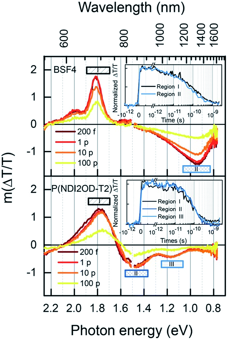 | ||
| Fig. 9 Spectral slices at indicated times of transient absorption measurements on neat polymer films, (top) neat BFS4, (bottom) neat P(NDIOD-T2). Insets show kinetics over the regions specified, normalized by the average value within the first picosecond. | ||
Having established the exciton spectra and lifetimes for both polymers, the dynamics of the blends in the low fluence regime is considered, as shown in Fig. 10. The 532 nm excitation pulse is absorbed mostly (89%) by the BFS4 component, resulting in an initial TA spectrum (Fig. 10(a)) resembling the BFS4 exciton. However, the ratio of the exciton PIA at 1300 nm to the GSB peak at 690 nm is less than half of that in the neat polymer. Considering that charge pairs will retain the GSB peak, this suggests that over 50% of excitons are converted to charges within the first 200 fs. Consistent with this interpretation is the absence of net stimulated emission on the ultrafast timescale due to overlapping PIA from promptly generated charges. The progression of TA spectra reveal the subsidence of the exciton PIA peak to leave a flat PIA feature extending from ∼720 nm into the near IR, with a small peak at 1000 nm. The resulting spectrum is consistent with the formation of charge pairs.22 Although spectral features associated with P(NDI2OD-T2) are not explicitly resolved, this is presumably due to their lower oscillator strength. Energy transfer from BFS4 to the lower bandgap polymer P(NDI2OD-T2) is also possible, however, this does not appear to play a major role based on the retention of the BFS4-based GSB when the exciton PIA peak decays.
 | ||
| Fig. 10 Transient absorption measurements of a 2:1 blend (BFS4:P(NDI2OD-T2)) thin film. (a) Spectral slices at indicated times, (b) kinetics of the regions specified, inset shows the charge recombination kinetics integrated over region I, normalized by the average value within the first picosecond. | ||
Fig. 10(b) shows the kinetics for various wavelength regions indicated on the spectra, allowing us to draw several conclusions about photocurrent losses in the active layer. Beyond the prompt reduction in the BFS4 exciton PIA peak noted above, its subsequent decay (region III) is only slightly faster than the neat polymer, with a half-life of approximately 20 ps. This suggests that a large fraction of excitons are formed too far from interfaces to contribute photocurrent, consistent with the high levels of residual photoluminescence measured. Region II tracks the charge population via the PIA around 1000 nm. Accounting for the fact that approximately one quarter of the signal amplitude is due to the overlapping edge of the exciton PIA, we nevertheless see that charges do not substantially outlive excitons. Charges begin recombining after just 10 ps, leaving only 30% of the initial charge yield by 2 ns. Little change in the dynamics is seen with increasing pump fluence (see Fig. S6 in the ESI†) confirming that measurements were performed in the linear regime with minimal exciton charge annihilation. The GSB decay (region I) tracks the charge PIA (region II), since the GSB probes the total population of excitations, confirming rapid geminate recombination to the ground state. The inset of Fig. 10(b) extends the GSB probe into the microsecond regime, where free charge carriers are available as extractable photocurrent. We find that this recombination phase is also substantially faster than polymer–fullerene blends,32 with most charges recombining within tens of nanoseconds and very few surviving beyond 1 μs. This decay is further accelerated via bimolecular charge recombination at higher fluences (see Fig. S7 in the ESI†). The dynamics of other blend ratios and 2:1 blends prepared with DIO were found to be very similar.
From the above analysis, it is clear that despite the significant improvement in the efficiency of BFS4:P(NDI2OD-T2) solar cells compared to earlier generation all-polymer blends (such as P3HT:F8TBT, P3HT:P(NDI2OD-T2)) many of the limiting characteristics of polymer/polymer blends still remain. In particular, rapid geminate recombination is still observed indicating that charge separation is not as efficient as in polymer/fullerene solar cells which likely explains why current state-of-the-art all-polymer solar cells still exhibit lower fill-factors than polymer/fullerene solar cells. Film morphology is also still an issue. From the transient absorption measurements, evidence of rapid charge generation indicates significant intermixing within the large domains. The residual photoluminescence is then likely to originate from crystallites that are embedded in the larger meso-scale domains. However, the inability to control domain sizes and domain composition still remains a challenge. An improved understanding of the effect of the solvent additive and moving towards a mechanistic understanding of solvent additives in all-polymer systems (as has been pursued for polymer/fullerene blends) is desirable. Varying the molecular weight of donor and acceptor provides another avenue for tuning domain size and composition. The recent report of P3HT-b-PFTBT block co-polymer solar cells with efficiency higher than that of P3HT:PFTBT blends33 suggests that block co-polymers may be an effective strategy for morphology control in high efficiency all-polymer systems as well.
Finally it is worth reflecting on the properties of the acceptor polymer P(NDI2OD-T2). While P(NDI2OD-T2) has proven to be the most effective polymer acceptor to date, there are properties of P(NDI2OD-T2) that make it less than ideal. One of the motivations for using a polymer acceptor rather than a fullerene acceptor is the increased absorption. However, the relatively low absorption co-efficient of P(NDI2OD-T2) in the near-IR only leads to a modest contribution in photocurrent below the band-gap of BFS4 as shown in Fig. 3. P(NDI2OD-T2) was developed primarily for applications in OFETs and thus its optical properties are not necessarily optimized. One reason already given for its low absorption strength is the long solubilizing side-chains that dilute the chromophores. Assuming that these side-chains could be shortened without affecting processibility would lead to an immediate improvement in cell performance. Alternatively, tuning the properties of the donor/acceptor paring is another strategy for improving the optical properties of the acceptor. In any case, although P(NDI2OD-T2) has become the de-facto standard acceptor for all-polymer solar cells, it should not be regarded as optimal with improvements in device efficiency possible with novel acceptor polymers with superior optical properties.
Conclusions
An efficiency of >4% has been demonstrated for the BFS4:P(NDI2OD-T2) low-band gap, all-polymer system. In particular an open-circuit voltage of >0.9 is demonstrated which is the highest achieved with the acceptor polymer P(NDI2OD-T2). The microstructure and photophysics of this system has been examined in depth indicating that while promising efficiencies are demonstrated, characteristic problems associated with all-polymer blends still remain. In particular, relatively coarse domains are observed with TEM indicating poor morphology control, and rapid geminate recombination is observed with ultrafast transient absorption spectroscopy. The fact that other high-efficiency all-polymer systems exhibit similar fill-factors suggests that the limitations observed in this system are likely to be general and further work is required to realize long-lived charge-separated states in all-polymer blends akin to polymer/fullerene blends. Improved understanding of the factors controlling domain size and the action of solvent additives in all-polymer blends will also assist in advancing this technology.Experimental section
Materials
BFS4 was synthesized as described previously23 with a molecular weight of MW = 140000 g mol−1 and dispersity of Đ = 3.26 as determined by high temperature gel permeation chromatography (GPC). P(NDI2OD-T2) was purchased from Polyera Corporation with MW = 75.3 and Đ = 2.04.
Material characterization
Molecular weights of the polymers were characterized by HT-GPC performed in 1,2,4-trichlorobenzene (TCB) with 500 ppm 3,5-di-tert-butyl-4-hydroxytoluene (1.0 mL min−1) at 120 °C using a Malvern Viscotek 350A HT-GPC system with a Refractive Index Detector, a Viscotek 2600 Photodiode Array Detector, a Viscometry Detector, a series of four Malvern high temperature columns (1 × Guard + 3 × HT6000M), and OmniSEC Software. The GPC was calibrated with narrow polydispersity polystyrene standards (Malvern PolyCal PS standards, MW from 1050 to 4.2 × 10⁶), and molecular weights are reported both polystyrene equivalents based on the refractive index detector, and absolute values using universal calibration based on a combination of the refractive index detector and the viscosity detector. Samples were dissolved in TCB with 500 ppm BHT at a concentration around 2.5 mg mL−1 at 120 °C for 2 hours before injection.UV-vis absorption spectra were collected on an Agilent 8453 UV-Visible spectrophotometer over the range 220–1100 nm. Photoluminescence spectroscopy was performed on a Horiba Jobin Yvon Fluorolog 3 spectrofluorometer with an excitation wavelength of 620 nm. Surface topography was characterized with a Veeco Nanoscope V atomic force microscope (AFM) using ScanAsyst mode.
Device fabrication
Devices were fabricated with an ITO/ZnO/PEIE/BFS4:P(NDI2OD-T2)/MoOx/Ag geometry. The ITO/glass substrate was first cleaned in acetone for 10 min, followed by cleaning with IPA in an ultrasonic bath. This was followed by oxygen plasma cleaning for 10 min. Approximately 10 nm of zinc oxide was deposited by spin-coating a precursor solution of zinc acetate dihydrate (0.1 M in 2-methoxy methanol with 1:2 zinc–amine ratio) and curing for 30 min at 200 °C. Polyethyleneamine (PEIE) was then spin coated on the cured ZnO film from a 0.4 wt% solution in 2-methoxyethanol and cured at 100 °C for 15 min. A double layer of ZnO + PEIE was found to be more effective than just either of the interlayers. After transferring substrates to a nitrogen glovebox the active layer was then spin coated from chlorobenzene with 1,8-diidooctane used as an optional solvent additive in varying percentages by volume to the blend solution. 15 nm of molybdenum oxide was deposited on the active layer in vacuo followed by 100 nm of Ag. The devices were encapsulated using glass and epoxy adhesive before removal from the glove box for testing.
Device characterization
Device performance under simulated sunlight was performed using a Photo Emission Tech. model SS50AAA solar simulator with the current–voltage curves measured by a Keithley 2635 source meter. The intensity of the solar simulator was set using a calibrated silicon reference cell with a KG3 glass filter (PV Measurements). The output of the solar simulator was characterized with a spectroradiometer (PV Measurements). A spectral mismatch of 1.01 to 1.02 was determined for BFS4:P(NDI2OD-T2) cells. External quantum efficiency (EQE) was measured as a function of wavelength by dispersing light from a tungsten filament (Newport 250 W QTH) through a monochromator (Oriel Cornerstone 130) with a spot size smaller than the device active area. Light intensity of less than 1 mW cm−2 was used with short-circuit current recorded using a Keithley 2635 source measure unit. The system was calibrated by placing a calibrated photodiode (Thorlabs FDS-100CAL) in the device under test position and referencing the intensity measured to that of another silicon photodiode that samples a fraction of the beam.Transmission electron microscopy
TEM measurements were performed at the Monash Centre for Electron Microscopy with a JEOL JEM 2100F FEGTEM operated at 200 kV in bright-field mode using a small (20 μm) objective aperture to enhance mass-thickness contrast with a constant defocus of −10 μm to enhance phase contrast from the phase boundaries.NEXAFS spectroscopy
NEXAFS measurements were carried out at the soft X-ray beamline at the Australian Synchrotron.34 Nearly perfectly linearly polarized photons (P ≈ 1) from an undulator X-ray source with high spectral resolution of E/ΔE ≤ 10000 were focused to a beam size of ∼100 μm onto samples in an ultrahigh vacuum chamber. X-ray absorption was measured via partial electron yield using a channeltron detector. The recorded signal was normalized to the incident photon flux using a gold mesh. The spectra were normalized by setting the pre-edge signal at 280 eV to 0 and normalizing the post-edge signal at 320 eV to 1. Surface composition was determined by fitting blend spectra taken at the so-called magic angle of 55° to neat reference spectra via single-value decomposition. Average tilt angles were determined by measuring angle-dependent NEXAFS spectra and fitting to the expression:where I is the area of the π* manifold, θ is the X-ray incidence angle and γ is the average tilt angle of the carbon 1s to π* transition dipole moment.35
GIWAXS
GIWAXS measurements were performed at the SAXS/WAXS beamline of the Australian Synchrotron.36 9 keV photons were used with 2D scattering patterns recorded on a Pilatus 1M detector. The sample-to-detector distance was calibrated using a silver behenate standard. Scattering patterns were recorded as a function of X-ray angle of incidence, with the angle of incidence varied from 0.05 degrees below the critical angle of the organic film to 0.2 degrees above the critical angle. The images reported were at the critical angle as identified by the angle with the highest scattering intensity. Data acquisition times of 3 s were used, with three 1 s exposures taken with offset detector positions to cover gaps in the Pilatus detector. X-ray diffraction data are expressed as function of the scattering vector, q, that has a magnitude of (4π/λ)sin(θ), where θ is half the scattering angle and λ is the wavelength of the incident radiation.XPS depth profiling
XPS depth profiling was carried out at Curtin University using a Kratos Ultra DLD XPS system equipped with a gas-cluster ion source. Argon ion clusters of mean size 500 atoms and energy 20 kV (40 eV per atom) were used for etching in 15 second increments. At each etch step, core level spectra were acquired for fluorine, sulphur, oxygen, nitrogen, carbon, silicon and iodine using a pass energy of 160 eV, a selected area aperture of 110 micron diameter and an acquisition time between 30–90 seconds. The X-ray source used was a monochromated Al X-ray gun (photon energy 1486.6 eV) at a power of 225 W. No sample damage (e.g. loss of fluorine) was observed after extended exposure under these conditions. Depth profiles were quantified using Kratos Vision 2 software and the Kratos sensitivity factors. Neat films of the component materials were used to calibrate the relative ratios of each element for a given material and decompose the elemental depth profiles of the blends into a compositional depth profile.Transient absorption spectroscopy
All samples were measured under dynamic vacuum (10−5 bar) using a homebuilt sample chamber. Transient absorption (TA) spectroscopy was carried out using an amplified Ti–sapphire laser (Spectra Physics, 100 fs pulse duration, 800 nm, 3 kHz). The broadband probe pulses were generated via two different methods. Visible wavelengths (550–850 nm) were generated using a homebuilt noncollinear optical parametric amplifier (NOPA) based on ref. 37 pumped by a fraction of output from the amplifier. Infrared wavelengths (830–1700 nm) were generated by focusing a small portion of output from the amplifier in a 3 mm YAG window.After transmission through the sample, visible probe pulses were coupled into a spectrograph (Acton SP2150, Princeton Instruments, 150 lines per mm grating) using optical fibres, and referenced to a probe pulse that was not transmitted through the sample. IR probe pulses were transmitted through a 830 nm long pass filter before reaching the sample chamber and then spectrally dispersed using a homebuilt prism based polychromator after transmission through the sample. Probe shots were read out at 3 kHz using a camera controller (Stresing) equipped with a dual channel linear Si photodiode array (visible) and a single channel linear InGaAs photodiode array (IR). The differential transmission signal (ΔT/T) is calculated using sequential probe shots corresponding to pump on vs. off, where the excitation repetition rate is ω/2. In a typical measurement, 2000 shots were averaged per time point and a time series were repeated 5 times.
For ultrafast (<3 ns) measurements, an optical parametric amplifier (TOPAS) provided 100 fs excitation pulses at 532 nm, which were chopped at 1.5 kHz. The excitation beam was attenuated to achieve an excitation intensity of approximately 5 μJ cm−2 for neat BFS4 and blend samples and 15 μJ cm−2 for neat P(NDI2OD-T2), which has a lower absorption cross section at the excitation wavelength. The observation of comparable dynamics up to ∼4-fold higher fluence (Fig. S6 in the ESI†) confirmed bimolecular effects were insignificant on sub-nanosecond timescales at the fluences used here. The relative delay between pump and probe pulses was varied using an automated delay stage (Newport). For charge recombination measurements (ns–ms), excitation pulses were obtained using the 2nd harmonic (532 nm) of a Q-switched Nd:YVO4 laser (AOT-YVO-25QSP, 700 ps) which was synchronized with the amplifier output. Excitation intensities were varied (1.1–11 μJ cm−2) and each measurement were averaged 1000 shots per time point, with the number of repeat scans to achieve sufficient signal–noise and account for signal strength at different intensities. The delay between pump and probe pulses was varied using an electronic delay generator (Stanford Research Systems DG535).
All transient absorption data was processed using MATLAB, starting with chirp correction for ultrafast measurements. Visible and IR components were combined. In the cases where excitation densities were not identical for visible and IR measurements of the same sample, IR spectra were re-scaled by the ratio of excitation fluences used. Observing a smooth transition between data in the visible and IR wavelength ranges after correction verified the validity of this procedure. In normalized kinetics comparisons, kinetic traces were normalized by the average value between 100 fs and 1 ps, rather than the maximum value, to account for noise fluctuations in the signal.
Acknowledgements
This work was supported by the Australian Research Council (FT100100275) and veski. Part of this research was undertaken on the soft X-ray and SAXS/WAXS beamlines at the Australian Synchrotron, Victoria, Australia. Materials and equipment used for this work were also supported by the Victorian Organic Solar Cell Consortium (VICOSC), (Victorian Department of Primary Industries, Victorian Department of Business and Innovation) the Australian Renewable Energy Agency (ARENA) and the Australian Centre for Advanced Photovoltaics (ACAP). This work was performed in part at the Melbourne Centre for Nanofabrication (MCN) in the Victorian Node of the Australian National Fabrication Facility (ANFF).Notes and references
- G. Li, R. Zhu and Y. Yang, Nat. Photonics, 2012, 6, 153 CrossRef CAS.
- P. W. M. Blom, V. D. Mihailetchi, L. J. A. Koster and D. E. Markov, Adv. Mater., 2007, 19, 1551 CrossRef CAS.
- P. K. Watkins, A. B. Walker and G. L. B. Verschoor, Nano Lett., 2005, 5, 1814 CrossRef CAS PubMed.
- B. P. Lyons, N. Clarke and C. Groves, Energy Environ. Sci., 2012, 5, 7657 CAS.
- J. You, C.-C. Chen, Z. Hong, K. Yoshimura, K. Ohya, R. Xu, S. Ye, J. Gao, G. Li and Y. Yang, Adv. Mater., 2013, 25, 3973 CrossRef CAS PubMed.
- C.-C. Chen, W.-H. Chang, K. Yoshimura, K. Ohya, J. You, J. Gao, Z. Hong and Y. Yang, Adv. Mater., 2014, 26, 5670 CrossRef CAS PubMed.
- L. Lu and L. Yu, Adv. Mater., 2014, 26, 4413 CrossRef CAS PubMed.
- A. Facchetti, Mater. Today, 2013, 16, 123 CrossRef CAS PubMed.
- C. R. McNeill, Energy Environ. Sci., 2012, 5, 5653 CAS.
- T. Earmme, Y.-J. Hwang, S. Subramaniyan and S. A. Jenekhe, Adv. Mater., 2014, 26, 6080 CrossRef CAS PubMed.
- Y. Zhou, T. Kurosawa, W. Ma, Y. Guo, L. Fang, K. Vandewal, Y. Diao, C. Wang, Q. Yan, J. Reinspach, J. Mei, A. L. Appleton, G. I. Koleilat, Y. Gao, S. C. B. Mannsfeld, A. Salleo, H. Ade, D. Zhao and Z. Bao, Adv. Mater., 2014, 26, 3767 CrossRef CAS PubMed.
- D. Mori, H. Benten, I. Okada, H. Ohkita and S. Ito, Adv. Energy Mater., 2014, 4, 1301006 Search PubMed.
- D. Mori, H. Benten, I. Okada, H. Ohkita and S. Ito, Energy Environ. Sci., 2014, 7, 2939 CAS.
- J. R. Moore, S. Albert-Seifried, A. Rao, S. Massip, B. Watts, D. J. Morgan, R. H. Friend, C. R. McNeill and H. Sirringhaus, Adv. Energy Mater., 2011, 1, 230 CrossRef CAS.
- T. W. Holcombe, J. E. Norton, J. Rivnay, C. H. Woo, L. Goris, C. Piliego, G. Griffini, A. Sellinger, J.-L. Brédas, A. Salleo and J. M. J. Fréchet, J. Am. Chem. Soc., 2011, 133, 12106 CrossRef CAS PubMed.
- S. Fabiano, Z. Chen, S. Vahedi, A. Facchetti, B. Pignataro and M. A. Loi, J. Mater. Chem., 2011, 21, 5891 RSC.
- M. Schubert, D. Dolfen, J. Frisch, S. Roland, R. Steyrleuthner, B. Stiller, Z. Chen, U. Scherf, N. Koch, A. Facchetti and D. Neher, Adv. Energy Mater., 2012, 2, 369 CrossRef CAS.
- Y. Tang and C. R. McNeill, J. Polym. Sci., Part B: Polym. Phys., 2013, 51, 403 CrossRef CAS.
- N. Zhou, H. Lin, S. J. Lou, X. Yu, P. Guo, E. F. Manley, S. Loser, P. Hartnett, H. Huang, M. R. Wasielewski, L. X. Chen, R. P. H. Chang, A. Facchetti and T. J. Marks, Adv. Energy Mater., 2014, 4, 1300785 Search PubMed.
- H. Yan, B. A. Collins, E. Gann, C. Wang, H. Ade and C. R. McNeill, ACS Nano, 2012, 6, 677 CrossRef CAS PubMed.
- M. Schubert, B. A. Collins, H. Mangold, I. A. Howard, W. Schindler, K. Vandewal, S. Roland, J. Behrends, F. Kraffert, R. Steyrleuthner, Z. Chen, K. Fostiropoulos, R. Bittl, A. Salleo, A. Facchetti, F. Laquai, H. W. Ade and D. Neher, Adv. Funct. Mater., 2014, 24, 4068 CrossRef CAS.
- J. M. Hodgkiss, A. R. Campbell, R. A. Marsh, A. Rao, S. Albert-Seifried and R. H. Friend, Phys. Rev. Lett., 2010, 104, 177701 CrossRef.
- T. Qin, W. Zajaczkowski, W. Pisula, M. Baumgarten, M. Chen, M. Gao, G. Wilson, C. D. Easton, K. Müllen and S. E. Watkins, J. Am. Chem. Soc., 2014, 136, 6049 CrossRef CAS PubMed.
- Y. Zhou, C. Fuentes-Hernandez, J. Shim, J. Meyer, A. J. Giordano, H. Li, P. Winget, T. Papadopoulos, H. Cheun, J. Kim, M. Fenoll, A. Dindar, W. Haske, E. Najafabadi, T. M. Khan, H. Sojoudi, S. Barlow, S. Graham, J.-L. Brédas, S. R. Marder, A. Kahn and B. Kippelen, Science, 2012, 336, 327 CrossRef CAS PubMed.
- C. R. McNeill, A. Abrusci, J. Zaumseil, R. Wilson, M. J. McKiernan, J. J. M. Halls, N. C. Greenham and R. H. Friend, Appl. Phys. Lett., 2007, 90, 193506 CrossRef PubMed.
- C. J. Takacs, N. D. Treat, S. Krämer, Z. Chen, A. Facchetti, M. L. Chabinyc and A. J. Heeger, Nano Lett., 2013, 13, 2522 CrossRef CAS PubMed.
- C. R. McNeill and H. Ade, J. Mater. Chem. C, 2013, 1, 187 RSC.
- T. Schuettfort, L. Thomsen and C. R. McNeill, J. Am. Chem. Soc., 2013, 135, 1092 CrossRef CAS PubMed.
- Y. Vaynzof, D. Kabra, L. Zhao, L. L. Chua, U. Steiner and R. H. Friend, ACS Nano, 2011, 5, 329 CrossRef CAS PubMed.
- Y. Vaynzof, T. J. K. Brenner, D. Kabra, H. Sirringhaus and R. H. Friend, Adv. Funct. Mater., 2012, 22, 2418 CrossRef CAS.
- J. Rivnay, M. F. Toney, Y. Zheng, I. V. Kauvar, Z. Chen, V. Wagner, A. Facchetti and A. Salleo, Adv. Mater., 2010, 22, 4359 CrossRef CAS PubMed.
- A. J. Barker, K. Chen and J. M. Hodgkiss, J. Am. Chem. Soc., 2014, 136, 12018 CrossRef CAS PubMed.
- C. Guo, Y.-H. Lin, M. D. Witman, K. A. Smith, C. Wang, A. Hexemer, J. Strzalka, E. D. Gomez and R. Verduzco, Nano Lett., 2013, 13, 2957 CrossRef CAS PubMed.
- B. C. C. Cowie, A. Tadich and L. Thomsen, AIP Conf. Proc., 2010, 1234, 307 CrossRef PubMed.
- J. Stöhr, NEXAFS Spectroscopy, Springer, Berlin, 1992 Search PubMed.
- N. M. Kirby, S. T. Mudie, A. M. Hawley, D. J. Cookson, H. D. T. Mertens, N. Cowieson and V. Samardzic-Boban, J. Appl. Crystallogr., 2013, 46, 1670 CrossRef CAS.
- C. Manzoni, D. Polli and G. Cerullo, Rev. Sci. Instrum., 2006, 77, 023103 CrossRef PubMed.
Footnote |
| † Electronic supplementary information (ESI) available: ESI includes AFM images of neat films, full NEXAFS spectroscopy data sets and analysis, depth profiling results of other blends, additional GIWAXS results, fluence dependence of decay kinetics. See DOI: 10.1039/c4ee03059a |
| This journal is © The Royal Society of Chemistry 2015 |