Semi-crystalline photovoltaic polymers with efficiency exceeding 9% in a ∼300 nm thick conventional single-cell device†
Received
17th May 2014
, Accepted 19th June 2014
First published on 19th June 2014
Abstract
We report a series of semi-crystalline, low band gap (LBG) polymers and demonstrate the fabrication of highly efficient polymer solar cells (PSCs) in a thick single-cell architecture. The devices achieve a power conversion efficiency (PCE) of over 7% without any post-treatment (annealing, solvent additive, etc.) and outstanding long-term thermal stability for 200 h at 130 °C. These excellent characteristics are closely related to the molecular structures where intra- and/or intermolecular noncovalent hydrogen bonds and dipole–dipole interactions assure strong interchain interactions without losing solution processability. The semi-crystalline polymers form a well-distributed nano-fibrillar networked morphology with PC70BM with balanced hole and electron mobilities (a h/e mobility ratio of 1–2) and tight interchain packing (a π–π stacking distance of 3.57–3.59 Å) in the blend films. Furthermore, the device optimization with a processing additive and methanol treatment improves efficiencies up to 9.39% in a ∼300 nm thick conventional single-cell device structure. The thick active layer in the PPDT2FBT:PC70BM device attenuates incident light almost completely without damage in the fill factor (0.71–0.73), showing a high short-circuit current density of 15.7–16.3 mA cm−2. Notably, PPDT2FBT showed negligible changes in the carrier mobility even at ∼1 μm film thickness.
Broader context
Polymer solar cells (PSCs) have great potential as a promising candidate for clean and renewable energy sources. PSCs are attracting increasing attention from both academia and industry, due to the demand for flexible, portable and solution processable low-cost photovoltaic devices to comply with increasing global energy demand. As results of many efforts for developing PSCs, the power conversion efficiency (PCE) of PSCs has been tremendously improved over the past decades. However, the low PCE is still a hurdle to overcome for commercial applications of PSCs. To further optimize PSCs, several challenges have to be considered including development of highly soluble and crystalline photovoltaic polymers to enable thick film production without damage in the fill factor. In this work, we report a new series of semi-crystalline photovoltaic polymers, demonstrating a clear molecular design strategy, structure–property relationships and the highest PCE of 9.39% (reported so far) in a 290 nm thick single-cell device. We believe that our findings offer a bright future for the large scale commercialization of PSCs into daily-use electronic devices.
|
1. Introduction
Over the past few decades, polymer solar cells (PSCs) have made significant progress, showing their potential in low-cost, flexible, lightweight, portable and large-area energy-harvesting devices.1 Considerable efforts have been dedicated toward the design of new materials, device architectures and processing techniques in order to improve the power conversion efficiency (PCE).2–5 Recently, bulk heterojunction (BHJ) PSCs, consisting of low band gap (LBG) polymers (as an electron donor) mixed with C60 or C70 fullerene derivatives (as an electron acceptor), have shown promising performance with PCEs of 8–9% in single junction devices.6 Cao et al. reported highly efficient (9.2% PCE) inverted-type PSCs based on the benzodithiophene–thienothiophene copolymer (PTB7) with an amine-functionalized polymer interlayer as an indium tin oxide (ITO) surface modifier.7 With regard to a single cell having conventional geometry, Yu et al. further optimized PTB7 by replacing thiophene with thienothiophene in the benzodithiophene moiety to yield a dithieno[2,3-d:2′,3′-d′]benzo[1,2-b:4,5-b′]dithiophene-based polymer (PTDBD2) with a PCE of 7.6%.8 Chou et al. reported a new fluorinated quinoxaline-based copolymer (PBDT-TFQ) showing 8% PCE.9
To further improve PCEs, first and foremost, the molecular structure of LBG polymers should be carefully designed by considering their close relationship with the photovoltaic parameters, including short-circuit current density (JSC), open-circuit voltage (VOC) and fill factor (FF). Recently, highly efficient photovoltaic materials have been designed by introducing fluorine (F) atoms onto the polymeric chain.10,11 Fluorine has a small van der Waals radius (∼1.35 Å) and is the most electronegative element with a Pauling electronegativity of 4.0. The introduction of fluorine onto the periphery of an electron-deficient unit is a versatile strategy, because it not only minimizes any undesired steric hindrance along the polymer chains but also effectively stabilizes the highest occupied molecular orbital (HOMO) and lowest unoccupied molecular orbital (LUMO) levels. Furthermore, hole mobility improves upon fluorination, though a reverse trend has been observed in some cases.12 The fluorine substituent often has a great influence on inter- and intramolecular interactions,13–15 which play important roles in the solid-state polymer organization with a cofacial π–π stacking. An effective approach to planarize a polymer chain (without losing its solution processability) is to create a noncovalent attractive interaction between neighboring moieties via intramolecular hydrogen bonds, dipole–dipole interactions, etc. Noncovalent intramolecular O⋯S interactions between alkoxy substituents and thiophene rings have been demonstrated to be effective for minimizing torsional angles within polymer backbones.16–18 On increasing the coplanarity of a polymer chain with close solid-state π–π stacking, both polaron and exciton delocalization and their transport characteristics can be improved.19–21
This study reports highly efficient new LBG polymer structures with a planar polymeric backbone formed via noncovalent intra- and interchain hydrogen bonds and dipole–dipole interactions, leading to highly ordered film morphologies, deep HOMO level, balanced electron and hole mobilities (a hole/electron mobility ratio of 1–2) and exceptional device stability. Devices based on these polymers exhibit outstanding long-term thermal stability at 130 °C for over 200 h and the highest PCE over 9% in a conventional PSC having a single-cell device structure with a ∼300 nm thick active layer.
2. Results and discussion
2.1. Molecular design, synthesis and characterization
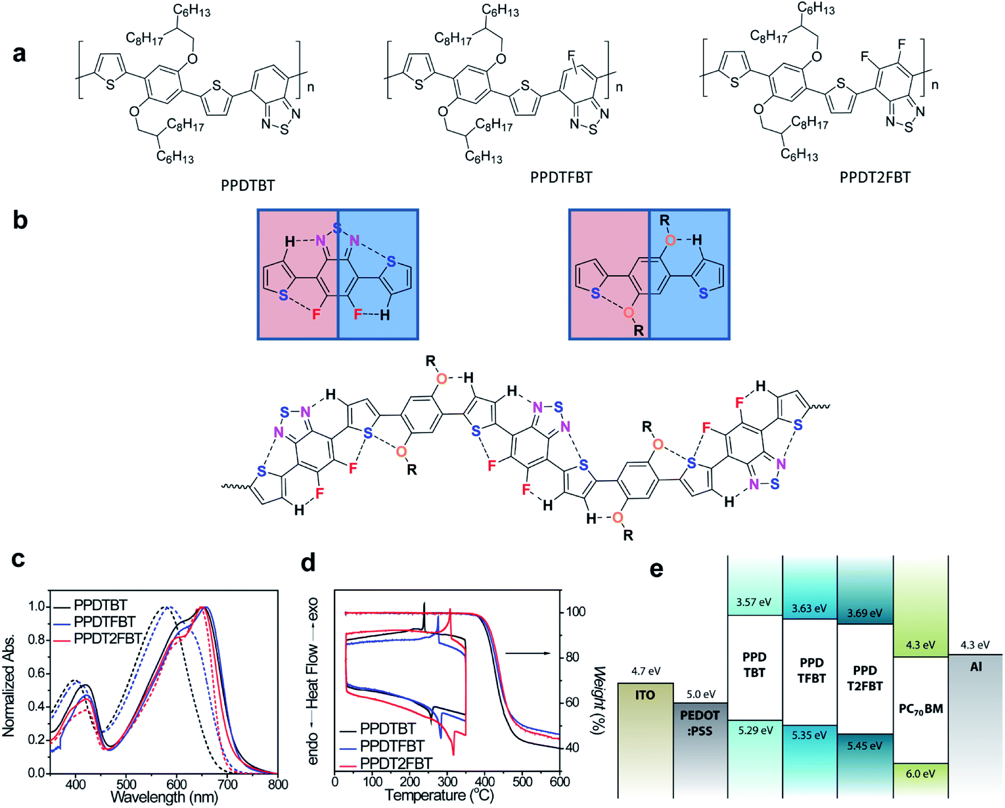
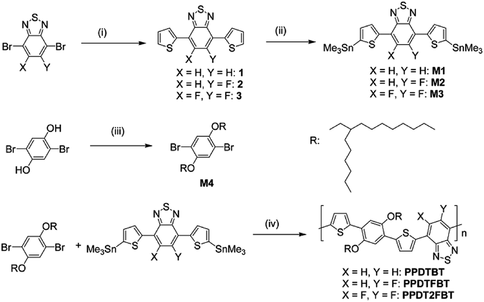
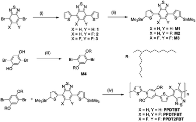
The dialkoxylphenylene and benzothiadiazole (BT)-based monomers were prepared according to the procedures reported in the literature.22–24 1,4-Dibromo-2,5-bis(2-hexyldecyloxy)benzene was reacted with three BT-based monomers, 4,7-bis(5-trimethylstannylthiophen-2-yl)-2,1,3-benzothiadiazole (M1), 4,7-bis(5-trimethylstannyl-thiophen-2-yl)-5-fluoro-2,1,3-benzothiadiazole (M2) and 4,7-bis(5-trimethylstannylthiophen-2-yl)-5,6-difluoro-2,1,3-benzothiadiazole (M3), to yield poly[(2,5-bis(2-hexyldecyloxy)phenylene)-alt-(4,7-di(thiophen-2-yl)benzo[c][1,2,5]thiadiazole)] (PPDTBT), poly[(2,5-bis(2-hexyldecyloxy)phenylene)-alt-(5-fluoro-4,7-di(thiophen-2-yl)benzo[c][1,2,5]thiadiazole)] (PPDTFBT) and poly[(2,5-bis(2-hexyldecyloxy)phenylene)-alt-(5,6-difluoro-4,7-di(thiophen-2-yl)benzo[c][1,2,5]thiadiazole)] (PPDT2FBT), respectively, via Stille cross-coupling with Pd2(dba)3 as a catalyst in chlorobenzene using a microwave reactor (65–70% yield). The chemical structures and synthetic scheme for three polymers are shown in Fig. 1a and Scheme 1, respectively. The detailed synthetic procedures for the monomers are described in the ESI.†22,23 The number-average molecular weight and molecular weight distribution were measured to be 17.8 (polydispersity index, PDI = 2.4), 29.8 (2.4) and 42.6 kDa (2.8) for PPDTBT, PPDTFBT, PPDT2FBT, respectively (Table 1).
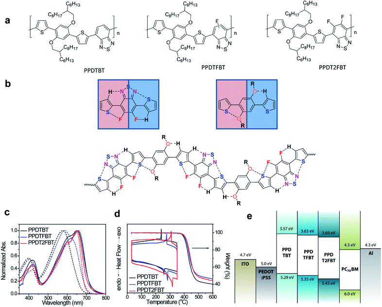 |
| | Fig. 1 (a) Chemical structures, (b) noncovalent attractive interactions within the polymer chain, (c) UV-vis absorption spectra (dashed: in chloroform, solid: in the film), (d) TGA and DSC thermograms of PPDTBT, PPDTFBT and PPDT2FBT and (e) energy-band diagram. | |
 |
| | Scheme 1 Synthetic routes to the monomers and polymers. Reagents and reaction conditions: (i) 2-tributylstannylthiophene, Pd2(dba)3, tris(o-tolyl)phosphine, toluene; (ii) (CH3)3SnCl, LiN(Pr-i)2, THF; (iii) C16H33Br, KOH, 50% TBAB, toluene; (iv) Pd2(dba)3, tris(o-tolyl)phosphine, chlorobenzene. | |
Table 1 Summary of photophysical-, electrochemical- and thermal properties of polymers
| Polymers |
M
n
[kDa] |
PDI |
λ
onset (film) [nm] |
E
optg
[eV] |
HOMOc [eV] |
LUMOd [eV] |
T
d
[°C] |
T
c
[°C] |
T
m
[°C] |
|
Number-average molecular weight (Mn) determined by GPC with o-dichlorobenzene at 80 °C.
Optical band gap in the film.
HOMO level was estimated from the tangential onset of oxidation (Eonsetox) by cyclic voltammetry. HOMO (eV) = −(Eonsetox − Eonsetferrocene + 4.8).
LUMO level was estimated from the HOMO value and optical band gap of the film.
Decomposition temperature (Td) was determined by TGA (with 5% weight-loss).
Crystallization (Tc) and melting (Tm) temperatures were obtained from the peak maxima by DSC.
|
| PPDTBT |
17.8 |
2.4 |
720 |
1.72 |
−5.29 |
−3.57 |
396 |
239 |
257 |
| PPDTFBT |
29.8 |
2.4 |
720 |
1.72 |
−5.35 |
−3.63 |
397 |
276 |
283 |
| PPDT2FBT |
42.6 |
2.8 |
705 |
1.76 |
−5.45 |
−3.69 |
402 |
308 |
317 |
Three different types of dialkoxyphenylene and BT-based LBG copolymers were designed by carefully considering the planarity, chain curvature25 and the resulting intermolecular orientations. The noncovalent attractive interactions between S (in thiophene) and O (in alkoxy groups), between S (in thiophene) and F, and between C–H (in thiophene) and N (in BT) minimize the torsional angle, thus maximizing the planarity of the polymer chain (Fig. 1b).13–18,26,27 Noncovalent coulomb interactions have been utilized to increase the planarity and ordering of polymer chains. Guo et al. demonstrated the use of noncovalent S⋯O attractive interactions to fix the chain conformation with improved planarity in methoxy-substituted thiophene and bithiazoles (dihedral angle, ∼0°) compared to unsubstituted (∼22°) and methyl-substituted thiophene-containing analogues (∼68°).17 S⋯F interactions have been emphasized in controlling the stacking orientation in fluorinated benzobisbenzothiophenes by single-crystal X-ray analyses.13 Recently, Ratner and coworkers reported the role of nonbonding interactions in determining conformations of conjugated polymers and small molecules.28 In this paper, the binding energy was calculated to be 2.2, 0.51 and 0.44 kcal mol−1 for CH⋯N, O⋯S and F⋯S nonbonding interactions, respectively. The branched 2-hexyldecyloxy substituents endow great solubility in common organic solvents with little influence on the intermolecular packing in the film by keeping the branching point away from the main chain. Additionally, by changing the number of fluorine substituents, the electronic structures (such as frontier orbital energy levels) of the polymers can be fine-tuned, which significantly influences the thermal, electrical properties and temporal stabilities of the resulting devices.
Computational studies using density functional theory (DFT, Jaguar quantum chemistry software, M06-2X/6-31G** level) were performed.29-33 As shown in Fig. S1†, torsional profiles obtained by the introduction of fluorine atoms (in PPDTFBT and PPDT2FBT) were expected to be similar with that of PPDTBT because of the small size of fluorine atoms and intrachain F⋯S interactions. The introduction of alkoxy substituents on the phenylene ring was observed to decrease the torsional angle (18.4°–20.9°) via the S⋯O noncovalent interaction compared to the alkyl-substituted structure (38.6°). Fig. S1† shows the minimum energy conformations of PPDTBT, PPDTFBT and PPDT2FBT. According to the torsional profiles for PPDT2FBT, there are two minimum energy conformations for the thiophene–dialkoxybenzene linkage. This means that the S⋯O interaction is comparable with that of the O⋯H–C interaction (Fig. S1(b)†). The same argument can be applied to the thiophene–difluoro BT linkage (Fig. S1(a)†). We guess that these minimum energy conformations are expected to repeat randomly in the polymeric backbone for the polymers, as displayed in Fig. 1b. In order to estimate interchain packing interactions, the binding energies were calculated by considering three types of cofacial interactions.34 The head-to-tail (HT) configuration was found to be the most stable among the various possible configurations for all the polymers (Fig. S2†). The calculated binding energies of HT-type cofacial dimers were −18.7, −22.5, and −24.2 kcal mol−1 for PPDTBT, PPDTFBT and PPDT2FBT, respectively. In particular, the introduction of fluorine substituents greatly affected the interchain packing by way of attractive C–F⋯H, F⋯S and C–F⋯πF interactions in the adjacent polymeric chains.35,36 As shown in Fig. S2,† the replacement of methoxy substituents on the phenylene ring with ethyl groups destabilized the structure by ∼3 kcal mol−1 because of the twisting in the main chain caused by the absence of S⋯O or O⋯H–C interactions. The HOMO levels were measured to be −5.29, −5.35 and −5.45 eV for PPDTBT, PPDTFBT and PPDT2FBT by cyclic voltammetry (CV) (Fig. S3†), respectively. The LUMO levels were estimated to be −3.57, −3.63 and −3.69 eV for PPDTBT, PPDTFBT and PPDT2FBT, respectively, from the HOMO values and the optical band gaps of the films. Though the HOMO and LUMO electronic structures were calculated to be similar for the three polymers (Fig. S4†), their energies were clearly stabilized upon fluorine substitution. The resulting energy band structures are also summarized in Fig. 1e.
Fig. 1c shows the normalized UV-vis absorption spectra of the polymers in chloroform and in the film. All the polymers exhibit broad absorption in the range of 350–750 nm with two distinct high and low energy bands attributed to the localized π–π* and internal charge transfer transitions, respectively. In chloroform, the maximum absorption was measured at λabs = ∼575 nm, ∼585 nm and ∼650 nm for PPDTBT, PPDTFBT and PPDT2FBT, respectively. More importantly, the shoulder peak at 650 nm was gradually enhanced with increasing fluorine substitution. In the film, three polymers show similar UV-vis profiles, where the spectra are red-shifted and the shoulder peak is substantially intensified, relative to those in solution. The differences in UV-vis spectra in the solution and film emphasize the facile interchain organization in the solid state. Optical band gaps were determined to be 1.72–1.76 eV for the polymer films. Thermal stability of the polymers was analyzed by thermogravimetric analysis (TGA) and differential scanning calorimetry (DSC) (Fig. 1d). PPDTBT, PPDTFBT and PPDT2FBT showed the decomposition onset temperatures with 5% weight loss at 396, 397 and 402 °C, respectively. Clear melting temperatures (Tm) at 257, 283 and 317 °C, and recrystallization points (Tc) at 239, 276 and 308 °C were measured for PPDTBT, PPDTFBT and PPDT2FBT, respectively, indicating clear crystalline nature of the polymers. This clearly indicates that the introduction of fluorine atoms has a significant effect on the thermal properties of the polymers. Detailed optical, electrochemical and thermal properties of the three polymers are summarized in Table 1.
2.2. Photovoltaic device characterization
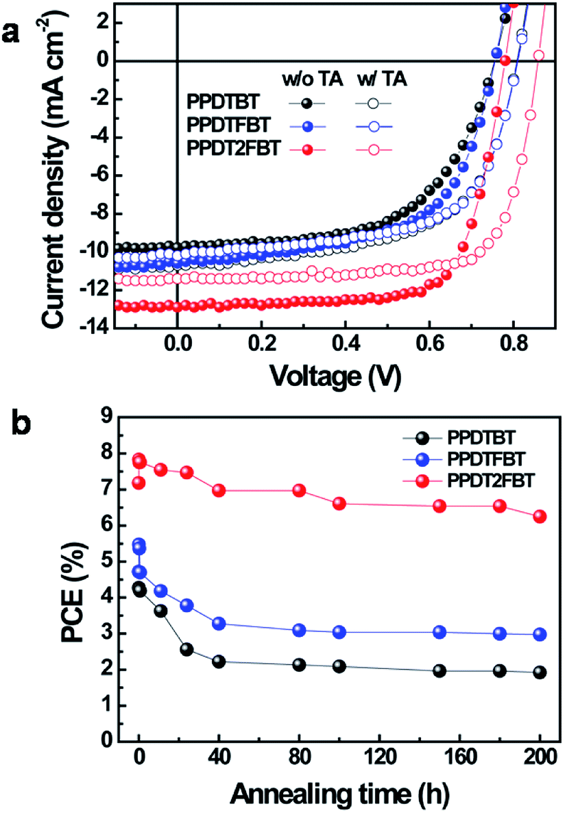
We investigated the photovoltaic properties of the polymers with a simple device architecture of ITO/PEDOT:PSS/polymer:PC70BM/Al (PEDOT:PSS, poly(3,4-ethylenedioxythiophene):polystyrene sulfonic acid; PC70BM, [6,6]-phenyl-C71 butyric acid methylester). To optimize the donor and acceptor (D![[thin space (1/6-em)]](https://www.rsc.org/images/entities/char_2009.gif) :A) blend ratio, polymer:PC70BM blend films were processed using o-dichloro-benzene (DCB) as a solvent (Fig. S5 and Table S1†). For all polymers, devices with a D:A weight ratio of 1:1.5 showed the best performance (PCE: 4.27%, 4.72% and 7.18% for PPDTBT, PPDTFBT and PPDT2FBT, respectively). The device using PPDT2FBT exhibited the highest PCE of 7.18% with a JSC of 12.9 mA cm−2, VOC of 0.78 V and FF of 0.71. This is one of the highest PCE values reported so far for conventional PSCs without any post-treatments (i.e., thermal, solvent annealing and additives, etc.). Upon thermal annealing (130 °C for 10 min), VOC and FF were substantially improved for the three polymer systems (Fig. 2a and Table 2). The VOC increased from 0.76–0.78 V to 0.81–0.86 V and the FF improved by ∼0.03. This must be due to morphological changes in the photoactive layer and improved contact between the active layer and the electrode. Similar results have been reported.37 Temporal stabilities of the devices were also characterized by annealing at 130 °C for 200 h under nitrogen (Fig. 2b). After thermal annealing for 200 h, the PPDTBT device showed a ∼55% decrease in PCE. Interestingly, the PSCs based on PPDTFBT and PPDT2FBT showed a substantial improvement in temporal stability, showing 37% and 13% reductions in PCE, respectively. This remarkable device stability must be closely related to the stronger intermolecular interaction and higher interchain ordering, which is also consistent with the TGA and DSC measurements. Furthermore, relatively small morphological changes were detected for the PPDT2FBT:PC70BM blend film after thermal annealing, compared to those of other two polymers and P3HT blends by atomic force microscopy (AFM) (Fig. 3). Until now, there have been few reports on conjugated polymers achieving both high efficiency of over 7% and long-term thermal stability for over 200 h in PSCs (Table S2 and S2-1†).
:A) blend ratio, polymer:PC70BM blend films were processed using o-dichloro-benzene (DCB) as a solvent (Fig. S5 and Table S1†). For all polymers, devices with a D:A weight ratio of 1:1.5 showed the best performance (PCE: 4.27%, 4.72% and 7.18% for PPDTBT, PPDTFBT and PPDT2FBT, respectively). The device using PPDT2FBT exhibited the highest PCE of 7.18% with a JSC of 12.9 mA cm−2, VOC of 0.78 V and FF of 0.71. This is one of the highest PCE values reported so far for conventional PSCs without any post-treatments (i.e., thermal, solvent annealing and additives, etc.). Upon thermal annealing (130 °C for 10 min), VOC and FF were substantially improved for the three polymer systems (Fig. 2a and Table 2). The VOC increased from 0.76–0.78 V to 0.81–0.86 V and the FF improved by ∼0.03. This must be due to morphological changes in the photoactive layer and improved contact between the active layer and the electrode. Similar results have been reported.37 Temporal stabilities of the devices were also characterized by annealing at 130 °C for 200 h under nitrogen (Fig. 2b). After thermal annealing for 200 h, the PPDTBT device showed a ∼55% decrease in PCE. Interestingly, the PSCs based on PPDTFBT and PPDT2FBT showed a substantial improvement in temporal stability, showing 37% and 13% reductions in PCE, respectively. This remarkable device stability must be closely related to the stronger intermolecular interaction and higher interchain ordering, which is also consistent with the TGA and DSC measurements. Furthermore, relatively small morphological changes were detected for the PPDT2FBT:PC70BM blend film after thermal annealing, compared to those of other two polymers and P3HT blends by atomic force microscopy (AFM) (Fig. 3). Until now, there have been few reports on conjugated polymers achieving both high efficiency of over 7% and long-term thermal stability for over 200 h in PSCs (Table S2 and S2-1†).
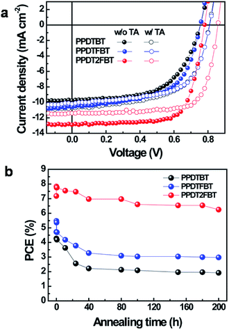 |
| | Fig. 2 (a) Current density versus voltage (J–V) characteristics (w/o TA: without thermal annealing, w/TA: with thermal annealing) and (b) temporal stability (at an annealing temperature of 130 °C) of polymer:PC70BM PSCs. All devices were prepared from o-dichlorobenzene solutions. | |
Table 2 Device characteristics of polymer:PC70BM-based PSCs with thermal annealing (solvent: DCB, blend ratio: 1:1.5)
| Polymer |
Thermal annealinga |
J
SC (mA cm−2) |
V
OC (V) |
FF |
PCE (%) Best/Ave. |
|
Thermal annealing at 130 °C for 10 min.
|
| PPDTBT |
No |
9.77 |
0.76 |
0.58 |
4.27/4.12 |
| Yes |
10.40 |
0.81 |
0.61 |
5.08/4.89 |
| PPDTFBT |
No |
10.6 |
0.76 |
0.59 |
4.72/4.38 |
| Yes |
10.2 |
0.81 |
0.62 |
5.11/5.02 |
| PPDT2FBT |
No |
12.9 |
0.78 |
0.71 |
7.18/6.94 |
| Yes |
11.40 |
0.86 |
0.74 |
7.26/7.06 |
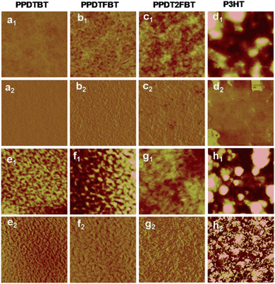 |
| | Fig. 3 Tapping-mode AFM topography and phase images of polymer:PC70BM blend films (solvent: DCB) before and after thermal treatment at 130 °C for 200 h. Before thermal treatment: PPDTBT (a1 and a2), PPDTFBT (b1 and b2), PPDT2FBT (c1 and c2), P3HT (d1 and d2). After thermal treatment: PPDTBT (e1 and e2), PPDTFBT (f1 and f2), PPDT2FBT (g1 and g2), P3HT (h1 and h2). The size of all images is 1.5 μm × 1.5 μm. | |
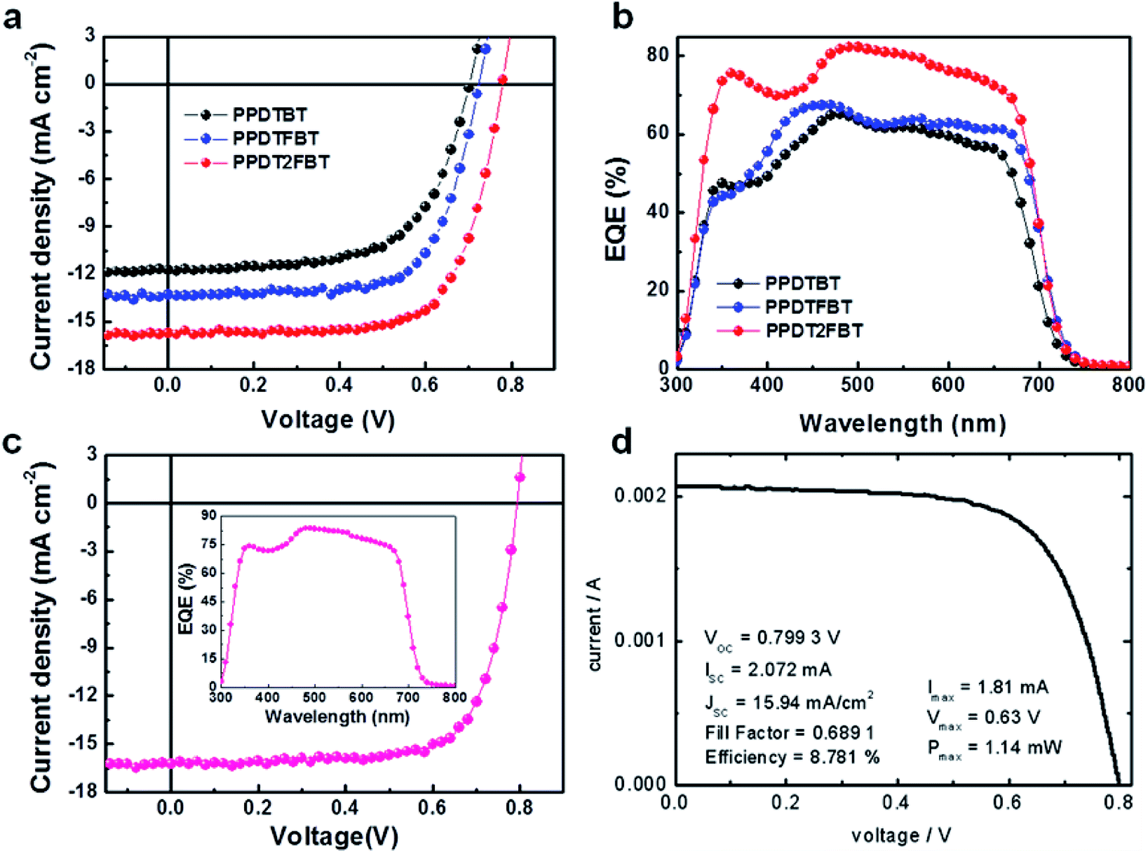
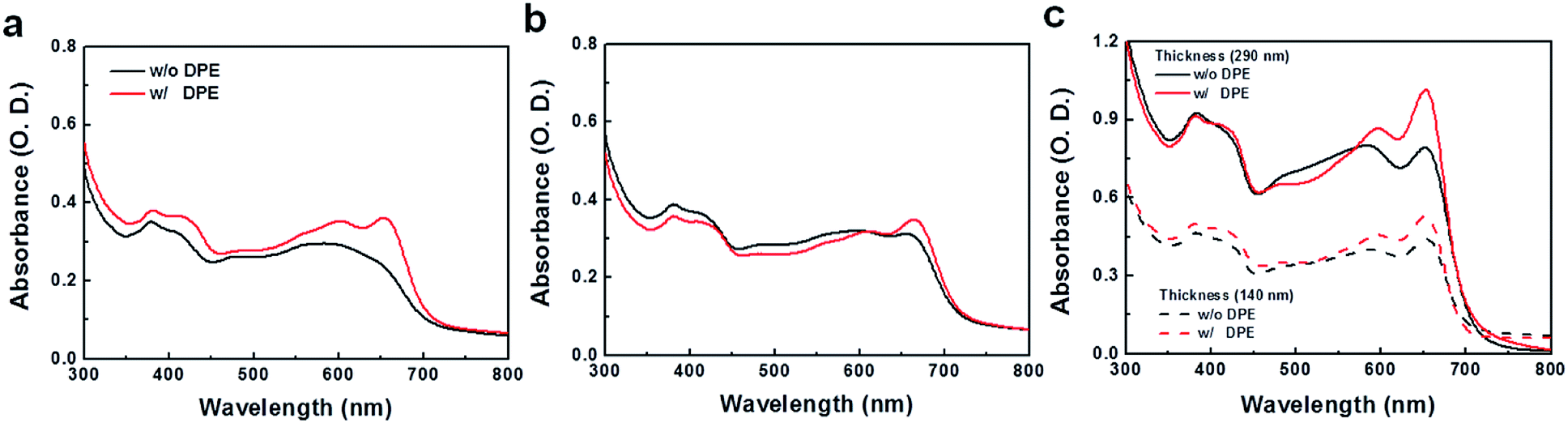
Processing additives offer an efficient way to control the morphology of the active layer by selectively solvating one of the components in BHJ systems.38–40 Several additives were tested to modulate the morphology of the blend films prepared from a 1 wt% chlorobenzene (CB) solution, where the clearer additive effects were observed compared to the films from DCB solutions. In contrast to poor performances of the devices fabricated without processing additives (Fig. S6 and Table S3†), devices with additives showed substantial improvements in photovoltaic properties. Among the tested additives, diphenyl ether (DPE) was found to be an appropriate processing additive for our polymers. The addition of DPE to CB (CB:DPE = 98:2 by volume) led to remarkable enhancements in device performances for the three polymeric structures, showing ca. 5–8% PCE values (Fig. 4). PPDTBT:PC70BM and PPDTFBT:PC70BM devices showed the best PCE with a film thickness of ∼170 nm. Interestingly, the PPDT2FBT blend film exhibited the best efficiency using a thick (290 nm) film (as shown in Fig. S7 and Table S4†). Fig. 4a and b show the J–V characteristics and external quantum efficiency (EQE) of the devices with DPE. Table 3 summarizes the detailed photovoltaic parameters. The PPDT2FBT device showed the highest PCE of 8.64% with a JSC of 15.73 mA cm−2, VOC of 0.78 V and FF of 0.71, reaching EQE values of over 80% in the range of 470–550 nm with a maximum EQE of 82.5% at 490 nm (Fig. 4b). These enhancements in JSC and FF by the addition of DPE are closely related to the strong interchain ordering with the recovery of the strong shoulder peak (originating from strong intermolecular packing and/or π–π stacking) of polymer:PC70BM blend films in UV-vis spectra (Fig. 5). In addition, we also measured a remarkable temporal stability of PPDTFBT- and PPDT2FBT-blend films (in CB without DPE) at 130 °C for 200 h, compared to PPDTBT and P3HT based devices (Fig. S8a†). For devices with the processing additive (DPE), poor thermal stability was measured, showing a gradual decrease in PCE, compared to the devices without DPE (Fig. S8b†). It has been recognized previously that thermal treatment induces agglomeration with a concomitant decrease in device performance with processing additives. The solvent additive allows the components to remain partially dissolved, thus affecting the morphology and diffusion rate of fullerene molecules in the polymer matrix, and promoting the growth of fullerene agglomerates. This can accelerate phase separation between the polymer and fullerene moieties during heat treatment, adversely affecting device performance.41
 |
| | Fig. 4 Photovoltaic characteristics of polymer:PC70BM-based devices fabricated using a CB:DPE solvent mixture. (a) Current density versus voltage (J–V) characteristics and (b) external quantum efficiency (EQE) of polymer:PC70BM-based PSCs. (c) J–V characteristics of the optimized PPDT2FBT:PC70BM-based PSC obtained from our laboratory and (d) certified by the KIER, respectively (c and d: with MeOH treatment). The inset of Fig. 4c shows the EQE values over 80% in the range of 460–570 nm with the maximum EQE of 83.6% at 490 nm. | |
Table 3 Summary of photovoltaic characteristics (prepared from a solvent mixture of CB and DPE)
| Polymer |
Active layer thickness (nm) |
MeOH treatment |
J
SC (mA cm−2) |
V
OC (V) |
FF |
J
SC [cal.]a (mA cm−2) |
PCE (%) |
| Best |
Ave. |
|
J
SC [cal.], calculated JSC from a EQE curve.
|
| PPDTBT |
170 |
No |
11.73 |
0.70 |
0.63 |
11.77 |
5.17 |
5.04 |
| PPDTFBT |
175 |
13.29 |
0.73 |
0.69 |
12.88 |
6.64 |
6.45 |
| PPDT2FBT |
290 |
15.73 |
0.78 |
0.71 |
15.59 |
8.64 |
8.39 |
| PPDT2FBT |
290 |
Yes |
16.30 |
0.79 |
0.73 |
15.94 |
9.39 |
9.21 |
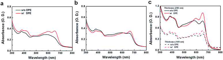 |
| | Fig. 5 UV-vis absorption spectra of polymer:PC70BM blend films based on (a) PPDTBT, (b) PPDTFBT and (c) PPDT2FBT. The films were prepared with CB (w/o DPE) and mixed CB:DPE (98:2 vol%, w/DPE) as a solvent. | |
To further optimize the PPDT2FBT device, the top of the active layer was treated with methanol (MeOH). Solvent treatments can be an effective strategy for simultaneously enhancing all device parameters.42,43Fig. 4c and d show J–V characteristics of optimized, MeOH treated, PPDT2FBT:PC70BM devices as measured in our laboratory and certified by the Korea Institute of Energy Research (KIER), respectively. More than 50 devices were fabricated for device optimization. The best performing device exhibited a PCE of 9.39% (average PCE = 9.21%) with a JSC of 16.30 mA cm−2, VOC of 0.79 V and FF of 0.73 (Table 3). The EQE values of these devices are above 80% in the range of 460–570 nm with a maximum EQE of 83.6% at 490 nm (inset of Fig. 4c). The surface morphologies of PPDT2FBT:PC70BM films with and without MeOH treatments were characterized by AFM (Fig. S9†). There were no observable changes in the AFM images, indicating that the effects of MeOH treatment do not arise from reconstruction of the film surface. Similar data and the detailed studies on the MeOH treatment effects have been reported previously. Bazan and Heeger et al. reported that MeOH treatment enhanced the photovoltaic efficiency by increasing the internal electric field and surface potential by Kelvin probe force microscopy (KPFM) and impedance measurements. Additionally, the series resistance decreased and the shunt resistance increased after methanol treatment, in good agreement with the observed improvements in JSC and FF.42,43 A certified PCE of 8.78% was obtained by the KIER (Fig. 4d and S10†) from a UV-epoxy encapsulated sample. This PCE was ∼5% lower than the average PCE as measured in our laboratory, which could be attributed to non-ideal encapsulation.7,44 The certified results confirm that the measured PCE values of over 9%, as obtained in our laboratory, are reasonable. Furthermore, this work is the first report that showcases efficiency over 9% with a conventional-type, 290 nm thick, single cell structure without any additional interfacial layer (Table S5†). The high PCE and device thickness also suggest a meaningful approach for real commercial applications of PSCs. Although remarkable improvements in PCE have been reported in PSCs, the device thickness is on the order of ∼100 nm. It is of great importance to develop photovoltaic materials which can function effectively at the greater film thickness. It is not currently viable to fabricate uniform and defect-free films on the order of 100 nm thickness using industrial solution casting techniques. Most previous PSCs showed that the performance degrades with the concomitant decrease in FF, with increasing film thickness. This must be closely related to space charge accumulation and charge recombination losses which become stronger with thicker films. It is noteworthy to emphasize that a ∼300 nm thick active layer in the PPDT2FBT:PC70BM device attenuates incident light almost completely without damage in the fill factor (0.71–0.73), showing a high JSC of 15.7–16.3 mA cm−2. These superior properties are closely related to the molecular structures and pronounced crystalline morphology in the film.
2.3. Morphological and charge transport characteristics
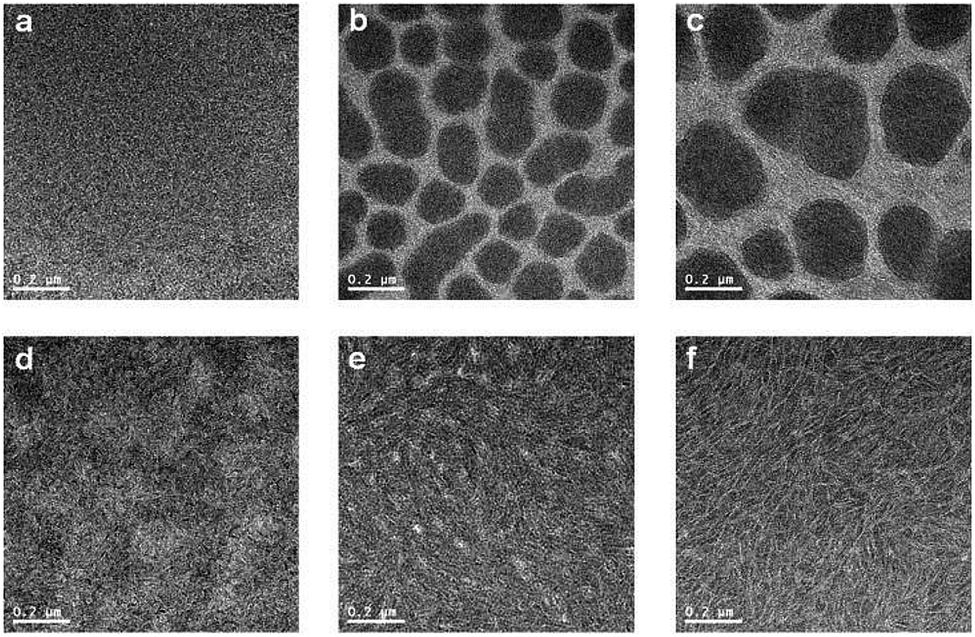
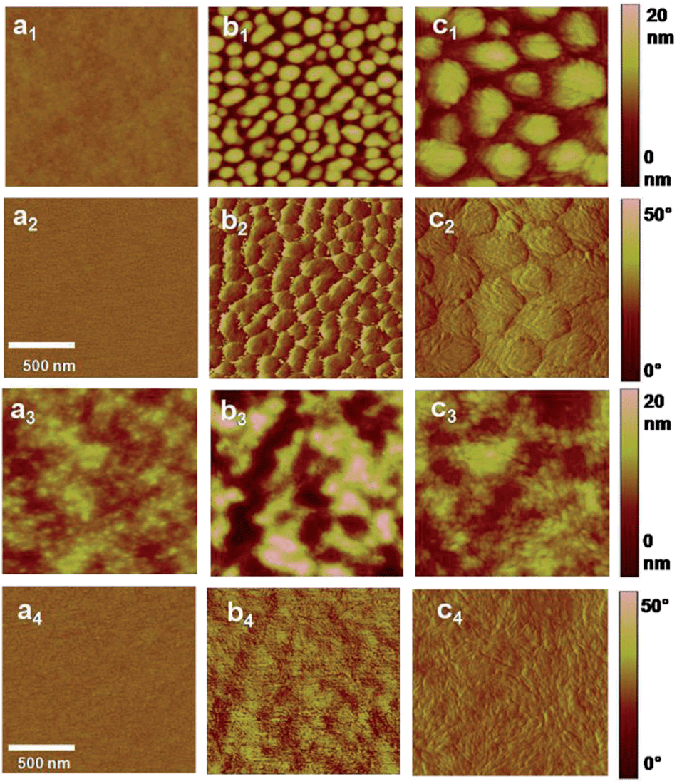
The nanoscale morphology of polymer:PC70BM blend films (in CB) was studied by high-resolution transmission electron microscopy (HR-TEM) and tapping mode AFM. In Fig. 6, TEM images show large domains with diameters of 100–300 nm for the PPDTFBT and PPDT2FBT blend films fabricated without DPE, whereas the PPDTBT films show featureless morphologies. Macrophase separation in the PPDTFBT and PPDT2FBT blend films limits the probability for exciton dissociation by reducing donor/acceptor interfacial areas, leading to poor JSC and FF values by charge recombination loss.9,45 In contrast, the blend films with DPE show a clear morphological change for all polymers, forming well-distributed nano-fibrillar structures where a bicontinuous interpenetrating network may be formed in BHJ films with PC70BM. These fibrillar structures are expected to enhance the charge-carrier mobility, JSC, FF and the resulting photovoltaic performance of PSCs.44,46 Surface topography and phase images of the three blend films obtained from AFM measurements are consistent with morphologies observed in HR-TEM images (Fig. 7).
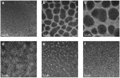 |
| | Fig. 6 HR-TEM images of polymer:PC70BM films without (a–c) and with DPE (d–f). PPDTBT (a and d), PPDTFBT (b and e) and PPDT2FBT (c and f). | |
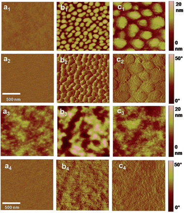 |
| | Fig. 7 Tapping-mode AFM topography (a1–c1, a3–c3) and phase (a2–c2, a4–c4) images of polymer:PC70BM blend films. Without DPE: PPDTBT (a1 and a2), PPDTFBT (b1 and b2) and PPDT2FBT (c1 and c2). With DPE: PPDTBT (a3 and a4), PPDTFBT (b3 and b4) and PPDT2FBT (c3 and c4). The size of all images is 1.5 μm × 1.5 μm. | |
In order to quantify charge carrier mobilities, hole-only (ITO/PEDOT:PSS/polymer:PC70BM/Au) and electron-only (FTO/polymer:PC70BM/Al, FTO: fluorine-doped tin oxide) diodes were prepared47 using optimized BHJ films (CB:DPE = 98:2 vol%) with various film thicknesses (200–1000 nm) and their J–V characteristics were analyzed by the space charge limited current (SCLC, JSCL) method. The potential loss due to the series resistance of the ITO and the built-in potential were carefully considered in order to ensure accuracy in the measurements. The J–V characteristics show a quadratic dependence on voltage over a range of several volts and an inverse cubic dependence on the film thickness, consistent with the Mott–Gurney relationship (eqn (1)),48,49
where
ε0 is the free-space permittivity,
εr is the dielectric constant of the semiconductor,
μ is the mobility,
V is the applied voltage and
L is the thickness of the active layer.
The average hole and electron mobilities were determined to be μ (hole) = 3.2 × 10⁻⁴, 5.5 × 10⁻⁴ and 3.0 × 10⁻³ cm2 V−1 s−1, and μ (electron) = 2.8 × 10⁻⁴, 4.2 × 10⁻⁴ and 1.5 × 10⁻³ cm2 V−1 s−1 for PPDTBT, PPDTFBT and PPDT2FBT devices, respectively. Plots of films with similar thickness are found in Fig. 8, while additional plots with films of various thicknesses are found in Fig. S11 and Table S6.† All the polymers showed well balanced hole/electron mobility ratios in the range of 1–2 with various film thicknesses. PPDT2FBT showed ∼1 order higher hole and electron mobilities relative to other two polymers. Notably, PPDT2FBT showed negligible changes in the carrier mobility even at ∼1 μm film thickness. These SCLC results are consistent with the PCE data of PPDT2FBT, showing no decrease in VOC and FF with a 290 nm thick active layer, resulting in a high JSC of 15.7–16.3 mA cm−2 due to the increased light absorption.
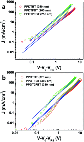 |
| | Fig. 8
J–V characteristics of (a) hole- and (b) electron-only devices based on polymer:PC70BM blend films (solvent: CB:DPE = 98:2 vol%). Blue lines represent fits of the curves using the Mott–Gurney relationship. | |
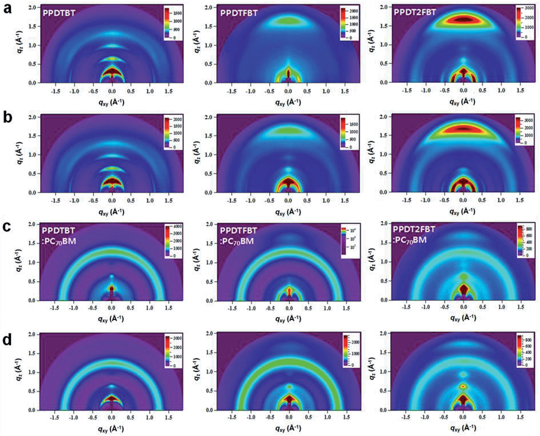
To further understand the detailed film morphology of the three polymers with/without PC70BM and before/after additive treatments, the molecular arrangements and packing characteristics of the thin films were studied by grazing incidence wide angle X-ray scattering (GIWAXS).43,50Fig. 9 shows GIWAXS patterns for pristine polymer and polymer:PC70BM blend films prepared from CB solutions with and without DPE. From the GIWAXS profiles, packing parameters were extracted and are listed in Table S7.† Pronounced reflection peaks of (100), (200), and (300) in the out-of-plane direction were observed in the pristine PPDTBT film, showing a lamellar spacing of 18.9 Å (Fig. 9a and S12†). For the pristine PPDTFBT and PPDT2FBT films, the lamellar spacing calculated from the (100) diffraction peak was slightly increased to 20.7 Å. On increasing the number of fluorine substituents on the BT unit, the in-plane lamellar diffraction peak was also intensified (strongest in PPDT2FBT). Therefore, the presence of fluorine atom may induce a face-on lamellar orientation coexisting with the edge-on lamellar stacks, which may facilitate an effective three-dimensional charge transport. The PPDTBT sample showed no π–π stacking (010) peak in the out-of-plane direction. Interestingly, the (010) peak (d = ∼3.7 Å) in the out-of-plane direction becomes pronounced by the introduction of fluorine substituents. The π–π stacking distance was shorter in PPDT2FBT (3.72 Å) than in PPDTFBT (3.78 Å), which indicates a stronger cofacial interchain orientation between the neighboring chains. Upon addition of DPE to the pristine polymer films, similar trends were observed with increased scattering intensity, indicating more pronounced interchain orientation with DPE. The GIWAXS patterns of polymer:PC70BM blend films are shown in Fig. 9c and d. The lamellar spacing for polymer:PC70BM blend samples was measured to be 19.1–19.9 Å for the three structures, showing similar spacings in the pristine polymer films. Upon addition of DPE, the diffraction patterns are clearer without noticeable changes in the lamellar spacing. We also observed a further reduction in the π–π stacking distance (3.57–3.59 Å) for the PPDTFBT:PC70BM and PPDT2FBT:PC70BM films with DPE, indicating an intensified interchain orientation upon addition of DPE. Interestingly, the blend films with DPE show shorter π–π stacking distances than those of the pristine polymers (PPDTFBT: 3.78 Å and PPDT2FBT: 3.72 Å). The solvent additive allows the components to remain partially dissolved and affects the morphology and diffusive rate of PC70BM in the polymer matrix. This may allow a longer time for polymer chains to self-organize into highly ordered intermolecular structures.51
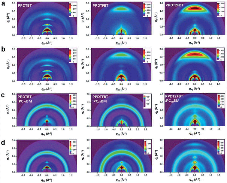 |
| | Fig. 9 Grazing incidence wide angle X-ray scattering (GIWAXS) images. GIWAXS images of pristine polymer films (upper two rows) (a) without and (b) with DPE, and polymer:PC70BM blend films (lower two rows) (c) without and (d) with DPE. Left, middle and right panels show the images for PPDTBT, PPDTFBT and PPDT2FBT, respectively. | |
3. Conclusion
In summary, a series of dialkoxyphenylene-BT containing semi-crystalline LBG polymers were synthesized with noncovalent conformational locking to enhance chain planarity, intermolecular ordering and thermal stability without losing solution processability. The polymers formed well-distributed interpenetrating nano-fibrillar networked morphologies with PC70BM, showing well-balanced hole and electron mobilities. Notably, PSCs based on these polymers exhibited PCEs of up to 9.39% in a 290 nm thick conventional single-cell device structure without any additional interfacial layer. The thick active layer (290 nm) in the PPDT2FBT:PC70BM device enabled strong light absorption, yielding a high JSC of 15.7–16.3 mA cm−2 without the loss in VOC and FF. It is of great importance to develop photovoltaic materials which can function effectively at the thicker film which can absorb solar light completely and is viable to be produced using industrial solution processing techniques. These remarkable device characteristics with the great thickness are closely related to the highly ordered organization of polymer chains via noncovalent attractive interactions, showing nano-fibrillar structures in TEM with tight interchain packing (a π–π stacking distance of 3.57–3.59 Å) in the blend films. In addition, we also measured clear molecular weight dependence on the photovoltaic properties. We synthesized more than 20 batches of PPDT2FBT to optimize the photovoltaic characteristics. Among them, the high molecular weight batches (with ∼40 kDa) showed the PCE over 8–9% but small molecular weight batches showed the relatively lower PCE values (∼7%). The detailed study on the molecular weight dependence is now under investigation. Furthermore, this work also demonstrates a high PCE of over 7% (without any post-treatments) with long-term thermal stability at 130 °C for ∼200 h. These new polymers provide a great possibility to overcome the efficiency barrier of 10% and accelerate the real application of plastic solar cells.
4. Experimental section
4.1. General
A microwave reactor (Biotage Initiator™) was used to synthesize the polymers. 1H and 13C NMR spectra were recorded on a JEOL (JNM-AL300) FT NMR system operating at 300 MHz and 75 MHz, respectively. UV-vis spectra were obtained with a JASCO V-630 spectrophotometer. The number- and weight-average molecular weights of the polymers were determined by gel-permeation chromatography (GPC) with o-dichlorobenzene as an eluent at 80 °C on an Agilent GPC 1200 series, relative to polystyrene standards. Cyclic voltammetry (CV) experiments were performed with a Versa STAT 3 analyzer. All CV measurements were carried out in 0.1 M tetrabutylammoniumtetrafluoroborate (Bu4NBF4) in acetonitrile with a conventional three-electrode configuration employing a platinum wire as a counter electrode, platinum electrode coated with a thin polymer film as a working electrode, and Ag/Ag+ electrode as a reference electrode (scan rate: 50 mV s−1). Thermogravimetric analysis (2050 TGA V5.4A) and differential scanning calorimetry (DSC Q200 V24.4) measurements were performed at a heating and cooling rate of 10 °C min−1 under nitrogen (purity, 99.999%). The nanoscale morphology of the polymer films was investigated using high-resolution transmission electron microscopy (HR-TEM) (JEM-2100, Cs corrector). Atomic force microscopy (AFM) images (1.5 μm × 1.5 μm) were obtained using a Veeco AFM microscope in tapping mode. Carrier mobilities were calculated by the space charge limited current method using hole-only (ITO/PEDOT:PSS/active layer/Au) and electron-only (FTO/active layer/Al, FTO: fluorine-doped tin oxide) diodes by fitting their J–V characteristics with the Mott–Gurney equation (eqn (1)).37,38 Corrections were made for the built in potential (V0) of the devices due to differences in the work functions of the electrodes and for the loss in potential due to the series resistance (VRS) using the equation VRS = I × RS. The thickness (L) of each device was measured after collecting J–V data using an atomic force microscope and a value of 3 was assumed for εr.
4.2. Synthesis of polymers
In a glove box, M1 (0.230 g, 0.32 mmol), M4 (0.263 g, 0.32 mmol), tris(dibenzylideneacetone)dipalladium(0) (4 mol%), tri(o-tolyl)phosphine (8 mol%) and 1 mL chlorobenzene were added in a 5 mL microwave vial. The polymerization reaction mixture was heated at 80 °C (65 W, 10 min), at 100 °C (70 W, 10 min) and at 140 °C (80 W, 40 min) in a microwave reactor. The polymer was end-capped by addition of 2-tributylstannylthiophene (0.05 g, 0.14 mmol) and the mixture was further reacted at 140 °C for 20 min. The solution was cooled down and 2-bromothiophene (0.09 g, 0.53 mmol) was added by a syringe. The reaction solution was heated at 140 °C for another 20 min. After the reaction was finished, the crude PPDTBT polymer was precipitated into the mixture of methanol and HCl (36%) (350 mL:10 mL) and further purified by Soxhlet extraction with acetone, hexane and chloroform. The extracted PPDTBT polymer in chloroform was precipitated into MeOH, filtered and dried under vacuum. PPDTFBT and PPDT2FBT were synthesized by following the same procedure as PPDTBT.
Poly[(2,5-bis(2-hexyldecyloxy)phenylene)-alt-(4,7-di(thiophen-2-yl)benzo[c][1,2,5]-thiadiazole)] (PPDTBT).
Yield: 70%. Number-average molecular weight (Mn) = 17.8 kDa, polydispersity index (PDI) = 2.4. δH (300 MHz; CDCl3) 0.86–2.02 (62H, br), 4.10 (4H, br), 7.48 (2H, br), 7.69 (2H, br), 7.91 (2H, br), 8.19 (2H, br).
Poly[(2,5-bis(2-hexyldecyloxy)phenylene)-alt-(5-fluoro-4,7-di(thiophen-2-yl)benzo[c][1,2,5]-thiadiazole)] (PPDTFBT).
Yield: 65%. Mn = 29.8 kDa, PDI = 2.4. δH (300 MHz; CDCl3) 0.86–2.02 (62H, br), 4.06 (4H, br), 7.06–8.20 (7H, br).
Poly[(2,5-bis(2-hexyldecyloxy)phenylene)-alt-(5,6-difluoro-4,7-di(thiophen-2-yl)benzo[c][1,2,5]-thiadiazole)] (PPDT2FBT).
Yield: 67%. Mn = 42.6 kDa, PDI = 2.8. δH (300 MHz; CDCl3) 0.86–2.02 (62H, br), 4.00 (4H, br), 7.06–8.20 (6H, br).
4.3. Fabrication and characterization of PSCs
ITO-coated glass substrates were cleaned by ultrasonication in deionized water, acetone and iso-propanol, and then dried in an oven for 12 h. After UV-ozone treatments for 10 min, PEDOT:PSS solution (Baytron P VPAI 4083, H. C. Starck) was spin-coated onto the ITO substrate at 5000 rpm for 40 s and then baked at 140 °C for 10 min. For deposition of the active layer, blend solutions of polymer (1 wt%):PC70BM (1.5 wt%) dissolved in DCB or in CB (with/without 2 vol% diphenyl ether) were spin-cast on top of the PEDOT:PSS layer in a nitrogen-filled glove box. For methanol (MeOH) treatment, MeOH was spin-cast at 1000 rpm for 40 s on top of the active layer. Subsequently, an Al (100 nm) electrode was deposited on top of the active layer under vacuum (<10−6 Torr) by thermal evaporation. The area of the Al electrode defines the active area of the device as 13.0 mm2. For the characterization of PSCs, their current density–voltage (J–V) characteristics were measured using a Keithley 2635A Source Measure Unit. Solar cell performance was tested with an Air Mass 1.5 Global (AM 1.5 G) solar simulator under an irradiation intensity of 100 mW cm−2. EQE measurements were performed using a PV measurement QE system using monochromatic light from a xenon lamp under ambient conditions. The monochromatic light was chopped at 100 Hz and intensity was calibrated relative to a standard Si photodiode using a lock-in-amplifier. A mask (13.0 mm2) made of thin metal was used for J–V characteristics and EQE measurements.
4.4. GIWAXS measurements
GIWAXS measurements were carried out at the PLS-II 9A U-SAXS beam line of Pohang Accelerator Laboratory. X-ray coming from the in-vacuum undulator (IVU) was monochromated (Ek = 11.24 keV, λ = 1.103 Å) using a Si(111) double crystal monochromator and focused horizontally and vertically at the sample position (450 (H) × 60 (V) μm2 in FWHM) using a K–B-type focusing mirror system. The GIWAXS sample stage was equipped with a 7-axis motorized stage for the fine alignment of the thin sample and the incidence angle of X-rays was adjusted to 0.12–0.14°. GIWAXS patterns were recorded with a 2D CCD detector (Rayonix SX165, USA), and X-ray irradiation time was 0.5–5 s depending on the saturation level of the detector. The diffraction angle was calibrated with a sucrose standard (monoclinic, P21, a = 10.8631 Å, b = 8.7044 Å, c = 7.7624 Å, β = 102.938°) and the sample-to-detector distance was approximately 232 mm. Samples for GIWAXS measurements were prepared by spin-coating polymer or polymer:PC70BM blend solutions on top of the Si substrates. We also checked GIWAXS data on top of the PEDOT:PSS/Si layer. We obtained same morphologies with and without PEDOT:PSS layer on the Si substrate.
Acknowledgements
T. L. Nguyen, H. Choi and S.-J. Ko contributed equally to this work. This work was supported by the National Research Foundation (NRF) of Korea (2012R1A1A2005855, 2012M3A6A7055540, 2013M3C1A3065522, 2009-0093020) and the International Cooperation of the Korea Institute of Energy Technology Evaluation and Planning (KETEP) grant funded by the Korea government Ministry of Knowledge Economy (2012T100100740).
Notes and references
- G. Li, R. Zhu and Y. Yang, Nat. Photonics, 2012, 6, 153–161 CrossRef CAS
 ; S. B. Darling and F. You, RSC Adv., 2013, 3, 17633–17648 RSC .
- L. Huo, S. Zhang, X. Guo, F. Xu, Y. Li and J. Hou, Angew. Chem., Int. Ed., 2011, 50, 9697–9702 CrossRef CAS PubMed .
- T. Y. Chu, J. Lu, S. Beaupre, Y. Zhang, J. R. Pouliot, S. Wakim, J. Zhou, M. Leclerc, Z. Li, J. Ding and Y. Tao, J. Am. Chem. Soc., 2011, 133, 4250–4253 CrossRef CAS PubMed .
- L. Dou, J. You, J. Yang, C. C. Chen, Y. He, S. Murase, T. Moriarty, K. Emery, G. Li and Y. Yang, Nat. Photonics, 2012, 6, 180–185 CrossRef CAS .
- J. K. Kim, K. Lee, N. E. Coates, D. Moses, T. Q. Nguyen, M. Dante and A. J. Heeger, Science., 2007, 317, 222–225 CrossRef CAS PubMed .
- C. Cabanetos, A. E. Labban, J. A. Bartelt, J. D. Douglas, W. R. Mateker, J. M. J. Fréchet, M. D. McGehee and P. M. Beaujuge, J. Am. Chem. Soc., 2013, 135, 4656–4659 CrossRef CAS PubMed .
- Z. He, C. Zhong, S. Su, M. Xu, H. Wu and Y. Cao, Nat. Photonics, 2012, 6, 591–595 Search PubMed .
- H. J. Son, L. Lu, W. Chen, T. Xu, T. Zheng, B. Carsten, J. Strzalka, S. B. Darling, L. X. Chen and L. Yu, Adv. Mater., 2013, 25, 838–843 CrossRef CAS PubMed .
- H.-C. Chen, Y. H. Chen, C.-C. Liu, Y.-C. Chien, S.-W. Chou and P.-T. Chou, Chem. Mater., 2012, 24, 4766–4772 CrossRef CAS .
- B. C. Schroeder, Z. Huang, R. S. Ashraf, J. Smith, P. D'Angelo, S. E. Watkins, T. D. Anthopoulos, J. R. Durrant and I. McCulloch, Adv. Funct. Mater., 2012, 22, 1663–1670 CrossRef CAS .
- Y. Zhang, S.-C. Chien, K.-S. Chen, H.-L. Yip, Y. Sun, J. A. Davies, F. C. Chen and A. K.-Y. Jen, Chem. Commun., 2011, 47, 11026–11028 RSC .
- Z. Li, J. Lu, S.-C. Tse, J. Zhou, X. Du, Y. Tao and J. Ding, J. Mater. Chem., 2011, 21, 3226–3233 RSC .
- Y. Wang, S. R. Parkin, J. Gierschner and M. D. Watson, Org. Lett., 2008, 10, 3307–3310 CrossRef CAS PubMed .
- F. Babudri, G. M. Farinola, F. Naso and R. Ragni, Chem. Commun., 2007, 1003–1022 RSC .
- K. Reichenbacher, H. I. Suss and J. Hulliger, Chem. Soc. Rev., 2005, 34, 22–30 RSC .
- W. Lee, H. Choi, S. Hwang, J. Y. Kim and H. Y. Woo, Chem.–Eur. J., 2012, 18, 2551–2558 CrossRef CAS PubMed .
- X. Guo, J. Quinn, Z. Chen, H. Usta, Y. Zheng, Y. Xia, J. W. Hennek, R. P. Ortiz, T. J. Marks and A. Facchetti, J. Am. Chem. Soc., 2013, 135, 1986–1996 CrossRef CAS PubMed .
- X. Guo, F. S. Kim, S. A. Jenekhe and M. D. Watson, J. Am. Chem. Soc., 2009, 131, 7206–7207 CrossRef CAS PubMed .
- D. Beljonne, G. Pourtois, C. Silva, E. Hennebicq, L. M. Herz, R. H. Friend, G. D. Scholes, S. Setayesh, K. Müllen and J. L. Brédas, Proc. Natl. Acad. Sci. U. S. A., 2002, 99, 10982–10987 CrossRef CAS PubMed .
- J. L. Bredas, G. B. Street, B. Themans and J. M. Andre, J. Chem. Phys., 1985, 83, 1323–1329 CrossRef CAS PubMed .
- R. A. Street, J. E. Northrup and A. Salleo, Phys. Rev. B: Condens. Matter Mater. Phys., 2005, 71, 165202 CrossRef .
- L. Biniek, C. L. Chochos, N. Leclerc, O. Boyron, S. Fall, P. Lévèque and T. Heiser, J. Polym. Sci., Part A: Polym. Chem., 2012, 50, 1861–1868 CrossRef CAS .
- J.-F. Jheng, Y.-Y. Lai, J.-S. Wu, Y.-H. Chao, C.-L. Wang and C.-S. Hsu, Adv. Mater., 2013, 25, 2445–2451 CrossRef CAS PubMed .
- J. E. Carlé, J. W. Andreasen, M. Jørgensen and F. C. Krebs, Sol. Energy Mater. Sol. Cells, 2010, 94, 774–780 CrossRef PubMed .
- W. Lee, G.-H. Kim, S.-J. Ko, S. Yum, S. Hwang, S. Cho, Y.-H. Shin, J. Y. Kim and H. Y. Woo, Macromolecules, 2014, 47, 1604–1612 CrossRef CAS .
- S. Yum, T. An, X. Wang, W. Lee, M. A. Uddin, Y. J. Kim, T. L. Nguyen, S. Xu, S. Hwang, C. Park and H. Y. Woo, Chem. Mater., 2014, 26, 2147–2154 CrossRef CAS .
- S. Yum, T. K. An, X. Wang, M. A. Uddin, T. L. Nguyen, S. Xu, H. Ryu, Y. J. Kim, S. Hwang, C. E. Park and H. Y. Woo, Pure Appl. Chem., 2014 DOI:10.1515/pac-2014-0205 .
- N. E. Jackson, B. M. Savoie, K. L. Kohlstedt, M. O. D. L. Cruz, G. C. Schatz, L. X. Chen and M. A. Ratner, J. Am. Chem. Soc., 2013, 135, 10475–10483 CrossRef CAS PubMed .
- Y. Zhao and D. G. Truhlar, Theor. Chem. Acc., 2008, 120, 215–241 CrossRef CAS .
- Y. Zhao and D. G. Truhlar, Acc. Chem. Res., 2008, 41, 157–167 CrossRef CAS PubMed .
- M. Doemer, I. Tavernelli and U. Rothlisberger, J. Chem. Theory Comput., 2013, 9, 955–964 CrossRef CAS .
- K. B. Bravaya, E. Epifanovsky and A. I. Krylov, J. Phys. Chem. Lett., 2012, 3, 2726–2732 CrossRef CAS .
- M. Walker, A. J. A. Harvey, A. Sen and C. E. H. Dessent, J. Phys. Chem. A, 2013, 117, 12590–12600 CrossRef CAS PubMed .
- H.-Y. Chen, J. Hou, A. E. Hayden, H. Yang, K. N. Houk and Y. Yang, Adv. Mater., 2010, 22, 371–375 CrossRef CAS PubMed .
- A. C. Stuart, J. R. Tumbleston, H. Zhou, W. Li, S. Liu, H. Ade and W. You, J. Am.
Chem. Soc., 2013, 135, 1806–1815 CrossRef CAS PubMed .
- H. Bronstein, J. M. Frost, A. Hadipour, Y. Kim, C. B. Nielsen, R. S. Ashraf, B. P. Rand, S. Watkins and I. McCulloch, Chem. Mater., 2013, 25, 277–285 CrossRef CAS .
- P. Kumar, C. Bilen, K. Feron, X. Zhou, W. J. Belcher and P. C. Dastoor, Appl. Phys. Lett., 2014, 104, 193905 CrossRef CAS PubMed ; G. Griffini, J. D. Douglas, C. Piliego, T. W. Holcombe, S. Turri, J. M. J. Frechet and J. L. Mynar, Adv. Mater., 2011, 23, 1660–1664 CrossRef PubMed .
- J. Peet, N. S. Cho, S. K. Lee and G. C. Bazan, Macromolecules, 2008, 41, 8655–8659 CrossRef CAS .
- C. Piliego, T. W. Holcombe, J. D. Douglas, C. H. Woo, P. M. Beaujuge and J. M. J. Fréchet, J. Am. Chem. Soc., 2010, 132, 7595–7597 CrossRef CAS PubMed .
- J. Peet, J. Y. Kim, N. E. Coates, W. L. Ma, D. Moses, A. J. Heeger and G. C. Bazan, Nat. Mater., 2007, 6, 497–500 CrossRef CAS PubMed ; H.-C. Liao, C.-C. Ho, C.-Y. Chang, M.-H. Jao, S. B. Darling and W.-F. Su, Mater. Today, 2013, 16, 326–336 CrossRef PubMed .
- L. Chang, H. W. A. Lademann, J.-B. Bonekamp, K. Meerholz and A. J. Moulé, Adv. Funct. Mater., 2011, 21, 1779–1787 CrossRef CAS .
- J. H. Seo, A. Gutacker, Y. Sun, H. Wu, F. Huang, Y. Cao, U. Scherf, A. J. Heeger and G. C. Bazan, J. Am. Chem. Soc., 2011, 133, 8416–8419 CrossRef CAS PubMed .
- H. Zhou, Y. Zhang, J. Seifter, S. D. Collins, C. Luo, G. C. Bazan, T.-Q. Nguyen and A. J. Heeger, Adv. Mater., 2013, 25, 1646–1652 CrossRef CAS PubMed .
- H.-Y. Chen, J. Hou, S. Zhang, Y. Liang, G. Yang, Y. Yang, L. Yu, Y. Wu and G. Li, Nat. Photonics, 2009, 3, 649–653 CrossRef CAS .
- Y. Liang, Z. Xu, J. Xia, S.-T. Tsai, Y. Wu, G. Li, C. Ray and L. Yu, Adv. Mater., 2010, 22, E135–E138 CrossRef CAS PubMed .
- X. Yang, J. Loos, S. C. Veenstra, W. J. H. Verhees, M. M. Wienk, J. M. Kroon, M. A. J. Michels and R. A. J. Janssen, Nano Lett., 2005, 5, 579–583 CrossRef CAS PubMed .
- A. R. V. Benvenho, R. Lessmann, I. A. Hummelgen, R. M. Q. Mello, R. W. C. Li, F. F. C. Bazito and J. Gruber, Mater. Chem. Phys., 2006, 95, 176–182 CrossRef CAS PubMed .
- Y. Shen, A. R. Hosseini, M. H. Wong and G. G. Malliaras, ChemPhysChem, 2004, 5, 16–25 CrossRef CAS PubMed .
- P. W. M. Blom, M. J. M. de Jong and M. G. van Munster, Phys. Rev. B: Condens. Matter Mater. Phys., 1997, 55, R656–R659 CrossRef CAS .
- L. Ye, S. Zhang, W. Ma, B. Fan, X. Guo, Y. Huang, H. Ade and J. Hou, Adv. Mater., 2012, 24, 6335–6341 CrossRef CAS PubMed ; W. Chen, M. P. Nikiforov and S. B. Darling, Energy Environ. Sci., 2012, 5, 8045–8074 Search PubMed .
- X. Guo, N. Zhou, S. J. Lou, J. Smith, D. B. Tice, J. W. Hennek, R. P. Ortiz, J. T. L. Navarrente, S. Li, J. Strzalka, L. X. Chen, R. P. H. Chang, A. Facchetti and T. J. Marks, Nat. Photonics, 2013, 7, 825–833 CrossRef CAS .
Footnote |
| † Electronic supplementary information (ESI) available: Synthetic details for monomers, DFT calculation, additional GIWAXS and photovoltaic characterization data. See DOI: 10.1039/c4ee01529k |
|
| This journal is © The Royal Society of Chemistry 2014 |
Click here to see how this site uses Cookies. View our privacy policy here.  Open Access Article
 This Open Access Article is licensed under a Creative Commons Attribution-Non Commercial 3.0 Unported Licence