 Open Access Article
 This Open Access Article is licensed under a
 Creative Commons Attribution 3.0 Unported Licence
2-Photon tandem device for water splitting: comparing photocathode first versus photoanode first designs†
Brian
Seger
a,
Ivano E.
Castelli
b,
Peter C. K.
Vesborg
a,
Karsten W.
Jacobsen
b,
Ole
Hansen
c and
Ib
Chorkendorff
*a
aDepartment of Physics, CINF, Technical University of Denmark, DK-2800, Kongens Lyngby, Denmark. E-mail: ibchork@fysik.dtu.dk
bDepartment of Physics, CAMD, Technical University of Denmark, DK-2800, Kongens Lyngby, Denmark
cDepartment of Micro- and Nanotechnology, Technical University of Denmark, DK-2800, Kongens Lyngby, Denmark
First published on 8th July 2014
Abstract
Within the field of photocatalytic water splitting there are several strategies to achieve the goal of efficient and cheap photocatalytic water splitting. This work examines one particular strategy by focusing on monolithically stacked, two-photon photoelectrochemical cells. The overall aim of the analysis is to compare the relative merits of two fundamentally different designs: one, where the photoanode is the large bandgap material (light-facing side), and the other, where the photocathode is the large bandgap material. Even though the former design is often shown in the literature, the present analysis shows that the latter design has several advantages. This is particularly true when considering designs that incorporate protection layers to protect the photoabsorbers. A high throughput computational screening was used to filter materials databases in search of candidates with the correct properties. These results show that without protective layers there are scarcely any materials which seem viable as photoabsorbers whereas with protection layers there are significantly more candidates. Since the protection layer (and redox catalysts) on the light facing side should not interfere with light absorption, this is the more difficult side to optimize. Nevertheless, by using TiO2 as a transparent cathode protection layer in conjunction with known H2 evolution catalysts, protection is clearly feasible for a large bandgap photocathode. This suggests that there may be promising strategies for photocatalytic water splitting by using a large bandgap photocathode and a low bandgap photoanode with attached protection layers.
Broader contextPhotocatalytic water splitting is a very important topic because it may provide a valid alternative to using fossil fuels to power society's energy needs. The 2-photon tandem device for photocatalytic water splitting has gained much attention due to its fundamental potential to have higher efficiencies that a single photon device. Many reports have established that to optimize solar absorption the bandgap of the 2 photoabsorbers should have bandgaps of approximately 1.0 eV and 1.7 eV. However these reports have not taken the next step to analyze which bandgap (large bandgap or small bandgap) should be used for the photocathode and which should be used for the photoanode. Fundamentally either approach could work if the proper material could be found, however there are only a finite number of materials that have been experimentally synthesized. As we show in this manuscript, the harsh conditions necessary for efficient and commercially viable photocatalytic water splitting entails that the number of potential candidates are quite limited due to stability issues. |
Introduction
Given that the free energy cost for splitting water into H2 and O2 is 1.23 eV per electron one might think that a photocatalyst with a band gap of just 1.23 eV could drive water splitting. If this were true, such a photocatalyst would in principle allow a solar to hydrogen conversion efficiency of 47%. However, in reality there are significant energy losses. These include the O2 evolution overpotential, H2 evolution overpotential, difference between bandgap and the device operating voltage as well as a few other minor losses. By taking these losses into consideration, it has been proposed that a bandgap of at least ∼2.3 eV would be needed, which results in a maximum solar to hydrogen (STH) efficiency of ∼7%.1 With this approach a large majority of the photons would not even be absorbed. In order to overcome this limitation, a popular approach is to use 2 photoabsorbers in tandem. In this configuration it is the combined open-circuit voltage of both semiconductors which must reach the required working voltage. The tandem strategy allows the use of 2 smaller bandgap materials, which in turn allows much more of the solar spectrum to be absorbed.Further optimization can be achieved if a large band-gap material (LBG) is layered in front of a small band-gap material (SBG). By layering the photoabsorbers in this manner, the short wavelength (large eV) photons will absorb in the LBG and the long wavelength (small eV) photons will pass through and be absorbed in the SBG. While a 2-photon device is more complicated, some recent calculations have shown this approach has the potential to yield photocatalytic water splitting efficiencies up to 29%.2-6
Many researchers have investigated the optimal bandgaps for 2-photon systems taking energy losses into account. The general conclusion is that the LBG should have a bandgap of approximately 1.7 eV while the SBG's bandgap should be approximately 1.0 eV.1,4,7,8
As Shockley and Quiesser showed,9 every photoabsorber incurs a free-energy loss of ∼400 mV compared to the band gap voltage. The 2-photon device will have this loss twice, whereas the single junction will only have this loss once. This extra 400 mV helps explain why the combined bandgap of the optimal tandem system (2.7 eV) is 0.4 eV higher than the optimal single bandgap material (2.3 eV). The ESI† goes into more detail about where this ∼400 mV comes from.
Monolithic 2-photon devices have a distinct advantage over nanoparticles in that the H2 evolution and O2 evolution redox reactions occur on 2 different electrodes. This allows for the ability to separate H2 and O2in situ. This helps to alleviate safety concerns that one may have with producing such an explosive mixture of gases.
It should be mentioned that there are other approaches to building tandem devices.10-15 This work focuses on wireless, stacked 2-photon tandem monolithic designs, which produce H2 and O2 on opposite sides of the monolith. In this work we have chosen to focus only on potential inorganic semiconductors that could work in these devices.
Purpose
The goal of this work is to take the next step, and analyse necessary material characteristics of photoabsorbers. While much of this work is simple fundamental analysis, there are certain parameters which allow multiple approaches. Fig. 1 shows a very basic diagram of how a bandgap optimized 2-photon water splitting device would look without defining any of these design parameters with multiple approaches. Fig. 1 underscores the need for an in-depth analysis of device design. We will analyse 4 of these design parameters, and we will investigate the feasibility of each approach.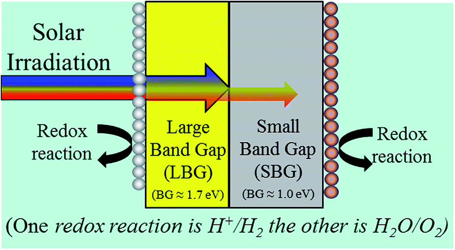 | ||
| Fig. 1 Generic design of a monolithic 2-photon water splitting device. | ||
• The 1st major design parameter is whether the LBG or SBG should act as a photoanode. Correspondingly, the other photoabsorber will then need to be able to work as a photocathode. Our goal is to determine the physical properties necessary for the photocathode and photoanode. We will then use computational screening to look for potential SBG and LBG candidate materials. This should allow us to analyse the feasibility of both designs.
• The 2nd major design parameter that will be analysed is light absorption properties of the redox catalysts with regards to device design. The H2 and O2 evolution catalysts can potentially absorb light meant for the photoabsorbers, thus decreasing efficiency. We will look at design parameters relating to a flat surface versus a pillared structure as well.
• The 3rd design parameter will be an analysis of operational pH. The commercial electrolyzer industry has shown that high ionic strength is necessary to minimize ohmic losses. Thus it is believed that either strongly acidic or strongly basic conditions are necessary.16 This parameter simply puts a difficult stability requirement for finding a LBG or SBG material.
• The 4th design parameter will be the analysis of attaching protective layers to the photoabsorbers. While the operational pH places severe constraints on material properties, the goal of the protection layers are to decouple stability from bandgap. Also the interfaces of protection layer/photoabsorber and protection layer/electrolyte-catalyst will be analysed.
Analysing which photoabsorber (LBG or SBG) should be the photocathode and which should be the photoanode is the overarching goal of this work. This will be done by investigating the materials used in literature as well as using a computational high-throughput screening technique to determine the potential feasibility of each approach. Issues such as device design, pH, device structuring, and protective layers all have major influences on the necessary material properties, thus they must be analysed to determine the necessary parameters needed for effective photoabsorbers.
For the readers who are interested in only specific areas, this work is broken down as followed:
• Section 1: device design and analysis for photocathodes, photoanodes and the interface between photoabsorbers.
• Section 2: analysis of potential photoabsorber candidates via computational screening and literature review.
• Section 3: light absorption of H2 and O2 evolution catalysts and different structurings.
• Section 4: protection layers: conductors, semiconductors, and insulators.
• Section 5: analysis of potential protected photoabsorber candidates via computational screening and literature review.
• Section 6: overall design viability and summary.
Section 1: device design
In Fig. 1 it is not specified which photoabsorber evolves H2 and which evolves O2. This is because either design may work as shown in Fig. 2. In Design 1 the O2 evolution takes place on the LBG and the H2 evolution takes place on the SBG. In Design 2, which seems less common in the literature, H2 evolution takes place on the LBG and the O2 evolution takes place on the SBG.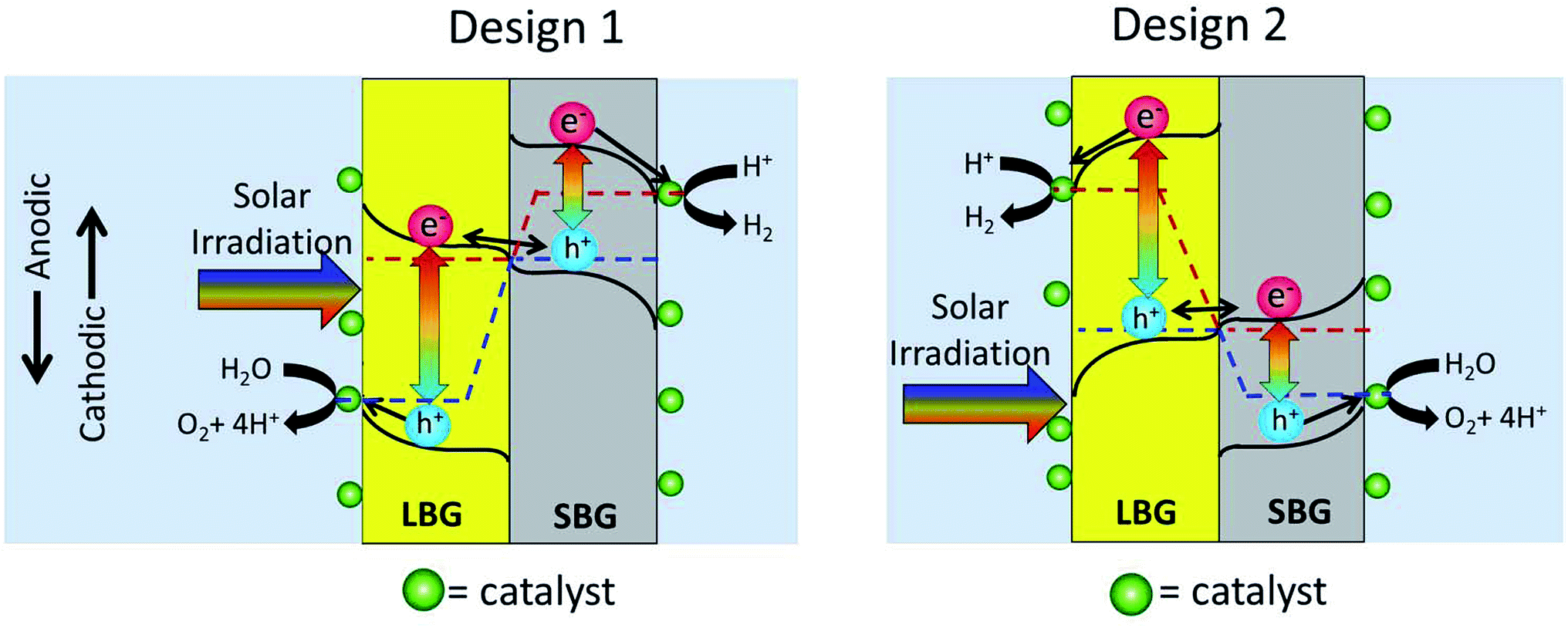 | ||
| Fig. 2 This figure shows two common approaches to a 2-photon tandem device. In Design 1 the large bandgap material (LBG) is on the O2 evolution side while the small bandgap (SBG) material is on the H2 evolution side. In Design 2 the LBG is on the H2 evolution side while the SBG material is on the O2 evolution side. | ||
Photoanode
With regards to the photoanode, the only difference between Design 1 and Design 2 is the size of the bandgap needed to accomplish O2 evolution. In Design 1 the photoanode will be the LBG and in Design 2 it will be the SBG. A key parameter in having an optimal photoanode is that the valence band (at the semiconductor/electrolyte interface) should be located near the O2 evolution potential. This potential corresponds to the thermodynamic potential plus overpotentials. Currently the best O2 evolution (OER) catalysts have an overpotential of 350 mV in pH = 14 and 300 mV in pH ≈ 0 (both @ 10 mA cm−2).17 This would entail that the optimal photoanode should have a valence band near 1.6 V vs. RHE (Relative Hydrogen Electrode). If the valence band were to be located much more anodic than 1.6 V vs. RHE, it would allow less efficient catalysts to be used, but it would also decrease band bending and thus decrease overall hole-extraction efficiency. A valence band slightly more cathodic than 1.6 V vs. RHE, would lead to inversion, which may prevent holes from populating any electronic states sufficiently anodic to evolve oxygen. Thus if one cannot find a material with an optimal valence band, it is typically favourable to error on the side of too anodic a valence band.One other very important parameter for photoanodes is their stability. These photoanodes need to be stable in the range of operating potentials that a 2-photon device may encounter as well as be stable in the dark. However in literature there is a discrepancy in what is being done in the labs and what is needed commercially. While lab tests are typically 1 hour or sometimes 24 hours, commercial devices will probably need to be stable on the order of years. Thus verifying long-term stability can be quite difficult. However the employment of techniques such as electrochemical quartz crystal microbalance testing (EQCM), inductively coupled plasma analysis (ICP) of the electrolyte and computational thermodynamic studies all can help bridge this gap in stability measurements.
Photocathode
Fig. 2 shows that the photocathode will be the SBG for Design 1 and the LBG for Design 2. The goal of the photocathode is to produce a photogenerated electron that is sufficiently cathodic to evolve hydrogen. The photocathode can be analysed in a similar manner as the photoanode. State of the art H2 evolution (HER) catalysts have an overpotential of approximately 50 mV in pH = 0 and 150 mV in pH = 14 (@ 10 mA cm−2).18,19 In the case of the photocathode the reductive electrons are migrating through the conduction band, thus the conduction band is the parameter of interest. Since the thermodynamic potential of H2 evolution is 0.00 V vs. RHE (by definition), the optimal conduction band position is at, or slightly cathodic of −0.05 V vs. RHE for pH = 0 or −0.15 V vs. RHE for pH = 14. Again, the material must be stable at the operating potentials for H2 evolution as well as being stable in the dark.Photoanode/photocathode interface
Proper design of the interface between the photoanode and photocathode is essential for any 2-photon water splitting device to function. In the dark the 2 photoabsorbers equilibrate their Fermi levels when they come into contact with each other. In the dark the Fermi level of a photoabsorber corresponds to the majority carrier potential, thus the majority carriers of the 2 photoabsorbers align. The equilibration of majority carriers' Fermi-level is shown in Fig. 2 as an alignment of the red dotted line in the photoanode and the blue dotted line in the photocathode.When the two stacked photoabsorbers are photoexcited so that the Fermi level splits into electron- and hole quasi-Fermi levels, the majority carrier Fermi levels should remain in equilibrium leaving the minority carrier quasi-Fermi levels to maximize their splitting (overall device photovoltage). For this reason there needs to be a highly selective contact between the two semiconductors, which only allows majority carriers to pass. One way to accomplish selective recombination of majority carriers is to connect the two photoabsorber materials via a tunnel junction, which has built-in band-bending barriers that block minority carrier flow, but permit majority carrier flow towards the junction. This can be done by locally doping the photocathode p++ and the photoanode n++ in the interface region. (++ stands for extremely highly doped.) This makes the interface hole-selective from the photocathode side and electron-selective from the photoanode side. By electronic tunnelling from n++ conduction band to the p++ valence band through the extremely thin depletion layer, the holes from the photocathode will annihilate the electrons from the photoanode as shown in Fig. 2. It should be noted that without the ++ layers an inadvertent p–n junction would form at the interface between the 2-photon absorbers. This inadvertent p–n junction would drive electrons and holes the wrong direction causing recombination of minority carriers, and thus destroy water splitting efficiencies.
For a more in-depth discussion and analysis of the photoanode, photocathode and interface the reader may consult the ESI.†
Section 2: computational screening for potential candidates for a 2-photon water splitting device
Now that we have analysed some of the necessary parameters needed for optimum materials for a 2-photon device, it would be quite useful it we could actually find potential candidate materials. In this section we look to accomplish this goal via a high throughput screening approach. In the last decades the search for new materials to use in different applications, such as batteries,20 scintillators,21 and photoabsorbers22-25 has been guided using computational screening approaches. Ab initio quantum mechanical simulations are able to reproduce experimental results with a good approximation and can be efficiently used to suggest new and interesting compounds. In previous works26,27 a high-throughput screening has been used to suggest 12 perovskites (5 oxides and 7 oxynitrides) for use as photoanodes in a 2-photon tandem device. In addition, 20 perovskites (10 oxides, 7 oxynitrides, and 3 oxyfluorides) that have been proposed for the one-photon scheme can also be used in the 2-photon device.26,27 However, in the current case pH stability is taken into consideration and the deviation from the optimal bandgap is reduced to more accurately show candidates which could achieve high solar to water splitting efficiency.Standard density functional theory performs poorly in predicting band gaps. To resolve this issue, we use the GLLB-SC functional27 that gives better agreement with experiments26 and with more computationally expensive methods like GW.28 The positions of the band edges are then calculated using an empirical equation based on the electronegativity of the constituents atoms.28 This method has been further described, validated and used in ref. 27 and 28.
For stability requirements, a compound was evaluated with respect to the possible known solid and dissolved phases in which it can dissolve.29,30 From this a Pourbaix diagram was calculated for each material. For a material to be a potential photoabsorber candidate, the material must ideally be thermodynamically stable (ΔE ≤ 0 eV per atom) at the given pH and operating potential of the redox reaction. Thus for a material to be accepted as a potential candidate, the parameter ΔE ≤ 0 eV per atom was used for all operating conditions. ΔE is the difference between the energy of the candidate material and of the most stable combination of other known materials (solid and dissolved phases) in which it can separate.
To effectively screen for materials a large database was generated by calculating the bandgaps of around 2400 compounds (which are experimentally known to exist) as described in the Materials Project database [http://www.materialsproject.org]. While the Materials Project database currently has 50![[thin space (1/6-em)]](https://www.rsc.org/images/entities/char_2009.gif) 000 materials that have been made experimentally, the bandgaps of all these materials have yet to be calculated using an accurate method, such as GLLB-SC or GW. Thus while the 2400 materials is only a subset of the database, it gives an adequate dataset to see general trends for potential candidates. For all materials that had indirect bandgaps, the indirect bandgap and band positions were used as the determining material parameters. The dataset is described in more detail in ref. 31. The data for all the bandgaps will be available in the Materials Project database and at the Computational Materials Repository (http://cmr.fysik.dtu.dk).
000 materials that have been made experimentally, the bandgaps of all these materials have yet to be calculated using an accurate method, such as GLLB-SC or GW. Thus while the 2400 materials is only a subset of the database, it gives an adequate dataset to see general trends for potential candidates. For all materials that had indirect bandgaps, the indirect bandgap and band positions were used as the determining material parameters. The dataset is described in more detail in ref. 31. The data for all the bandgaps will be available in the Materials Project database and at the Computational Materials Repository (http://cmr.fysik.dtu.dk).
We would like to stress that due to the computational methods and approximations applied the screening is not perfect. Earlier estimates show that the bandgap calculations for oxides are about 0.5 eV (ref. 26) and the relative stability calculations behind the Pourbaix diagrams may also show errors of 0.1 eV or more.29 Furthermore, all the calculations are non-spinpolarized meaning that (anti-)ferromagnetic materials are not treated correctly. Also the rather strict limits used for the screening mean that we may see both “false positive” and “true negative” material candidates. However the major point of this analysis is to show comparatively the number of potential candidates for different scenarios and for this purpose these calculations suite our needs.
Having identified possible candidates through the computational screening process, a quick literature review of each candidate was then done as a further filter. The literature review allowed for the removal of any candidates that have been experimentally proven not to meet the parameters set in Section 1. The raw computational screening data is shown in the ESI† as well as the detailed reasoning why any potential candidate was removed from that list.
Using the screening approach, the analysis in Section 1 was then used to choose reasonable parameters for the screening. While modelling studies have made it clear that an optimal device should have a LBG of ∼1.7 eV and a SBG of ∼1.0 eV, the above analysis has given little indication of what pH to use (pH = 0 or pH = 14) or which photoabsorber is favoured for which redox reaction (i.e. Design 1 or Design 2). Since theoretically any combination of pH and Design may work, all different possible combinations of Design and pH were screened.
In Section 1 it was determined that the optimal photoanode valence band would entail the computational screening should search for materials with a valence band of ∼1.6 V vs. RHE. In order to broaden our pool of potential candidates, the first parameter chosen was to search for all materials with a valence band more anodic than 1.6 V vs. RHE. This parameter may provide materials with band bending issues, but it will not allow any materials with inversion issues. It is also important that these materials be stable at the O2 evolution potential. Thus the second parameter chosen was that the candidates need to be stable in the range from 1.23 V vs. RHE until 1.8 V vs. RHE. The third parameter was that the material had to have a bandgap (Eg) close to either the optimal LBG (1.5 eV < Eg < 2.1 eV) or the optimal SBG (0.9 eV < Eg < 1.5 eV). While other parameters such as electron or hole mass, extinction coefficient, etc. could have been included, it was decided to use just these three parameters.
In Section 1 the optimal parameters for a photocathode conduction band were found. Applying these parameters, the first parameter was that the conduction band must be at or more cathodic than −0.05 V vs. RHE in acidic solutions or −0.15 V vs. RHE in basic solutions. The photocathode needs to be stable during H2 evolution conditions. Thus the second parameter was that the photocathode must to be stable in a range of 0.0 V vs. RHE to −0.4 V vs. RHE. The final parameter was that the material had to have a bandgap that either matched an optimal SBG or LBG. The photocathode bandgap conditions were the same as used for the photoanode.
The screening process was executed using the above mentioned parameters for all combinations of pH and Design. Table 1 shows all the results from the full screening process. By taking a quick glance at Table 1, it can be seen that there are few candidates. Even worse, almost all these candidates contain rare and expensive materials. The long term goal of photocatalytic water splitting is to provide a cheap renewable energy source to support the world's energy needs. It has been argued that the raw material needed to produce the photoabsorber needs to be able to be efficiently mined from the earth's crust.32 This realistically limits us to elements that are produced at rates of approximately 33 kt per year or more, which corresponds to the 40 most produced elements in the periodic table.32 By taking this into consideration, only 4 of the 41 unique materials listed in Table 1 are composed of materials based purely on the top 40 most produced elements.
| Design | pH | Screening parameters | Absorber (electrode) | # of candidates | Candidate materials |
|---|---|---|---|---|---|
| Design 1 | 0 | 1.5 ≤ EGap ≤ 2.1, VB > 1.6 V vs. RHE | LBG, (anode) | 6 | AuClO, Co(ReO4)2, Cr2Ag2O7, CuRhO2, Mg(BiO3)2, Zn(RhO2)2 |
| 0.9 ≤ EGap ≤ 1.5, CB < −0.05 V vs. RHE | SBG, (cathode) | 11 | As2Os, As2Ru, CdTe, FeSbS, GeAs, GeAs2, MoSe2, NaTiCuS3, KCuSe, SnSe, Te2Mo | ||
| 14 | 1.5 ≤ EGap ≤ 2.1, VB > 1.6 V vs. RHE | LBG, (anode) | 16 | Ag3VO4, AuClO, Au2O3, Ba2FeMoO6, Bi(III)3Bi(V)O7, Ca(RhO2)2, CdHgO2, Cd(RhO2)2, Cd2SnO4, Co(ReO4)2, Cr2Ag2O7, CuRhO2, Mg(BiO3)2, LaRhO3, LiBiO3, Zn(RhO2)2 | |
| 0.9 ≤ EGap ≤ 1.5, CB < −0.15 V vs. RHE | SBG, (cathode) | 2 | Ca3(CoO3) 2 , LaRhO3 | ||
| Design 2 | 0 | 1.5 ≤ EGap ≤ 2.1, CB < −0.05 V vs. RHE | LBG, (cathode) | 8 | CdSe, Cs2Ni3S4, InSe, NaHfCuSe3, NaPt2Se3, NaZrCuSe3, SbIrS, WSe2 |
| 0.9 ≤ EGap ≤ 1.5, VB > 1.6 V vs. RHE | SBG, (anode) | 2 | Bi2Pt2O7, HfNBr | ||
| 14 | 1.5 ≤ EGap ≤ 2.1, CB < −0.15 V vs. RHE | LBG, (cathode) | 1 | NaPt2Se3 | |
| 0.9 ≤ EGap ≤ 1.5, VB > 1.6 V vs. RHE | SBG, (anode) | 3 | Bi2Pt2O7, HfBrN, PtO2 | ||
Of the four materials that are composed solely of earth abundant materials, none have been studied intensely for photovoltaic applications. Recent theoretical work on FeSbS (e.g. gudmundite) has calculated its bandgap to be around 0.8 eV (ref. 33) in reasonable agreement with our calculation of 1.1 eV, however we were unable to find any experimental data verifying an exact bandgap value. To the best of our knowledge, only Ibers group has produced NaTiCuS3.34 In their work they noted it was a black color, which is what would be expected from a small bandgap material. Ba2FeMoO6 is a half metal, thus working with this material could provide some unique challenges.35 Ca3(CoO4)3 has been shown to have a bandgap of 1.3 eV,36 however its use as a photocatalyst may be hindered by the fact that it is magnetically frustrated.
Table 1 only had 3 parameters, so issues such as carrier lifetime and mobility of photogenerated electrons and holes are two major issues that were not taken into consideration. While to a certain extent this is related to experimental production of the materials, defect levels and effective mass of electrons and holes can be computationally determined. Adding these parameters may not theoretically rule out any material; however it could show that some materials will be very difficult to efficiently engineer. Another issue that was neglected in these calculations was whether these photoabsorbers could be either n-doped or p-doped. While many materials can be easily n-doped or p-doped, there are also a large group of materials (i.e. metallic oxides) that strongly favour one doping over the other.
While the above analysis paints a very pessimistic picture for using a 2-photon water splitting device, one must remember that the high-throughput screening only screened 2400 of the 50000 materials in the Materials Project Database. Also there is an uncertainty and error associated with the high throughput method so there is the possibility that the screening erroneously rejects some materials. The materials used in this database were all based on the bulk bandgaps. Quantization of photoabsorbers by variation in particle size is known to allow variations in bandgaps.37 This could be an alternative route to finding viable candidates. Another possible avenue to increase the number of potential candidates is to use a more moderate pH and find a creative way to minimize ohmic resistance between the anode and cathode.
One notable omission from Table 1 is Fe2O3, which has been shown to work as a LBG in Design 1 at pH = 14.38 With a band gap of 2.1 eV, this material was on the borderline meeting our parameters and the computational screening calculated the band gap to be too large. Fe2O3 has the potential to produce a 15% efficient device assuming the rest of the system is optimized.3 However, the extremely short hole diffusion length in Fe2O3 makes device engineering a major challenge.39,40 To date, the best reported photocurrent in Fe2O3 is 4.32 mA cm−2 at 1.23 V vs. RHE,41 although in principle the saturation current should be 12.6 mA cm−2.
As previously noted, the ideal LBG should have a band gap of ∼1.7 eV while the SBG should have a band gap of ∼1.0 eV. By including H2 and O2 evolution overpotentials using the best known catalysts, it takes approximately ∼1.7 eV to split water. Assuming that photovoltage is roughly proportional to the bandgap, the LBG should provide ∼63% of this value while the SBG material should provide the remaining ∼37%. If a reasonably efficient O2 evolution catalyst is used (ηA = 400 mV), a more appropriate metric for O2 evolution performance for an LBG, is the photocurrent at the expected operating point ∼0.67 V vs. RHE (1.7 V × 0.63 − ηA). At this, more realistic, applied potential Fe2O3 unfortunately only delivers a water oxidation current of ∼0.2 mA cm−2, which corresponds to ∼0.3% efficiency.41 This example illustrates the difficulty in trying to engineer a photoabsorber with fundamental limitations relating to electron–hole transport.
While the design parameters in Table 1 are for the near-optimal efficiency, any relaxation of this constraint naturally allows for more candidates. BiVO4 (ref. 42) and WO3 (ref. 43) have been two popular LBG candidates for Design 1, but their band gaps limit them to a maximum efficiency of 9%, and 8%, respectively. Experimentally BiVO4 has been shown to produce 2.3 mA cm−2 at 1.23 V vs. RHE, but it only produces ∼0.3 mA cm−2 at 0.67 V vs. RHE.44 WO3 has shown a respectable water oxidation current of ∼1.1 mA cm−2 at 0.67 V vs. RHE (tested at pH = 1).45 It should be noted that BiVO4 is only stable in base and WO3 is only stable in acidic solutions.
Even if Fe2O3, BiVO4 or WO3 was used, finding a successful matching earth abundant photocathode may not be easy. From our database of 2400 materials, Table 1 shows that our screening procedure only led us to find 3 earth abundant photocathode candidates for either the acidic or basic case. However, many researchers have looked to Si as a photocathode to try to accomplish this task.46 Si has a near-optimal band gap of 1.1 eV, and a conduction band near −0.5 V vs. RHE. Using Design 1 as directly shown in Fig. 2, the maximum onset potential Si could produce for H2 evolution was shown to be 0.2 V vs. RHE.46 This is significantly less than the 0.67 V vs. RHE necessary to equilibrate with an optimized LBG. This lack of photovoltage was shown to be a function of Si's inability to provide sufficient bandbending to separate electrons and holes.47 In Si, however, it is easy to make p–n homojunctions. Thus it is possible to resolve Si's flat-band potential limitation by creating a p–n homojunction.46,48 So far, this has led to an H2 evolution onset potential up to 0.52 V vs. RHE,18,46 thus there is still significant room for improvement. A more fundamental problem with Si (and the reason it is excluded from Table 1) is its poor stability. In base, Si is completely unstable.49 In acid, Si may be kinetically stable under H2 reduction conditions, but it suffers stability issues during dark conditions and even simply in air. Under real-world conditions the Si will always be exposed to a small amount of O2 from the anode or the ambient air. This has the possibility to slowly oxidize the photocathode over the long time periods used in commercial devices.50
While there is a strong international research effort for finding photoabsorbers for Design 1, relatively little work has been done directly focusing on Design 2 (as shown in Fig. 2). A rare example is GaP (Eg = 2.25 eV). By relaxing the optimal band gap constraint, GaP has been investigated as a LBG photocathode for Design 2.51 In this case it is the photocathode which should provide ∼63% of the photovoltage. Thus when using an efficient H2 evolution catalyst (ηC = 50 mV), a reasonable working potential at which to measure photocurrent is ∼1.02 V vs. RHE (1.7 × 0.63 − ηC). Kaiser et. al. have recently shown the maximum photovoltage for photocathodic H2 evolution current was only ∼0.5 V vs. RHE.51 Furthermore GaP is known to have imperfect stability in acid15 and its large bandgap constrains it to a maximum efficiency of 10%. It should be noted that Cu2O (Eg = 2.0 eV) has also been attempted as a Design 2 photocathode, however it is unfeasible to use this directly due to its instability in both acid and base.52 There has been no concerted effort to focus on SBG for Design 2.
The analysis in Table 1 shows that it is very difficult to find materials needed to meet the most basic parameters necessary in an optimized 2-photon water splitting device. A very brief survey of the materials being investigated for 2-photon water splitting show that the materials deviate significantly from the optimal bandgap, are unstable, are difficult to engineer or some combination thereof. By varying parameters in the computational screening process, it was discovered that photoabsorber stability in particular was a major limiting factor.
With photoabsorber instability being such a central issue, it would be extremely helpful if there was a way to mitigate this issue. Protection layers may provide such a solution. Protection layers are simply a layer of material that is inserted between the photoabsorber and catalyst/electrolyte. The protection layer prevents the electrolyte from interacting with the photoabsorber, which mitigates most stability problems of the absorber. The key advantage of using a protection layer is that it separates the stability issue from the photoabsorber issues (such as optimal band gap, electron–hole lifetime, etc.). From an engineering standpoint protection layers are typically much more forgiving on material impurity and defects since mechanical durability is typically a less fickle field than photovoltaic optimization. It should be mentioned that use of protection layers is not a new idea,53-57 however recent technological advances in deposition methods have made their usefulness re-emerge to the forefront.
While it may appear that using protection layers replaces PEC with ‘buried photovoltaics’ this is not always entirely true as will be shown later. Before discussing the necessary parameters for a protection layer, it is prudent to first consider miscellaneous issues such as catalyst light absorption properties and nanostructuring. Section 3 will analyse these issues while Section 4 will look into protection layer parameters.
Section 3: effects of catalysts and structuring of device
Fig. 3 shows a 2-photon water splitting device with redox catalysts on each side and a barrier preventing H2 and O2 crossover, but allowing ions (i.e. H+ in acid or OH− in base) to pass. In this figure, it's denoted that redox reactions take place on each photoabsorber. Whether this redox reaction is the H+/H2 reaction or the H2O/O2 reaction depends on the choice of Design 1 or Design 2 (see Fig. 2).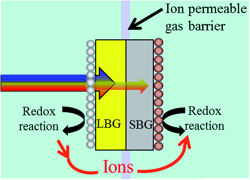 | ||
| Fig. 3 A 2-photon water splitting device that helps to illustrate issues due to light absorbing redox catalysts and length/thickness ratio issues. Which reaction takes place on which photoabsorber depends on whether a Design 1 or Design 2 approach is used (see Fig. 2). | ||
The diagram in Fig. 3 raises an issue that is sometimes neglected when discussing photocatalytic water splitting devices: the fact that redox catalysts may block incoming light to the photoabsorbers, thus decreasing device efficiency. Fig. 3 shows that the redox catalyst on the LBG will interfere with light absorption to the photoabsorbers whereas the redox catalyst on the SBG will not. From Fig. 2 it can be seen that Design 1 has the O2 evolution catalyst on the LBG and Design 2 has the H2 evolution catalyst on the LBG.
Recently the Boettcher group58 investigated the light absorbing properties of various O2 evolution catalysts. By modelling how their NiFeOx O2 evolution anode would perform in a photoelectrochemical solar cell, they found that an optimized device compromised ∼3.5% on light absorption and ∼40 mV of overpotential at 5 mA cm−2 (compared to a hypothetical thick NiFeOx catalyst layer with no light absorption issues). To obtain overpotentials within 5 mV of a thick NiFeOx layer more than 3 times that amount (∼10% light absorption) was needed. A thicker amount will be needed in commercial devices if there is even the slightest amount of catalytic corrosion. This result shows that a severe compromise must be made between catalyst activity and catalyst light absorption.
While there is no literature that has directly tested the optocatalytic properties of H2 evolution catalysts as directly as Boettcher's group, we are currently working on this and will report on this in the near future. However, recent photocathodic H2 evolution results indicate that H2 evolution catalysts have minimal impact on light absorption.18,48,59 Thus from the standpoint of catalyst light absorption, a LBG photocathode that evolves H2 would be favoured over an LBG photoanode that evolves O2. This clearly favours Design 2 over Design 1.
It should be noted that H2 evolution catalysts do not necessarily absorb less light than O2 evolution catalysts on a per mass or per layer-thickness basis. The absorption coefficients for RuO2 (O2 evolution catalyst) is actually slightly smaller than that of Pt (H2 evolution catalyst).60,61 However, the key difference is that the O2 evolution catalysts are much less efficient. In acid Pt has an exchange current density on the order of 10-4 A cm−2,62 while RuO2 only has an exchange current density on the order of 10−13 A cm−2.63 This, 9 orders of magnitude, difference in exchange current density entails that much more RuO2 needs to be used than Pt, thus explaining why light absorption is normally an issue for O2 evolution catalysts, but often not for H2 evolution catalysts.
While in Fig. 3 the length of the photoabsorber greatly exceeds the thickness, it is also possible to produce photoabsorbing pillars, which can simply be thought of as an inversion in the thickness to length ratio.47,64 This structuring approach does have the advantage of orthogonalizing light absorption to electron–hole diffusion, but this also means the redox catalysts will be orthogonalized. This results in having the catalysts on the sidewalls of the photoabsorbers rather than on the front and back of the photoabsorbers as shown in Fig. 3. This entails that the redox catalysts for both the LBG and SBG could potentially cause light absorption issues with the photoabsorbers. ESI† goes more into depth into this issue as well as protection layers for pillared structures.
Section 4: parameters and potential candidates for protection layers
Given that the primary purpose of the protection layers is to protect, the most important parameter is stability in the potential range that the protection layer will be operating in. In the search for potential photoanode candidates in Section 2 we suggested that realistic operating potentials of the photoanode will be in the range of 1.23–1.8 V vs. RHE. Therefore this is the approximate necessary stability range for an anode protection layer (APL). To help parameterize the cathode protection layer (CPL), the practical operating potential range of a photocathode that was suggested in Section 2 can be used. This means the CPL should be at least stable in the range of −0.4 to 0.00 V vs. RHE. While both protection layers also need to be stable at dark conditions, this is a hard parameter to define, thus this will remain undefined in this analysis.Three other major requirements for a protection layer is that it needs to be conductive, not absorb light at the relevant wavelengths and have either a negligible or positive effect on the photoabsorber's photovoltage. (The photovoltage issue is discussed in Section 5 and a thorough literature review is given by Liu et. al.)65 These properties depend on the type of material. To try to cover all situations, three general categories will be analysed: conductors, semiconductors and insulators.
Conductors
Since protection layers only need to be on the order of nanometers thick, there should be no issues with conductivity among conductors. However, light absorption is a much larger issue. Since, by definition, a conductor has its Fermi level in an unfilled band, it should broadly absorb light. Conductors typically have high absorption coefficients, thus even a thin layer will absorb significant amounts of light. Using Pt as an example, theoretically a 10 nm film should absorb approximately 55% of the photons coming from an AM1.5 spectrum.61 Thus conductor-based protection layers will only be effective if they are not located in-between the incoming light and the photoabsorbers. By looking at Fig. 3 it should be apparent that a conductive protection layer on the LBG would probably not work due to light absorption issues. However a protection layer on the SBG should definitely be viable since there are no light absorption restrictions on the shadow-side of the device.If it is assumed that device structuring does not give light absorption issues, we can look for potential conducting protection layers. In general, most metals oxidize in aqueous solutions (or even air), thus limiting the number of stable candidates. However, oxidation is not necessarily a bad thing for an anode protection layer (APL). All the state of the art O2 evolution catalysts are metallic oxides (RuO2, IrO2, Mn2O3, Co3O4, Ni0.9Fe0.1Ox, Ba0.5Sr0.5Co0.8Fe0.2O3–δ (ref. 66–69)). Thus if the metal state of one of these catalytic oxides is deposited as the APL, then their surface oxidation can also act as the O2 evolution catalyst. A film consisting purely of an O2 evolution catalyst could in principle also be used as an APL. However, using a metal interlayer before the O2 evolution catalyst typically gives less interface problems, such as oxidizing the photoabsorber, which makes device engineering easier.
Of the few metals that do not have oxidation issues, many of these are also good H2 evolution catalysts such as Pt at pH = 0, or Ni and Mo at pH = 14. Similar to the APL, a cathode protection layer (CPL) made from one of the aforementioned materials could act as both a protection layer and a catalyst. Pt is an interesting case though due to its extreme efficiency in catalysing the H2 evolution reaction. The amount of Pt needed in a photoelectrolysis device to evolve H2 evolution at sufficiently low overpotentials (<50 mV) theoretically can be less than a tenth of a monolayer.70 Since such a small amount of Pt may be needed, using it as a protection layer would be quite wasteful.
There are certain metals that are good protection layers even though they aren't efficient catalysts. By looking at the Pourbaix diagrams of metals, the general conclusion is that noble metals such as Au, Ag, etc. are the only pure materials that are effective protection layers. While precious metals may work, they would almost certainly fail due to economic and scalability reasons.
Semiconductors
While previously in this analysis the focus was on semiconductors as light absorbers, in this section the focus is now shifted to semiconductors as protection layers. In this application, the goal is for the semiconductors to have a large enough bandgap so they do not absorb any light meant for the photoabsorbers. Fig. 3 allows us to look at what parameters need to be set for each case. The protection layer on the LBG must not absorb any incoming solar irradiation. This entails that the bandgap be larger than ∼3.0 eV. On a SBG, there are no bandgap restrictions.The next issue to consider is the conductivity of semiconductor protection layers. In traveling long distances the conductivity through the bulk of a semiconductor can be a major issue. However, a protection layer will probably be less than 100 nm thick, thus even with low dopant densities bulk conductivity will probably not be an issue.18 While bulk conductivity may be unproblematic, conductivity of a protection layer at the surface/electrolyte interface is a major issue due to band bending. Depletion layers forming spontaneously at the semiconductor/electrolyte interface is beneficial for photoabsorbers since it prevents the majority carrier from reaching the electrolyte. However a semiconductor protection layer needs to be in the dark, thus it only offers majority carriers for electrical conduction. Thus in a protection layer, one must prevent a depletion layer from occurring. This can be done by either being at the flat band potential or going into accumulation mode. Accumulation mode simply means majority carrier charge will flow to the surface. Accumulation modes differ from the inversion modes discussed in Section 1 because in this case the majority carrier will be accumulating at the surface rather than the minority carrier. Since there are orders of magnitude more majority carriers than minority carriers, issues regarding lack of carriers at the surface are much less problematic in this case. (Using a semiconductor in a photoelectrochemical device without photoexciting the semiconductor is non-typical and thus may produce counterintuitive results.)
Determining the necessary parameters to have the protection layer go into accumulation mode depends on whether the photoanode or photocathode is being protected. Fig. 4 looks at the anode protection layer (APL) and shows both the case where the APL is in depletion mode (Fig. 4A) and accumulation mode (Fig. 4B). This figure illustrates how a depletion layer prevents charge transfer, and how an accumulation layer allows it.
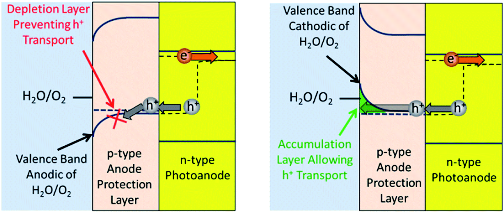 | ||
| Fig. 4 Schemes showing an APL that has a valence band (A) anodic and (B) cathodic of the H2O/O2 redox potential. These schemes show why the APL needs to be cathodic of the H2O/O2 redox potential to transfer holes without incurring issues from a depletion layer. The photoanode/APL interface is shown as a Schottky-interface for the purposes of simplicity. | ||
Using Fig. 4 as a guide, the conditions needed to have accumulation in an APL can be analysed. To conduct through the valence band the majority carrier needs to be holes, thus it needs to be a p-type material. Fig. 4 shows that to achieve accumulation in the APL, the APL's bulk valence band must be more anodic than its surface valence band. The bulk Fermi level of the APL should equilibrate with the hole quasi-Fermi level of the photoanode. Since the hole quasi-Fermi level provides the driving force for O2 evolution, the hole quasi-Fermi level's potential will be located at the O2 evolution potential. This is the thermodynamic potential (1.23 V vs. RHE) plus the overpotential (∼350 mV). Thus if the bulk valence band is located near 1.6 V vs. RHE, the surface valence band needs to be more cathodic than this to allow for an accumulation layer. Since the surface valence band is a function of the material, a material should have a valence band more cathodic than 1.6 V vs. RHE. However, if the valence band is located too anodic, there may not be enough density of states in the semiconductor to allow sufficient hole transfer. Another point of note is that a semiconductor may conduct charge to the surface even if the material is weakly in depletion due to trap sites at the surface.18,71 Taking these last two points into consideration, 1.1–1.8 V vs. RHE was used as the appropriate range for an APL valence band when searching for potential candidates.
In the case of the cathode protection layer (CPL) electrons are being transferred at highly cathodic potentials, thus it is more favourable to go through the conduction band. This means that the semiconductor must be n-type. To achieve an accumulation layer in the CPL, the situation and reasoning is simply the inverse of the APL. This means that the CPL's conduction band needs to be at or more anodic than the potential where H2 evolution occurs. However at potentials significantly anodic of the potential where H2 evolution occurs, the CPL may be lacking enough electronic states, and potentials slightly cathodic of the H2 evolution potential may still allow for conduction through the slight depletion layer. Thus in an attempt to find potential CPL candidates, −0.2 to 0.4 V vs. RHE was chosen as the appropriate range for a CPL conduction band.
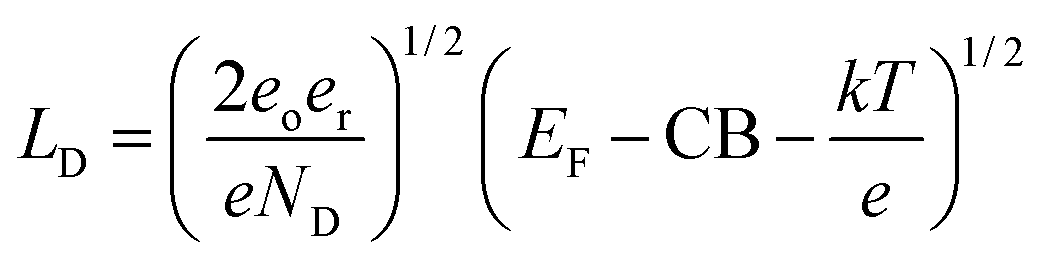
Potentially the issue with depletion layer could be mitigated by making the protection layer thinner than the depletion layer. The depletion layer thickness for an n-type material can be found viaeqn (1).
 | (1) |
Using the previously determined selection criteria for light absorption and band levels of semiconductors, it is relatively easy to find effective CPL candidates. While Honda and Fujishima's seminal work on photocatalytic water splitting basically started this field,72 two major issues with the TiO2 catalyst they used was that it barely absorbed any light from the solar spectrum and its conduction band was too close or potentially more anodic than the H+/H2 evolution potential. However these are prime conditions for a CPL, thus many researchers are investigating this approach.18,73,74 Furthermore, TiO2 is naturally n-type, which is a necessary condition for a CPL. Recently Seger et al. has shown stability for at least 30 days using a TiO2 CPL in acidic solutions.75 While Lin et al. has only tested TiO2 as a protection layer in basic solutions for 12 hours,66 TiO2 is well known to be extremely stable in base.76 Due to TiO2's promise as a CPL, there has been little effort to try anything else, but several good candidates exist. As an example, Nb2O5 has the proper conduction (−0.3 V vs. RHE) band position and a large bandgap (3.5 eV)77 and is stable in acid.78
With the possibility to use metals as a protection layer on the SBG, it may appear that there is little need to investigate semiconducting CPL for the SBG. However MoS2 provides an interesting case. With a band gap of 1.75 eV and a conduction band near 0.0 V vs. RHE,79 MoS2 is a very convenient CPL for the SBG since it also can be an effective H2 evolution catalyst and thus serve the double role of CPL and catalyst. Using MoS2 in this role has recently been tested.80 No issues with MoS2's ability to work as a protection layer were identified and the overall performance was promising after surface modifications were made to improve the density of catalytically active sites. Another abundantly available H2 evolution catalyst, Ni2P,81 is also a semiconductor with a bandgap near 1.0 eV and a conduction band near the H2 evolution potential.82,83 While yet untested, this also may have the potential to act as a dual function protection layer/H2 evolution catalyst. A special advantage in having a dual function protection layer/catalyst is that even if this layer corrodes at a manageable rate (∼1 monolayer per month), a thick layer may still allow continued catalytic activity even as the protection layer slowly corrodes. The protection layer's thickness could then just be a function of the designed service-life of the device.
While it is relatively easy to identify promising CPL's, the quest for APL's is much tougher. In this case, the material needs to withstand oxidizing conditions (1.23–1.8 V vs. RHE) while having a relatively cathodic valence band (1.1–1.8 V vs. RHE) and a large band gap. Due to the oxidizing conditions there is typically a thermodynamic driving force for any material to convert to oxides. The oxygen 2p orbital is located at approximately 3.0 V vs. RHE and most oxides valence bands are primarily based on this orbital.84 This eliminates a large number of candidates. However oxides such as Cu2O,85 NiO,86 CoO,86 and BiO87 have a valence band that is primarily based on a metallic d or s orbitals rather than the O2p orbital. This results in valence bands that are typically much more cathodic than the O2p. This increased valence band typically results in materials with smaller bandgaps.
However with a bandgap of 3.7 eV, NiO is a notable exception.88 NiO is naturally p-type, relatively stable in base (but not an acid) thus it has many of the characteristics of a potential APL. Since its valence band is located at ∼1.0 V vs. RHE,88 it would need to either operate heavily into accumulation mode or its band may become depinned. Furthermore due to its complicated electronic structure NiO is relatively inefficient at transporting holes.89–91 Doping it to increase conductivity can lead to the production of metallic nickel, which turns the material black.92 Thus while this material may have potential as a transparent APL, it also has many issues it needs to overcome.
To take a more thorough approach to find potential APL candidates, we used the screening method previously employed for finding potential candidates for photoanodes and photocathodes. This allowed us to screen through 2400 candidates, using the aforementioned stability and light absorption parameters (Eg > 3.0 eV). From this screening we found only Ca2PdO6 as an APL candidate and the calculations showed it is only stable in basic conditions. (The raw computational data is in ESI.†) However, Ca2PdO6 contains Pd (which makes it unlikely to be scalable) and it has only been produced using high pressure (100 kbar) synthesis techniques, therefore the prospects for using this material as an APL are poor. From Fig. 3, it is essential that the protection layer's bandgap is large enough to prevent light absorption to the front photoabsorber. Fig. 2 shows that Design 1 would need an APL on the front photoabsorber. Thus from this analysis, there is currently no simple path to using a semiconducting APL in Design 1.
While there are no bandgap limits for an APL on the SBG side, boron phosphide (BP) is an interesting APL candidate due to its stability in acid and base (Eg = 2.0 eV, valence band 1.44 V vs. RHE).93 To conduct through the valence band it needs to be p-type, however it is typically n-type. While n-type BP has been used as a CPL93 and an APL by degenerately doping it,57 interestingly BP has never been used as an APL by conducting through its valence band.
Manganese oxide has been tested as protections layer by multiple groups. This approach has been attempted by both sputtering manganese oxide and depositing manganese oxide via atomic layer-deposition on n-Si for O2 evolution.53,94 As Strandowitz et al. points out though, these materials have significant ohmic resistance and may naturally be unstable as an APL due to their tendency to become porous from redox cycling.94
During the process of publication, Hu et al. has published a work that uses a Ni influenced TiO2 as a photoanode protection layer.95 While the authors appear unsure of the exact mechanism for why this works, they believe it is due to defect sites throughout the bulk TiO2 and Ni intermixing with the TiO2 at the surface to help holes transfer through the surface barrier layer. However, currently this approach has issues with the external quantum yield and there is slight performance decay over time that is not yet understood. Thus while this approach provides a promising potential alternative route for semiconductor photoanode protection layers, there are still many issues that need to be understood and optimized to see if this method provides a valid alternative.
Insulators
Initially one would think that insulators would be completely ineffective as a protection layers for photoelectrochemical devices since they cannot conduct current. However, if the layer is sufficiently thin, it is possible to tunnel through an insulator. Thus, for the purpose of this analysis, insulators will be defined as any material that conducts only via electronic tunnelling. If one assumes a triangular tunnelling barrier, the net tunnelling current can be approximated by using the Wentzel–Kramers–Brillouin (WKB) approximation as shown in eqn (2):96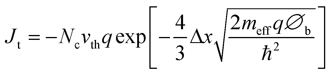 | (2) |
In this equation Jt is tunnelling current, ℏ is Planck's constant divided by 2π, q is the elementary charge, ∅b is the barrier height and Δx is barrier width, i.e. the tunnel distance. vth is the thermal velocity and Nc is the effective density of states.
The most important parameter in eqn (2) is the Δx because the tunnelling current will drop exponentially with an increase in distance. It should be noted that for semiconductors Δx corresponds to depletion length, not total thickness. Thus even a thick, but highly doped semiconductor layer has the potential to support tunnelling if the depletion layer is sufficiently thin. In most situations Δx needs to be limited to less than ∼3 nm to get sufficient tunnelling current.
∅ b is another important parameter that relates to tunnelling, and can also strongly influence the tunnelling current. For an APL, ∅b is analogously the potential difference between the insulator's valence band and the photoanode's hole quasi-Fermi level. For a CPL, ∅b is simply the potential difference between the insulator's conduction band and the photocathode's electron quasi-Fermi level. While these can be tuned slightly, the fact that only doubling Δx, has the same effect as a 4 times increase of ∅b means that Δx is the dominant parameter in eqn (2). This implies that barrier height, and hence conductivity, is only a minor parameter in the search for potential insulating candidates.
Insulators do have the benefit that their band structure is such that they do not absorb light in the solar spectrum so this is not a parameter that needs analysed. This means that it doesn't matter whether Design 1 or Design 2 is used. Thus the only critical property for an insulating protection layer is that it must be exceedingly stable at the operating potentials and pH of the redox reaction. Al2O3 is a well-known material that has already been tested as a CPL97 (pH = 0) and an APL98 (pH = 7). However Al2O3 is known to be slightly unstable in both acid and base, thus its long term durability is questionable.49 SrTiO3 has been show to work as an APL (pH = 13) as well.99
The big issue with insulating protection layers are their stability, and homogeneity. Producing a nanometer-thin, pinhole-free coating on a commercial scale may be technically possible, but the purity and consistency needed for this operation may ultimately prove to be impractical. In certain photoabsorbers, their surface can be oxidized to form a thin insulating layer of a stable material. Si oxidizing to SiO2 is an example of this. By oxidizing the photoabsorber directly, there is no need to worry about producing a pinhole free surface. However, producing a thin, uniform insulating layer, while not allowing further future oxidation, is rarely possible.
Summary of protection layers
In general there are many possibilities using metallic protection layers on the SBG side, however there is much less potential for using this on the large bandgap side. Metallic protection layers allows for possibility of a combined protection layer/catalyst layer. Semiconducting protection layers, have some restrictive parameters, which generally seems to limit them to cathodic protection layers. While there are stable and earth abundant insulating candidates, the fact that these materials must be extremely thin makes them a gamble from a durability and manufacturing consistency standpoint.In this analysis we chose distinct categories: conductors, semiconductors and insulators. There is also the possibility to have a protection layer that is a hybrid of these three approaches. While TiO2 is a semiconductor, Chen et al. recently used it in such a way that tunnelling was the primary method of charge transfer.100 However thicknesses beyond 2 nm showed noticeable ohmic resistance. There have been many examples where semiconductors or insulators have been highly doped to allow for electronic tunnelling,54,55,57,101 however long term stability is a difficult problem in many of these cases. For example, Contractor and Bockris used platinum doped SiO2 as a protection layer and it lasted 110 hours before starting to fail.54 The fact that this approach worked relatively well for 110 hours before rapidly failing reiterates the importance of long term durability studies since economically viable water splitting devices will need to be stable for years.10
Another approach that has yet to be discussed is the situation where only one side is protected. This approach may hold some promise if an excellent unprotected photoanode or photocathode is found. Analysing the necessary parameters for this situation would be relatively simple. The parameters for the unprotected side would be governed by the analysis in Section 1 and 2, whereas the parameters for the protected side would be based on the analysis from Section 4 and 5.
Wired devices, where one side of the water splitting device is attached to a transparent conductive glass, is a major example of where only one side needs to be protected. In these cases, light absorption is not a factor, thus a wide variety of protection layers could be used for either an electrolyte facing photoanode or photocathode.
Section 5: computational screening of potential protected photoabsorber candidates
In the case where protection layers have been used there are no general stability requirements for the photoabsorbers. The interface between the photoabsorber and protection layer needs to be stable, however this can only be judged on a case-by case basis and not a broad analysis such as this work.Since the photoabsorbers are in contact with protection layers rather than electrolyte, the band bending and optimal photoabsorber materials are functions of the protection layer and must be analysed accordingly. For this reason the potential photoabsorber candidates needs to be analysed for each group of protecting layers.
Conductors
A conductor/semiconductor interface should form either an ohmic contact or a Schottky contact. An ohmic contact means the conductor will equilibrate with the Fermi-level of the semiconductor, thus preventing photovoltage. In a Schottky contact the band bending is set between the work function of the conductor versus the dark Fermi level of the semiconductor. In principle, a conductor that has the proper work function could provide the necessary band bending to obtain optimal performance from a photoabsorber. However, the large number of electronic states that are inherent with conductors typically lead to an excessive recombination rate under operating conditions, which severely lowers the photovoltage.To resolve the issues with band bending/surface recombination at the conductor–semiconductor interface, the band bending can simply be shifted from the conductor–semiconductor interface to within the semiconductor. Typically, this means making a p–n homojunction within the photoabsorbers. For some photoabsorbers, such as Si, there is a well-known procedure how to do this, while in many other materials such as TiO2, this has proven to be difficult.
Using a metallic protection layer favours the approach where a p–n homojunction is made in the photoabsorber in order to mitigate surface recombination losses. In p–n junctions the surface may be so highly doped that tunnelling occurs.46 Since tunnelling is only a minor function of band position, it is unnecessary to have a parameter defining where these bands should be located.
If both stability and band positions are not an issue, the only parameter left is bandgap. Thus for the situation where the materials forms a p–n homojunction the same photoabsorbers will be relevant whether Design 1 or Design 2 is used or pH = 0 or pH = 14 is used. By using the same screening method as in Section 2, protected photoabsorber candidates could be found. The computational screening found 250 LBG and 209 SBG candidates. Due to the large number of candidates, a literature review filter was done on only the abundantly available candidates (i.e. production rate larger than 33 kton per year). The details of the filtering process are discussed in ESI.†Table 2 shows the filtered results of the abundantly available candidates for both the LBG and SBG.
| Design | Screening parameters | # of candidates | Candidates |
|---|---|---|---|
| SBG | 0.9 ≤ EG ≤ 1.5 | 51 | BaAs2, BaCaSn, Ba2Cu(PO4)2, Ba2FeMoO6, Ba3(Si2P3)2, BaLaI4, Ba3P4, CaBaSi, Ca3(CoO3)2, Ca2Si, Ca3SiO, CoAsS, CuCl2, CuP2, FeS2, FeSbS, K2Mo6S6, KNbS2, KPb, KSnAs, KZnAs, LaAs2, LaZnAsO, LaZnPO, LaS2, MgP4, MnP4, Na4FeO3, Na4FeO4, NaNbS2, NaNiO2, Na3Sb, NaSnP, NaTiCuS3, NaTiS2, NaZnP, NbFeSb, NbI3, Si, SnS, Sr2As2, Sr3As4, Sr3SbN, SrCaSi, SrCaSn, SrLaI4, Sr(ZnP)2, V(S2)2, Zn2Cu(AsO4)2, ZrBr3, ZrCl3 |
| LBG | 1.5 ≤ EG ≤ 2.1 | 50 | B, BP, BaCu2SnS4, Ba(MgSb)2, BaP3, Ba4Sb2O, Ba2ZnN2, Ca3AlAs3, Ca(BC)2, Ca3(BN2)N, Ca(MgSb)2, Ca Na10Sn12, Ca3VN3, Ca(ZnP)2, CoBr2, CuSbS2, Cu2O, Cu3VS4, FeBr2, FeSO4, Fe(SiP)4, I2, K3As, K2Ni3S4, K4P6, K3Na2SnAs3, K2NiAs2, KSb, KV(CuS2)2, KZnP, KCuZrS3, MgAs4, NaCuO2, NaNbN2, NaP, NaSbS2, Nb6F15, NbI5, SnZrS3, SrP, Sr3P4, SrPbO3, TiBrN, TiI4, TiNCl, Sn2TiO4, WBr6, ZnSiAs2, ZrCl2, Zr2SN2 |
Table 2 shows there are 51 potential candidates for the SBG and 50 for the LBG. Many of these materials such as Si,46,75 Cu2O,102,103 and SnS104,105 are already used in photoelectrochemical cells. This clearly shows that there are many potentials avenues for success by using a p–n junction photoabsorber in conjunction with a metallic protection layer. Additionally these same photoabsorbers can be used with semiconducting and insulating protection layers given they have a built in p–n junction.
Semiconductors
Using a semiconducting protection layer allows a unique situation to occur with regards to photoabsorber band bending. From the analysis in Section 4 it was determined that the APL needs to be p-type while the photoanode is n-type. Correspondingly the CPL needs to be n-type while the photocathode needs to p-type. Thus by default, there is a p–n heterojunction between the photoabsorber and the protection layer. This ability to possibly use the protection layer to also help in photoabsorber band bending shows that protected photocatalytic water splitting devices can be more than simply a ‘buried photovoltaic’.The initial key to maximizing the band bending from this p–n junction is to make sure the band diagrams of the photoabsorber and protection layers are aligned properly. In this analysis it is assumed that the conduction band offset will be given by the difference between electron affinities. (ESI† discusses this more in-depth.) This means optimal band bending will occur when the electron affinities (i.e. conduction bands at the flat band potential) of the photocathode and CPL align. Analogously the optimal band bending for the photoanode will take place when the valence bands (at the flat band potential) of the photoanode and APL align.
Determining these parameters for the photocathode is quite simple. Since in Section 4, we denoted that the conduction band of an n-type semiconducting CPL needs to be near the H+/H2 redox couple, this would mean that the conduction band of the p-type photoabsorber would need to be the same. Thus we can take the candidates found in Table 2 and filter them with the requirement that the conduction band must be more cathodic than 0.00 V vs. RHE. This allows us to get potential photocathode candidates without the use of a p–n homojunction as shown in Table 3. Using a similar logic the valence bands of the n-type photoabsorber and p-type semiconducting APL should align to maximize the potential for band bending. In Section 4 our analysis showed the valence band for a semiconducting APL needs to be near 1.6 V vs. RHE. Thus in this case a photoanode's valence band should be at or more anodic than 1.6 V vs. RHE. Table 3 shows these potential candidates as well. The computational modelling shows that CuSbS2 has a band diagram that could potentially allow both H2 and O2 evolution. However it probably couldn't work as a 1-photon water splitting due to the inherent ∼400 mV loss due to thermodynamics as mentioned in the introduction.
| Design | Photo-absorber | Screening parameters | # of candidates | Candidates |
|---|---|---|---|---|
| 1 | LBG, (photoanode) | 1.5 ≤ EGap ≤ 2.1, VB > 1.6 V vs. RHE | 16 | CoBr2, CuSbS2, FeBr2, FeSO4, I2, Nb6F15, NbI5, SnZrS3, TiBrN, TiI4, TiNCl, Sn2TiO4, WBr6, ZrCl2, ZrCl3 Zr2SN2 |
| 1 | SBG, (photocathode) | 0.9 ≤ EGap ≤ 1.5, CB < 0.0 V vs. RHE | 6 | BaLaI4, CuP2, FeAs2, FeSbS, MgP4, SnS |
| 2 | LBG, (photocathode) | 1.5 ≤ EGap ≤ 2.1, CB < 0.0 V vs. RHE | 3 | CuSbS2, NaCuO2, Zr2SN2 |
| 2 | SBG, (photoanode) | 0.9 ≤ EGap ≤ 1.5, VB > 1.6 V vs. RHE | 8 | Ba2Cu(PO4)2, Ba2FeMoO6, CuCl2, CuP2, NbI3O, V(S2)2, Zn2Cu(AsO4)2, FeS2 |
The uncertainty in the exact potential of the protection layer and the uncertainty in assuming the band offset is purely a function of electron affinities means that Table 3 is a quite rough estimate of potential candidates. Nevertheless this table show that there are earth abundant candidates for both the SBG and LBG for both designs. While Table 3 shows that without the p–n homojunctions, there are significantly less candidates, there are still many more earth abundant candidates than for the unprotected case. (Table S4 in ESI† shows the computational screening results without the literature review filter.)
While proper band alignment allows the possibility for optimal band bending, proper doping is needed to ensure maximum band bending. The total band bending voltage will be the difference in dark Fermi levels between the n-type and p-type material. This band bending and corresponding depletion layer will be distributed between both semiconductors. Since the photoabsorber needs to separate electron–holes pairs and the protection layer does not, it is beneficial to try to force the majority of the band bending into the photoabsorber. The thickness of the band-bending region is inversely proportional to the square root of the dopant density, thus the protection layer should be highly doped with respect to the doping level of the photoabsorber. A minimally doped photoabsorber gives less bulk recombination, whereas a highly doped protection layer increases conductivity to the electrolyte/catalyst. This is a win-win situation, which has already been shown to be quite effective.106
It should be noted that practical difficulties may occur at the protection layer/photoabsorber interface. These include lattice mismatch, defects and dangling bonds, poor adhesion, etc. Such problems may result in fabrication difficulties or high surface-recombination of electron–hole pairs. However, such practical issues can only be judged on a case-by-case basis, therefore they are unsuited for a broad analysis such as this work.
Insulators
In the case of an insulating protection layer, the electron tunnels from the photoabsorber to the electrolyte/catalyst. If the catalyst covers a sufficiently large area of the protection layer, it will most probably resemble a metal/insulator/semiconductor interface (assuming the catalyst is metallic) and act according to those principles. Chen et al.104,105 and Kenney et al.107 have shown this technique to produce significant photovoltage. If the catalyst does not cover a significant portion of the electrolyte interface, the catalyst will effectively get ‘pinched off’ from having any effect of the electronic structure of the system.108 In this case the photoabsorber/insulator/catalyst/electrolyte system will be dominated by the photoabsorber/electrolyte interactions and Fermi level equilibration.In the pinched off case the photoabsorber band diagram will be pinned and the analysis will be analogous to the unprotected case. (The ESI† goes into more detail.) Thus the conduction band should be slightly cathodic of 0.0 V vs. RHE and the valence band should be at or slightly more anodic than 1.6 V vs. RHE. These conditions are very similar to the semiconducting protection layer case. Thus Table 3 is also a relatively good approximation for potential photoabsorber candidates using a photoabsorber with an insulating layer and no p–n homojunction.
Only 2400 materials were used in this analysis, and some known semiconductors with optimal bandgaps were not included in this list such as Zn3P2 (Eg = 1.5),109 and the very enticing PbI type perovskites.110 Furthermore the 2400 materials were screened by a high-throughput method whose accuracy is compromised by the large number of candidates. Thus Tables 2 and 3 (as well as Table 1) are not meant to be a definitive list of photoabsorber candidates. Undoubtedly there are potential photoabsorber candidates that these tables have missed (e.g. AlSb with an Eg = 1.7 eV),111 and certain materials on these tables may not have the properties the computational modelling predicted and slipped through the literature review filter. However, the purpose of these tables is to show general trends in availability of materials with the necessary parameter needed for a 2-photon water splitting device. For that purpose the larger number of abundantly available candidates in Table 2 and 3 compared to that in Table 1 clearly demonstrates the beneficial role which protection layers may play in helping identify a commercially viable approach to 2-photon water splitting devices.
Section 6: overall summary and design viability
While the protected photoabsorber candidates (Section 5) clearly outnumber the unprotected candidates (Section 2), Section 4 indicates that finding acceptable protection layers is not a trivial task. The general conclusion is that metal protection layers would only work on the SBG, semiconductor protection layers have been shown to work best on the photocathodes, and insulating protection layers need to be very thin. In Section 1 we defined 2 Designs, which differed only in which redox reaction occurred on which photoabsorber (LBG or SBG).Design 1 has a LBG photoanode and a SBG photocathode. There are clear ways to provide a thick protection layer on the SBG photocathode, but so far there has not been any well tested way to provide a thick protection layer for the LBG photoanode in Design 1. From the present analysis, protection of a LBG photoanode would currently have to rely on tunnelling through an insulating protection layer (or potentially defect states in TiO2).43,100 On the other hand, Design 2 has a LBG photocathode and a SBG photoanode. In this design there are proven strategies to provide thick protection layers on both sides of such a device as was demonstrated in Section 4. This gives Design 2 a tremendous advantage over Design 1. Moreover, in Section 3 we argued that light absorption issues from the H2 and O2 evolution catalysts probably favour Design 2 over Design 1. While Design 1 may be workable, from this analysis Design 2 currently appears to provide more avenues to produce a practical device.
Fig. 5 shows Design 2 with a semiconducting cathode protection layer, a p–n homojunction photoanode and a metallic protection layer that oxidizes into a catalyst layer.
 | ||
| Fig. 5 This figure shows a flat structured 2-photon water splitting device with a semiconducting CPL, a large bandgap photocathode, a small bandgap p–n homojunction small bandgap photoanode, and a metallic anode protection layer that converts into a thin film O2 evolution catalyst. | ||
Many of the parts in Design 2 has already been created and tested. TiO2 has been shown to be quite effective as a cathode protection layer.103,106,112,113 Si, with a bandgap of 1.1 eV is an almost ideal SBG and can very easily create p–n homojunctions.18,46,107 It has also recently been shown that a metallic protection layer can be deposited onto Si, and its surface oxidation can act as a catalyst.107
Section 4 showed that a protected Design 2 device can be stable in both acidic and basic conditions. At this point it becomes a matter of which pH the redox reaction favours. For the H2 evolution, Pt is an excellent catalyst in both acid and base.114 There are also efficient earth abundant catalysts in acid (MoS2, Ni2P)48,81 and in base (Ni, NiMoN).115,116 For O2 evolution, there are many efficient earth abundant catalysts in base, but so far only IrO2 is a stable catalyst in acid.17 Thus currently, the catalyst choice favours basic conditions over acidic conditions.
The effects of inadvertent light absorption by redox catalysts strongly favours Design 2 over Design 1 due to the greater efficiency of H2 evolution catalysts compared to O2 evolution catalysts. Creating photoabsorbing pillars (rather than a flat photoabsorber) orthogonalizes light absorption with respect to electron–hole extraction; however it also orthogonalizes the light absorbing properties of the redox catalysts and potentially any protection layers.
In summary, the present analysis focusses on the thermodynamic parameters necessary for materials used in a monolithic 2-photon water splitting device. By assuming current state of the art H2 and O2 evolution catalysts, we developed quantitative thermodynamic parameters that was used to look for potential candidates using computational screening. The goal of the high-throughput screening was not to find the perfect candidate materials, but rather to illustrate which parameters (e.g. Design, pH, structuring, protected/unprotected) allow for the largest pool of potential candidates, thus indicating the most promising research strategy.
Acknowledgements
We gratefully acknowledge the Danish Ministry of Science for funding the Catalysis for Sustainable Energy (CASE) initiative, the Danish National Research Foundation for funding The Center for Individual Nanoparticle Functionality (CINF) (DNRF54). Support was also obtained from the Center on Nanostructuring for the Efficient Energy Conversion (CNEEC) at Stanford University, an Energy Frontier Research Center founded by the US Department of Energy, Office of Science, Office of Basic Energy Sciences under award number DE-SC0001060.Notes and references
- M. F. Weber and M. J. Dignam, Int. J. Hydrogen Energy, 1986, 11, 225–232 CrossRef CAS.
- S. Haussener, C. Xiang, J. M. Spurgeon, S. Ardo, N. S. Lewis and A. Z. Weber, Energy Environ. Sci., 2012, 5, 9922–9935 CAS.
- S. Hu, C. Xiang, S. Haussener, A. D. Berger and N. S. Lewis, Energy Environ. Sci., 2013, 6, 2984–2993 CAS.
- M. C. Hanna and A. J. Nozik, J. Appl. Phys., 2006, 100, 074510 CrossRef PubMed.
- A. B. Laursen, S. Kegnaes, S. Dahl and I. Chorkendorff, Energy Environ. Sci., 2012, 5, 5577–5591 CAS.
- L. C. Seitz, Z. Chen, A. J. Forman, B. A. Pinaud, J. D. Benck and T. F. Jaramillo, ChemSusChem, 2014, 7, 1372–1385 CrossRef CAS PubMed.
- M. D. Archer and J. R. Bolton, J. Phys. Chem., 1990, 94, 8028–8036 CrossRef CAS.
- S. Haussener, S. Hu, C. Xiang, A. Z. Weber and N. S. Lewis, Energy Environ. Sci., 2013, 6, 3605–3618 CAS.
- W. Shockley and H. J. Queisser, J. Appl. Phys., 1961, 32, 510–519 CrossRef CAS PubMed.
- B. D. James, G. N. Baum, J. Perez and K. N. Baum, Technoeconomic Analysis of Photoelectrochemical (PEC) Hydrogen Production, Directed Technologies Inc., 2009, p. 128, https://www1.eere.energy.gov/hydrogenandfuelcells/pdfs/pec_technoeconomic_analysis.pdf Search PubMed.
- D. G. Nocera, Acc. Chem. Res., 2012, 45, 767–776 CrossRef CAS PubMed.
- M. Graetzel, M. Gratzel and P. Liska, Hydrogen Solar Ltd, WO2007066087 A2, 2007.
- M. Gratzel, Nature, 2001, 414, 338–344 CrossRef CAS PubMed.
- A. J. Nozik, Appl. Phys. Lett., 1977, 30, 567–569 CrossRef CAS PubMed.
- O. Khaselev and J. A. Turner, Science, 1998, 280, 425–427 CrossRef CAS.
- J. R. McKone, N. S. Lewis and H. B. Gray, Chem. Mater., 2014, 26, 407–414 CrossRef CAS.
- C. C. L. McCrory, S. Jung, J. C. Peters and T. F. Jaramillo, J. Am. Chem. Soc., 2013, 135, 16977–16987 CrossRef CAS PubMed.
- B. Seger, T. Pedersen, A. B. Laursen, P. C. K. Vesborg, O. Hansen and I. Chorkendorff, J. Am. Chem. Soc., 2013, 135, 1057–1064 CrossRef CAS PubMed.
- R. Subbaraman, D. Tripkovic, D. Strmcnik, K.-C. Chang, M. Uchimura, A. P. Paulikas, V. Stamenkovic and N. M. Markovic, Science, 2011, 334, 1256–1260 CrossRef CAS PubMed.
- G. Ceder, Y. M. Chiang, D. R. Sadoway, M. K. Aydinol, Y. I. Jang and B. Huang, Nature, 1998, 392, 694–696 CrossRef CAS PubMed.
- W. Setyawan, R. M. Gaume, S. Lam, R. S. Feigelson and S. Curtarolo, ACS Comb. Sci., 2011, 13, 382–390 CrossRef CAS PubMed.
- N. M. O'Boyle, C. M. Campbell and G. R. Hutchison, J. Phys. Chem. C, 2011, 115, 16200–16210 Search PubMed.
- R. Olivares-Amaya, C. Amador-Bedolla, J. Hachmann, S. Atahan-Evrenk, R. S. Sanchez-Carrera, L. Vogt and A. Aspuru-Guzik, Energy Environ. Sci., 2011, 4, 4849–4861 CAS.
- W.-J. Yin, H. Tang, S.-H. Wei, M. M. Al-Jassim, J. Turner and Y. Yan, Phys. Rev. B: Condens. Matter Mater. Phys., 2010, 82, 045106 CrossRef.
- M. d’Avezac, J.-W. Luo, T. Chanier and A. Zunger, Phys. Rev. Lett., 2012, 108, 027401 CrossRef.
- I. E. Castelli, T. Olsen, S. Datta, D. D. Landis, S. Dahl, K. S. Thygesen and K. W. Jacobsen, Energy Environ. Sci., 2012, 5, 5814–5819 CAS.
- I. E. Castelli, D. D. Landis, K. S. Thygesen, S. Dahl, I. Chorkendorff, T. F. Jaramillo and K. W. Jacobsen, Energy Environ. Sci., 2012, 5, 9034–9043 CAS.
- I. E. Castelli, J. M. Garcia-Lastra, F. Hüser, K. S. Thygesen and K. W. Jacobsen, New J. Phys., 2013, 15, 105026 CrossRef.
- I. E. Castelli, K. S. Thygesen and K. W. Jacobsen, Top. Catal., 2014, 57, 265–272 CrossRef CAS PubMed.
- K. A. Persson, B. Waldwick, P. Lazic and G. Ceder, Phys. Rev. B: Condens. Matter Mater. Phys., 2012, 85, 235438 CrossRef.
- I. E. Castelli, F. Hüser, M. Pandey, H. Li, B. Seger, K. S. Thygesen, A. Jain, K. Persson, G. Ceder and K. W. Jacobsen, 2014, submitted.
- P. C. K. Vesborg and T. F. Jaramillo, RSC Adv., 2012, 2, 7933–7947 RSC.
- D. Parker, A. F. May, H. Wang, M. A. McGuire, B. C. Sales and D. J. Singh, Phys. Rev. B: Condens. Matter Mater. Phys., 2013, 87, 045205 CrossRef.
- M. F. Mansuetto, P. M. Keane and J. A. Ibers, J. Solid State Chem., 1993, 105, 580–587 CrossRef CAS.
- N. Nguyen, F. Sriti, C. Martin, F. Bouree, J. M. Greneche, A. Ducouret, F. Studer and B. Raveau, J. Phys.: Condens. Matter, 2002, 14, 12629–12640 CrossRef CAS.
- R. Moubah, S. Colis, G. Schmerber, J. Petersen and A. Dinia, Appl. Phys. Lett., 2009, 94, 141907 CrossRef PubMed.
- A. Kongkanand, K. Tvrdy, K. Takechi, M. Kuno and P. V. Kamat, J. Am. Chem. Soc., 2008, 130, 4007–4015 CrossRef CAS PubMed.
- A. Kay, I. Cesar and M. Graetzel, J. Am. Chem. Soc., 2006, 128, 15714–15721 CrossRef CAS PubMed.
- J. H. Kennedy and K. W. Frese, J. Electrochem. Soc., 1978, 125, 709–714 CrossRef CAS PubMed.
- L. A. Marusak, R. Messier and W. B. White, J. Phys. Chem. Solids, 1980, 41, 981–984 CrossRef CAS.
- J. Y. Kim, G. Magesh, D. H. Youn, J.-W. Jang, J. Kubota, K. Domen and J. S. Lee, Sci. Rep., 2013, 3, 2681 Search PubMed.
- Y. Liang, T. Tsubota, L. P. A. Mooij and R. van de Krol, J. Phys. Chem. C, 2011, 115, 17594–17598 CAS.
- M. R. Shaner, K. T. Fountaine, S. Ardo, R. H. Coridan, H. A. Atwater and N. S. Lewis, Energy Environ. Sci., 2014, 7, 779–790 CAS.
- F. F. Abdi, N. Firet and R. van de Krol, ChemCatChem, 2013, 5, 490–496 CrossRef CAS.
- W. Kim, T. Tachikawa, D. Monllor-Satoca, H.-i. Kim, T. Majima and W. Choi, Energy Environ. Sci., 2013, 6, 3732–3739 CAS.
- S. W. Boettcher, E. L. Warren, M. C. Putnam, E. A. Santori, D. Turner-Evans, M. D. Kelzenberg, M. G. Walter, J. R. McKone, B. S. Brunschwig, H. A. Atwater and N. S. Lewis, J. Am. Chem. Soc., 2011, 133, 1216–1219 CrossRef CAS PubMed.
- S. W. Boettcher, J. M. Spurgeon, M. C. Putnam, E. L. Warren, D. B. Turner-Evans, M. D. Kelzenberg, J. R. Maiolo, H. A. Atwater and N. S. Lewis, Science, 2010, 327, 185–187 CrossRef CAS PubMed.
- B. Seger, A. B. Laursen, P. C. K. Vesborg, T. Pedersen, O. Hansen, S. Dahl and I. Chorkendorff, Angew. Chem., Int. Ed., 2012, 51, 9128–9131 CrossRef CAS PubMed.
- M. Pourbaix, Atlas of Electrochemical Equilibria in Aqueous Solutions, National Association of Corrosion Engineers, 1974 Search PubMed.
- Y. Hou, B. L. Abrams, P. C. K. Vesborg, M. E. Bjorketun, K. Herbst, L. Bech, B. Seger, T. Pedersen, O. Hansen, J. Rossmeisl, S. Dahl, J. K. Norskov and I. Chorkendorff, J. Photonics Energy, 2012, 2, 026001 CrossRef PubMed.
- B. Kaiser, D. Fertig, J. Ziegler, J. Klett, S. Hoch and W. Jaegermann, ChemPhysChem, 2012, 13, 3053–3060 CrossRef CAS PubMed.
- C. G. Morales-Guio, S. D. Tilley, H. Vrubel, M. Gratzel and X. Hu, Nat. Commun., 2014, 5, 3059 Search PubMed.
- R. C. Kainthla, B. Zelenay and J. O. Bockris, J. Electrochem. Soc., 1986, 133, 248–253 CrossRef CAS PubMed.
- A. Q. Contractor and J. O. M. Bockris, Electrochim. Acta, 1984, 29, 1427–1434 CrossRef CAS.
- G. Hodes, L. Thompson, J. Dubow and K. Rajeshwar, J. Am. Chem. Soc., 1983, 105, 324–330 CrossRef CAS.
- F. R. F. Fan, R. G. Keil and A. J. Bard, J. Am. Chem. Soc., 1983, 105, 220–224 CrossRef CAS.
- D. S. Ginley, R. J. Baughman and M. A. Butler, J. Electrochem. Soc., 1983, 130, 1999–2002 CrossRef CAS PubMed.
- L. Trotochaud, T. J. Mills and S. W. Boettcher, J. Phys. Chem. Lett., 2013, 4, 931–935 CrossRef CAS.
- Y. Hou, B. L. Abrams, P. C. K. Vesborg, M. E. Bjorketun, K. Herbst, L. Bech, B. Seger, T. Pedersen, O. Hansen, J. Rossmeisl, S. Dahl, J. K. Norskov and I. Chorkendorff, in Conference on Solar Hydrogen and Nanotechnology VI, San Diego, CA, 2011 Search PubMed.
- C. Langhammer, B. Kasemo and I. Zoric, J. Chem. Phys., 2007, 126, 194702 CrossRef PubMed.
- E. D. Palik and G. Ghosh, Handbook of optical constants of solids five-volume set/Elektronische Daten, Academic Press, 1991 Search PubMed.
- B. E. Conway and B. V. Tilak, Electrochim. Acta, 2002, 47, 3571–3594 CrossRef CAS.
- R. S. Yeo, J. Orehotsky, W. Visscher and S. Srinivasan, J. Electrochem. Soc., 1981, 128, 1900–1904 CrossRef CAS PubMed.
- Y. Hou, B. L. Abrams, P. C. K. Vesborg, M. E. Bjorketun, K. Herbst, L. Bech, A. M. Setti, C. D. Damsgaard, T. Pedersen, O. Hansen, J. Rossmeisl, S. Dahl, J. K. Norskov and I. Chorkendorff, Nat. Mater., 2011, 10, 434–438 CrossRef CAS PubMed.
- R. Liu, Z. Zheng, J. Spurgeon and X. Yang, Energy Environ. Sci., 2014 Search PubMed.
- J. Suntivich, K. J. May, H. A. Gasteiger, J. B. Goodenough and Y. Shao-Horn, Science, 2011, 334, 1383–1385 CrossRef CAS PubMed.
- L. Trotochaud, J. K. Ranney, K. N. Williams and S. W. Boettcher, J. Am. Chem. Soc., 2012, 134, 17253–17261 CrossRef CAS PubMed.
- M. W. Kanan and D. G. Nocera, Science, 2008, 321, 1072–1075 CrossRef CAS PubMed.
- D. M. Robinson, Y. B. Go, M. Mui, G. Gardner, Z. Zhang, D. Mastrogiovanni, E. Garfunkel, J. Li, M. Greenblatt and G. C. Dismukes, J. Am. Chem. Soc., 2013, 135, 3494–3501 CrossRef CAS PubMed.
- K. C. Neyerlin, W. Gu, J. Jorne and H. A. Gasteiger, J. Electrochem. Soc., 2007, 154, B631–B635 CrossRef CAS PubMed.
- R. N. Noufi, P. A. Kohl, S. N. Frank and A. J. Bard, J. Electrochem. Soc., 1978, 125, 246–252 CrossRef CAS PubMed.
- A. Fujishima and K. Honda, Nature, 1972, 238, 37–38 CrossRef CAS.
- A. Paracchino, V. Laporte, K. Sivula, M. Graetzel and E. Thimsen, Nat. Mater., 2011, 10, 456–461 CrossRef CAS PubMed.
- Y. J. Lin, C. Battaglia, M. Boccard, M. Hettick, Z. B. Yu, C. Ballif, J. W. Ager and A. Javey, Nano Lett., 2013, 13, 5615–5618 CrossRef CAS PubMed.
- B. Seger, D. S. Tilley, T. Pedersen, P. Vesborg, O. Hansen, M. Grätzel and I. Chorkendorff, RSC Adv., 2013, 25902–25907 RSC.
- A. Fujishima, X. Zhang and D. A. Tryk, Surf. Sci. Rep., 2008, 63, 515–582 CrossRef CAS PubMed.
- R. Jose, V. Thavasi and S. Ramakrishna, J. Am. Ceram. Soc., 2009, 92, 289–301 CrossRef CAS PubMed.
- E. Asselin, T. M. Ahmed and A. Alfantazi, Corros. Sci., 2007, 49, 694–710 CrossRef CAS PubMed.
- H. Tributsch and J. C. Bennett, J. Electroanal. Chem., 1977, 81, 97–111 CrossRef CAS.
- A. B. Laursen, T. Pedersen, P. Malacrida, B. Seger, O. Hansen, P. C. K. Vesborg and I. Chorkendorff, Phys. Chem. Chem. Phys., 2013, 15, 20000–20004 RSC.
- E. J. Popczun, J. R. McKone, C. G. Read, A. J. Biacchi, A. M. Wiltrout, N. S. Lewis and R. E. Schaak, J. Am. Chem. Soc., 2013, 135, 9267–9270 CrossRef CAS PubMed.
- M. Sharon, G. Tamizhmani, C. Levyclement and J. Rioux, Sol. Cells, 1989, 26, 303–312 CrossRef CAS.
- M. Sharon and G. Tamizhmani, J. Mater. Sci., 1986, 21, 2193–2201 CrossRef CAS.
- K. Maeda and K. Domen, J. Phys. Chem. C, 2007, 111, 7851–7861 CAS.
- E. Ruiz, S. Alvarez, P. Alemany and R. A. Evarestov, Phys. Rev. B: Condens. Matter Mater. Phys., 1997, 56, 7189–7196 CrossRef CAS.
- R. Gillen and J. Robertson, Phys. Rev. B: Condens. Matter Mater. Phys., 2013, 25, 165502 CrossRef PubMed.
- A. Walsh, G. W. Watson, D. J. Payne, R. G. Edgell, J. Guo, P.-A. Glans, T. Learmonth and K. E. Smith, Phys. Rev. B: Condens. Matter Mater. Phys., 2006, 73, 235104 CrossRef.
- S. Bai, M. Cao, Y. Jin, X. Dai, X. Liang, Z. Ye, M. Li, J. Cheng, X. Xiao, Z. Wu, Z. Xia, B. Sun, E. Wang, Y. Mo, F. Gao and F. Zhang, Adv. Energy Mater., 2014, 4, 1301460 Search PubMed.
- D. Adler and J. Feinleib, Phys. Rev. B: Solid State, 1970, 2, 3112–3134 CrossRef.
- S. Mori, S. Fukuda, S. Sumikura, Y. Takeda, Y. Tamaki, E. Suzuki and T. Abe, J. Phys. Chem. C, 2008, 112, 16134–16139 CAS.
- F. Odobel, L. Le Pleux, Y. Pellegrin and E. Blart, Acc. Chem. Res., 2010, 43, 1063–1071 CrossRef CAS PubMed.
- A. Renaud, B. Chavillon, L. Cario, L. Le Pleux, N. Szuwarski, Y. Pellegrin, E. Blart, E. Gautron, F. Odobel and S. Jobic, J. Phys. Chem. C, 2013, 117, 22478–22483 CAS.
- A. Goossens, E. M. Kelder, R. J. M. Beeren, C. J. G. Bartels and J. Schoonman, Phys. Chem. Chem. Phys., 1991, 95, 503–510 CAS.
- N. C. Strandwitz, D. J. Comstock, R. L. Grimm, A. C. Nichols-Nielander, J. Elam and N. S. Lewis, J. Phys. Chem. C, 2013, 117, 4931–4936 CAS.
- S. Hu, M. R. Shaner, J. A. Beardslee, M. Lichterman, B. S. Brunschwig and N. S. Lewis, Science, 2014, 344, 1005–1009 CrossRef CAS PubMed.
- K. N. Kwok, Complete Guide to Semiconductor Devices, McGraw-Hill, New York, 1995 Search PubMed.
- M. J. Choi, J.-Y. Jung, M.-J. Park, J.-W. Song, J.-H. Lee and J. H. Bang, J. Mater. Chem. A, 2014, 2, 2928–2933 CAS.
- M. Tomkiewicz and J. M. Woodall, J. Electrochem. Soc., 1977, 124, 1436–1440 CrossRef CAS PubMed.
- G. Campet, C. Puprichitkun and Z. W. Sun, J. Electroanal. Chem., 1989, 269, 435–445 CrossRef CAS.
- Y. W. Chen, J. D. Prange, S. Duehnen, Y. Park, M. Gunji, C. E. D. Chidsey and P. C. McIntyre, Nat. Mater., 2011, 10, 539–544 CrossRef CAS PubMed.
- J. J. H. Pijpers, M. T. Winkler, Y. Surendranath, T. Buonassisi and D. G. Nocera, Proc. Natl. Acad. Sci. U. S. A., 2011, 108, 10056–10061 CrossRef CAS PubMed.
- J. Brillet, M. Gratzel and K. Sivula, Nano Lett., 2010, 10, 4155–4160 CrossRef CAS PubMed.
- A. Paracchino, N. Mathews, T. Hisatomi, M. Stefik, S. D. Tilley and M. Gratzel, Energy Environ. Sci., 2012, 5, 8673–8681 CAS.
- A. Adachi, A. Kudo and T. Sakata, Bull. Chem. Soc. Jpn., 1995, 68, 3283–3288 CrossRef CAS.
- J. Chao, Z. Xie, X. Duan, Y. Dong, Z. Wang, J. Xu, B. Liang, B. Shan, J. Ye, D. Chen and G. Shen, CrystEngComm, 2012, 14, 3163–3168 RSC.
- M. Malizia, B. Seger, I. Chorkendorff and P. C. K. Vesborg, J. Mater. Chem. A, 2014, 6847–6853 CAS.
- M. J. Kenney, M. Gong, Y. G. Li, J. Z. Wu, J. Feng, M. Lanza and H. J. Dai, Science, 2013, 342, 836–840 CrossRef CAS PubMed.
- M. G. Walter, E. L. Warren, J. R. McKone, S. W. Boettcher, Q. Mi, E. A. Santori and N. S. Lewis, Chem. Rev., 2010, 110, 6446–6473 CrossRef CAS PubMed.
- E. J. Luber, M. H. Mobarok and J. M. Buriak, ACS Nano, 2013, 7, 8136–8146 CrossRef CAS PubMed.
- H. J. Snaith, J. Phys. Chem. Lett., 2013, 4, 3623–3630 CrossRef CAS.
- J. Robertson, J. Vac. Sci. Technol., A, 2013, 31, 050821 Search PubMed.
- B. Seger, T. Pedersen, A. B. Laursen, P. C. K. Vesborg, O. Hansen and I. Chorkendorff, J. Am. Chem. Soc., 2013, 135, 1057–1064 CrossRef CAS PubMed.
- B. Seger, D. S. Tilley, T. Pedersen, P. C. K. Vesborg, O. Hansen, M. Gratzel and I. Chorkendorff, RSC Adv., 2013, 3, 25902–25907 RSC.
- W. C. Sheng, H. A. Gasteiger and Y. Shao-Horn, J. Electrochem. Soc., 2010, 157, B1529–B1536 CrossRef CAS PubMed.
- W. F. Chen, K. Sasaki, C. Ma, A. I. Frenkel, N. Marinkovic, J. T. Muckerman, Y. M. Zhu and R. R. Adzic, Angew. Chem., Int. Ed., 2012, 51, 6131–6135 CrossRef CAS PubMed.
- E. Endoh, H. Otouma, T. Morimoto and Y. Oda, Int. J. Hydrogen Energy, 1987, 12, 473–479 CrossRef CAS.
Footnote |
| † Electronic supplementary information (ESI) available: See DOI: 10.1039/c4ee01335b |
| This journal is © The Royal Society of Chemistry 2014 |