
 Open Access Article
 This Open Access Article is licensed under a
 Creative Commons Attribution 3.0 Unported Licence
Black silicon: fabrication methods, properties and solar energy applications
Xiaogang
Liu
ab,
Paul R.
Coxon
c,
Marius
Peters
b,
Bram
Hoex
b,
Jacqueline M.
Cole
*ad and
Derek J.
Fray
c
aCavendish Laboratory, Department of Physics, University of Cambridge, J. J. Thomson Avenue, Cambridge, CB3 0HE, UK. E-mail: jmc61@cam.ac.uk; Fax: +44 (0)1223 373536; Tel: +44 (0)1223 337470
bSolar Energy Research Institute of Singapore (SERIS), National University of Singapore, Singapore 117574, Singapore
cDepartment of Materials Science and Metallurgy, University of Cambridge, 27 Charles Babbage Road, Cambridge, CB3 0F3, UK
dArgonne National Laboratory, 9700 S Cass Avenue, Argonne, IL 60439, USA
First published on 4th August 2014
Abstract
Black silicon (BSi) represents a very active research area in renewable energy materials. The rise of BSi as a focus of study for its fundamental properties and potentially lucrative practical applications is shown by several recent results ranging from solar cells and light-emitting devices to antibacterial coatings and gas-sensors. In this paper, the common BSi fabrication techniques are first reviewed, including electrochemical HF etching, stain etching, metal-assisted chemical etching, reactive ion etching, laser irradiation and the molten salt Fray-Farthing-Chen-Cambridge (FFC-Cambridge) process. The utilization of BSi as an anti-reflection coating in solar cells is then critically examined and appraised, based upon strategies towards higher efficiency renewable solar energy modules. Methods of incorporating BSi in advanced solar cell architectures and the production of ultra-thin and flexible BSi wafers are also surveyed. Particular attention is given to routes leading to passivated BSi surfaces, which are essential for improving the electrical properties of any devices incorporating BSi, with a special focus on atomic layer deposition of Al2O3. Finally, three potential research directions worth exploring for practical solar cell applications are highlighted, namely, encapsulation effects, the development of micro-nano dual-scale BSi, and the incorporation of BSi into thin solar cells. It is intended that this paper will serve as a useful introduction to this novel material and its properties, and provide a general overview of recent progress in research currently being undertaken for renewable energy applications.
 Xiaogang Liu | Xiaogang Liu is a fourth-year PhD student at the University of Cambridge, under the supervision of Dr Jacqueline M. Cole. Xiaogang holds two master degrees in Materials Sciences and Engineering, from the National University of Singapore (NUS) and Massachusetts Institute of Technology (MIT; 2009), respectively. His research focuses on the development of new materials for light harvesting and emission applications. |
 Paul R. Coxon | Paul Coxon is a postdoctoral research associate in the University of Cambridge. He holds a master degree in Physics (2005) and a PhD degree in nanomaterials (2010) from the University of Newcastle upon Tyne. He worked as Senior Research Associate at the University of East Anglia investigating nanoparticle films for thermoelectrical applications. His current research focuses on electrochemical methods of black silicon production for antireflection coatings in silicon solar cells. |
 Marius Peters | Ian Marius Peters is a research fellow at the Solar Energy Research Institute of Singapore (SERIS) in NUS. At SERIS, he heads the PV simulation and modeling group. He holds a bachelor degree (2006) and a PhD degree (2009) both in Physics from the Albert-Ludwigs University in Freiburg, Germany. Between 2004 and 2011, he worked at the Fraunhofer Institute for Solar Energy Systems (ISE) in Freiburg, Germany and joined NUS in 2011. His research focuses on optics and photonics for solar cells, novel solar cell concepts and PV simulation from fundamentals to systems. |
 Bram Hoex | Bram Hoex is a Director and Group Leader at SERIS in NUS. He holds a MSc and a PhD degree in Applied Physics from the Eindhoven University of Technology. His research focuses on advanced fabrication and characterization of high-efficiency silicon wafer solar cells. In 2008 he was awarded the Solarworld “Junior Einstein Award” and Leverhulme “Technology Transfer Award”. |
 Jacqueline M. Cole | Jacqueline M. Cole is Head of the Structure & Dynamics group at the Cavendish Laboratory, University of Cambridge, UK. She concurrently works at Argonne National Laboratory, USA, who hosts her Fulbright Award (2013–2014). Jacqueline holds a PhD degree in Chemistry from the University of Durham (1997) and a PhD degree in Physics from the University of Cambridge (2010). She is primarily engaged in the design and functionalization of new materials for optoelectronic applications, with a specific focus on materials for energy. She has received a number of awards including: the first British Crystallographic Association Chemical Crystallography Prize (2000); the 18th Franco-British Science prize (2006); the Brian Mercer Feasibility Award (2007); and the Royal Society of Chemistry SAC Silver Medal (2009). |
 Derek J. Fray | Derek Fray is Director of Research and Emeritus Professor of Materials Chemistry in the Department of Materials Science and Metallurgy, University of Cambridge. He has degrees from Imperial College London and has been an Assistant Professor at MIT and a Professor at the University of Leeds. He holds many international awards and was elected as a Fellow of the Royal Academy of Engineering in 1989 and a Fellow of the Royal Society in 2008. His research interests encompass novel methods of materials processing and has spun out several companies. |
Broader contextThe continuous improvement of cost-to-performance ratio for solar cells is essential for the sustained growth of photovoltaic deployment. Reducing silicon wafer thickness is an effective method to decrease the material cost of wafer-based solar cells, the most common type of solar cells available in the market. However, as the wafers become very thin, conventional wet etching methods are no longer applicable for texturing wafer surfaces and reducing the surface reflection of sun light; new methods to develop highly-absorbent textured silicon surfaces are thus required. Black silicon possesses a nanostructured surface layer, which effectively minimizes the reflection of a broadband of light. As a consequence, the silicon wafers appear black, instead of the silver-grey typical of planar silicon wafers. This unique property makes black silicon a promising solution for the anti-reflection coating of silicon solar cells. Black silicon can also be used to produce ultra-thin and flexible wafers and reduce wafer impurity levels, owing to its weak mechanical strength and large and active surface area. Moreover, its applications have been extended to areas, such as H2 production via electrochemically splitting water, lithium ion batteries, and optoelectronic and photonic devices. It is expected that black silicon will play an increasingly important role in energy applications. |
1 Introduction
Black silicon (BSi) refers to silicon surfaces covered by a layer of nano- or fine micro-structures, which effectively suppresses reflection, while simultaneously enhancing the scattering and absorption of light. As a consequence, the silicon wafers appear black, instead of the silver-grey typical of planar silicon wafers. BSi possesses many attractive properties, such as low reflectance, a large and chemically active surface area, superhydrophobicity, and a high luminescence efficiency when surface feature sizes are reduced to a few nanometers. Consequently, BSi has been applied to a wide range of applications,1–3 such as micro-electro-mechanical systems (MEMS),4 chemical- and bio-sensors,5–9 optoelectronic and photonic devices,10–18 drug delivery,2,19 lithium-ion batteries,20–22 H2 production by photoelectrochemical splitting of water,23 bactericidal media,24 and as a “self-cleaning” surface.25,26 It can also function as a precursor host for the deposition and nano-patterning of other materials to facilitate more versatile applications27,28 or act as a supporting platform for chemical and physical reactions, such as in desorption-ionization on silicon (DIOS) mass spectroscopy,29 high speed metal-oxide catalytic growth of carbon nanotubes,30 and direct-laser writing induced 3D-polymer polymerization.31BSi also features highly in solar cell research, particularly as a highly-absorbent textured front surface. In recent years, the photovoltaic (PV) applications of BSi have been extended into other fields, such as wafer impurity gettering and thin wafer production in a kerfless porous silicon process. To this end, over the past 15 years, many new BSi fabrication techniques have emerged and matured. Important design knowledge of BSi solar cells has been gained and a number of innovative solar cell architectures have been developed with a strong potential to further advance the power conversion efficiency of silicon solar cells at a decreasing cost.32–36 In parallel, the global photovoltaic industry is experiencing a rapid growth with a global installed capacity of 31.1 GW in 2012 alone and a cumulative installed capacity of 102.2 GW from 2000 to 2012. Additionally, the oversupply of photovoltaic module production capacity to actual global installation of ∼150–230% in recent years sends a strong signal for product differentiations and new concepts to improve the cost-to-performance ratios of solar modules.37
In this paper, we provide a comprehensive review on the recent progress of BSi research and its application in solar cell technologies. This paper is organized as follows: first, different BSi fabrication techniques are introduced and their pros and cons are critically analyzed. The applications of BSi in solar cells are then examined, summarizing important design knowledge gained through the work of various research groups. Owing to the importance of surface passivation in BSi, we then consider different surface passivation techniques, and present perspectives on three potential research directions on BSi solar cells for the future. It is hoped this paper will systematically organize previous knowledge across the reported literature in an accessible manner and greatly facilitate the new development of BSi research from a photovoltaic perspective.
2 Black silicon fabrication techniques
Over recent decades, a range of BSi fabrication processes has been developed. In this section, the major techniques are reviewed. The discussion of electrochemical HF etching and stain etching is relatively brief, since these two techniques are well established and their PV applications have been reviewed elsewhere in the literature.38–41 Instead, we focus more on the latest developments in the field. More details are given on some recent etching methods, including metal-assisted chemical etching, reactive ion etching, laser irradiation and the Fray-Farthing-Chen-Cambridge (FFC-Cambridge) process (electrochemical reduction of SiO2 method). However, we will not cover the bottom-up approaches for growing silicon nanostructures, such as the VLS method,42,43 chemical vapor deposition,44,45 and the like, owing to their slow growth rate and relatively high costs, which are not feasible for solar cell applications. Although incorporating photolithography and etching masks affords a wide range of periodic micro- and nanostructures,46 we refrain from detailed discussions for the same reason, only briefly covering their applications where necessary.2.1. Electrochemical etching
Electrochemical HF etching of silicon was first introduced around five decades ago,47 and has become increasingly popular since the discovery of luminescence from porous silicon,48–51 serving as a precursor for the production of a new class of silicon nanomaterials.52–54 During this process, a silicon wafer is tied to the anode of an electrochemical cell, immersed into a solution containing HF, H2O and ethanol (Fig. 1). In this solution, HF is responsible for removing silicon oxide produced during the etching reaction by forming a water soluble complex; H2O participates in the oxidation reaction, and can be added to control the aqueous concentration of HF, [HF], and the corresponding reaction rate; ethanol is often added to reduce silicon surface tension and improve wettability, allowing the release of H2 formed during the reaction and the infiltration of HF into the silicon pores.55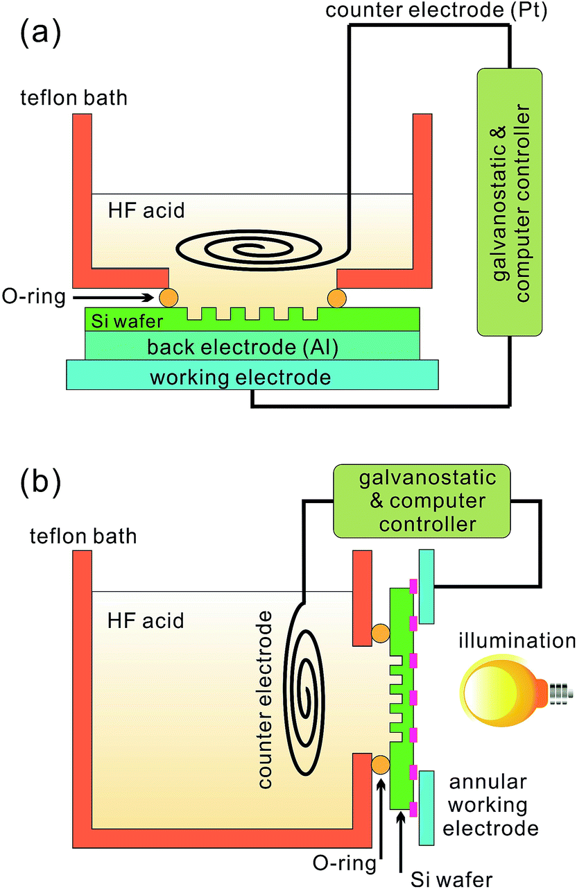 | ||
| Fig. 1 Typical experimental setups for electrochemical HF etching of: (a) p-Si; and (b) n-Si.55,56 | ||
Applying a voltage bias or current initializes the etching reaction. According to the current density, the etching can be classified into three regions.57,58 In the low current density region, the etching reaction is limited by silicon oxidation, leading to the formation of porous silicon. In the high current density region, a large number of holes are injected into the bulk material and diffuse over the entire surface of the wafer. In this case, the etching reaction is limited by the removal of the oxide; consequently, the wafer becomes electrochemically polished. Between these two regions, there exists a transition region, where randomly distributed nano-pillars can be produced without using a mask.59 The exact current density values defining these three regions depend on the doping types and concentrations of the wafers, [HF], illumination conditions and so forth.60 For a moderately doped p-Si wafer in 1% HF solution in the dark, the maximum current for porous silicon production amounts to ∼3 mA cm−2; electrochemical polishing occurs as the current density exceeds ∼5.5 mA cm−2.58
With a photolithography defined mask, three-dimensional micro- and nano-structures can be fabricated, during which only selected areas are electrochemically polished.55,59,61 For the sake of BSi, however, our subsequent discussion will only focus on the low current region.
The etching reaction in the low current region is mainly controlled by adjusting the current density, [HF], etching time and illumination. The resulting silicon pore sizes increase as the current density rises, or as [HF] drops. The pore depths propagate as etching time increases. When moderately doped n-Si is used, illumination is often employed, since hole generation is a limiting factor during the etching of this type of wafer in the dark (Fig. 1b).
The resulting pore morphologies also depend on the wafer doping type and dopant concentration. Put simply, for p-Si, the pore size increases with doping concentration, from 1 to 100 nm; for n-Si, it decreases with doping concentration, from 10 μm to 10 nm.58
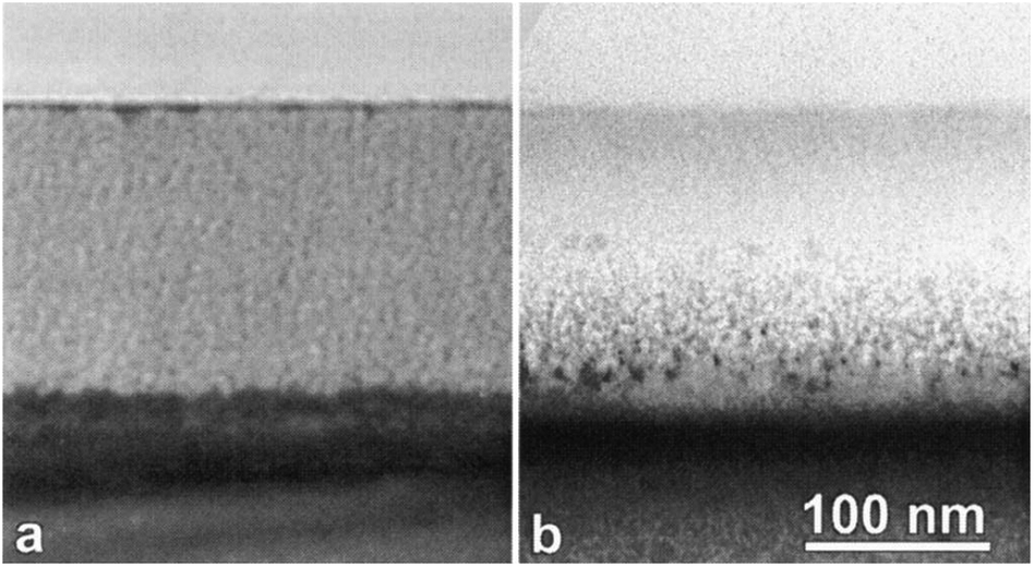
For most typical laboratory-based synthesis methods, the most convenient and flexible control parameters during electrochemical etching are current density and etching time. By applying a constant current, the porosity of a silicon wafer remains the same as its pores grow into the substrate (Fig. 2a). In contrast, changing current density and its related time profile can create structures with gradual variations or step changes in its porosity and refractive index. For example, Striemer and Fauchet continuously varied the etching current during their electrochemical etching from 100 mA to 0 mA over 10 s, and produced a gradual change of porosity from ∼99% to ∼33% (Fig. 3). Their porous layer demonstrated better optical performance than the homogeneous porous silicon film, with a weighted reflectance of only 3.7% at a thickness of 107 nm (Fig. 4).62 In contrast, the homogenous porous silicon often requires a thickness of several μm to achieve the same level of reflectance. A thick porous layer, however, is incompatible with a thin film solar cell bearing a junction depth of only ∼350 nm,62 since this layer itself may absorb, and thence waste, a substantial amount of light.
 | ||
| Fig. 2 TEM images of (a) electrochemically and (b) stain etched porous silicon, with a thickness of ∼150 nm. The porosity is uniform in the electrochemical case, but possesses a gradual transition in the stain etched case.63 Reproduced by permission of the Electrochemical Society. | ||
 | ||
| Fig. 3 SEM image of a gradient index porous silicon, with a thickness of ∼100 nm. Reproduced with permission from ref. 62. Copyright 2002, AIP Publishing LLC. | ||
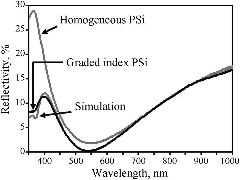 | ||
| Fig. 4 Reflectance spectra of a homogenous porous silicon layer (80 nm thick, 75% porosity) and a gradient index porous silicon layer (100 nm thick). The later spectrum has an excellent match to the simulated reflectance of a porous layer with porosity gradient from 94% to 33%. Reproduced with permission from ref. 62. Copyright 2002, AIP Publishing LLC. | ||
By employing a similar strategy, Ma and co-workers used electrochemical etching to form a multi-layer porous silicon structure with gradual change of porosity and refractive index from air to silicon bulk, with a total thickness of 4.1 μm.64 The resulting structure effectively suppresses the light reflectance to less than 5% in both the visible and IR regions (from ∼350 nm to ∼3.3 μm). Ariza-Flores et al. fabricated 235 nm-thick porous silicon with a gradual porosity change from 92% to 38%, leading to a low weighted average reflectance of 1.3% from 300 to 1100 nm.65 By considering only the solar spectrum region, Osorio et al. also designed a three-layer porous silicon structure with porosity at 89%, 70% and 41% possessing a corresponding thickness of 75 nm, 56 nm and 39 nm, respectively.66 Its theoretical optical transmittance of 95.7% has been experimentally verified.66 Note that Osorio et al. took into account light absorption in the porous layer and optimized their structure based on the maximum optical transmittance, instead of the minimal reflectance.
Multi-layer porous silicon is composed of layers with different refractive indices. Interference within these layers can be used to create selective reflectance or transmission by making use of the antireflection and the Bragg effects.67 Consequently, the etched silicon wafers exhibit different colors under white illumination (Fig. 5).68 Similarly, the reflection properties of the multi-layer structure, the so-called super-lattice, can be altered for a wide range of photonic and optical devices, such as a distributed Bragg reflector,10,11 Fabry–Perot interference filter,12 micro-cavity,13,14 and Rugate filters.15
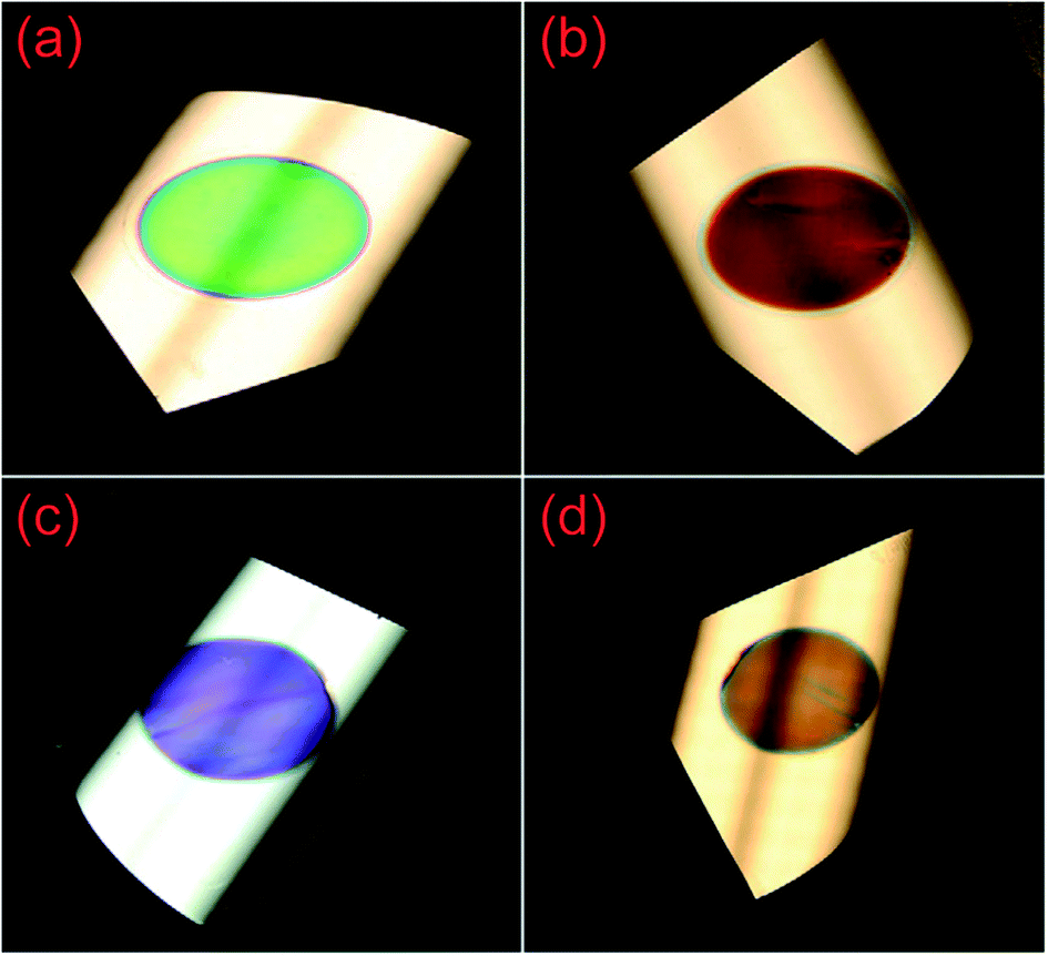 | ||
| Fig. 5 Multi-layer porous silicon samples under the illumination of a white fluorescent lamp, exhibiting different colors: (a) green; (b) red; (c) purple; and (d) orange. Only a circular area of ∼4 cm2 has been electrochemically etched for each wafer and displays different colors, while the untreated area reflects white light.68 Adapted by permission of Elsevier. | ||
Electrochemical HF etching is low cost, easy to implement, compatible with standard microelectronic fabrication techniques, and allows the creation of porous silicon with a wide range of structures and applications. It can be applied to both crystalline silicon (c-Si) and multicrystalline silicon (mc-Si).63 While it has been a concern to apply this technique to handle large surface areas, such as are in demand for industrial applications, owing to the required high current,69 Semiconductor Systems Corporation (SEMSYSCO) has introduced a semi-automated pilot line (SEMSYSCO PoSi), which is able to handle up to 216 wafers per run.70 Nevertheless, maintaining a uniform current density over a large surface area is likely to be a challenging task for applying electrochemical HF etching to a large-scale industry process.
2.2. Stain etching
Stain etching employs HF and HNO3 to perform chemical etching of silicon, leading to the formation of porous silicon.71 H2O and/or acetic acid are often added to dilute [HF] and [HNO3], while acetic acid also acts as a wetting agent. The etching action of HF–HNO3 is based on a successive oxidation-followed-by-dissolution process, in which HNO3 is responsible for injecting holes and oxidizing silicon, and HF for removing the oxide formed.72By controlling the concentration ratio of HF and HNO3, or C = [HF]/[HNO3], different silicon surface morphologies can be formed.73–76 In short, when [HF] is high and [HNO3] is low, the etching rate is determined by the oxidization rate, and porous silicon is formed in this region for both n- and p-Si.49,77 In contrast, when [HNO3] far exceeds [HF], the etching reaction is limited by the removal of silicon oxide via HF. In this high [HNO3] region, HF–HNO3 is often used for silicon surface cleaning and damage removal, or surface polishing.39,78,79 By properly adjusting C, one may also texturize mc-Si, when conventional alkaline chemical etching is not suitable, due to its anisotropic nature and the diverse crystal orientations on a mc-Si wafer.80 Owing to its similarity to electrochemical HF etching (Section 2.1), stain etching is often considered as a localized electrochemical etching process. It bears some similarity to metal-catalyzed chemical etching methods (Section 2.3), since HNO3 reduction is autocatalytic, due to the formation of an intermediate compound, HNO2.81
However, in contrast to the other two techniques, stain etching also removes the top surface of silicon at a relatively high rate. This effect impacts in two ways. First, it produces a gradual transition in porosity, i.e., from silicon bulk to 100% porosity (Fig. 2b).41 Second, there is an upper limit for the thickness of the porous layer produced by stain etching.77 This is because the pore propagation rate drops as the porous silicon layer becomes thicker, due to the lower diffusion rate of reactants and reaction products within the deep pores. When this rate matches the etching rate at the top surface of the porous layer, the maximum thickness of the porous layer is achieved.82 While the exact value of this maximum thickness varies according to experimental conditions, 300–400 nm has been reported for p-Si77 with a boron doping concentration of 2 × 10¹⁵ atom per cm3. This maximum thickness, however, increases in line with the silicon doping concentration.77 For example, 700–800 nm has been reported for a boron doping concentration of 2 × 10¹⁶ atom per cm3, and infinite for 1018 atom per cm3. This phenomenon can be explained by the presence of a higher number of active structural defects in highly doped silicon, which can easily be attacked by the etchant and thus boost the rate at which pores propagate.
Another important control parameter of stain etching is represented by C × t, where C = [HF]/[HNO3] and t is the etching time. Since stain etching works in the low [HNO3] region and HNO3 is a reaction limiting factor, increasing [HNO3] scales up the etching rate. Similarly, extending the etching time affords a thicker porous layer (when the film thickness is less than the maximum achievable thickness). Consequently, a constant C × t leads to the formation of a porous silicon layer with an approximately fixed layer thickness; the reflectance of the porous silicon drops, when C × t increases.41 Nevertheless, varying t changes the wavelength at which the reflectance is at the minimum (Fig. 6);63 and changing C has a greater impact on the absolute reflectance value. By tuning these two parameters, one can adjust the effective refractive index of the porous layer from 1.5 to 2.2.41
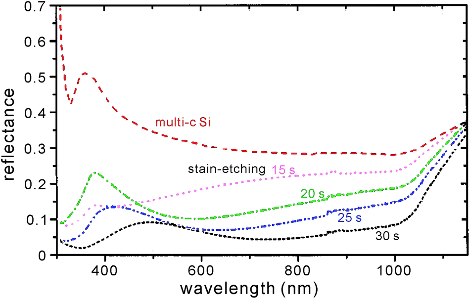 | ||
| Fig. 6 Reflectance spectra of stain etched porous silicon on a mc-Si wafer. The reflectance over the entire VIS-NIR band is lowered, as the etching time, t, increases and the porous layer becomes thicker. The AM1.5 weighted reflectance from 300–1000 nm amounts to 32.0% (0 s), 18.9% (15 s), 13.6% (20 s), 9.7% (25 s), and 6.3% (30 s), respectively; the corresponding porous layer thickness is ∼100 nm (15 s) and ∼150 nm (30 s), respectively.63 Reproduced by permission of the Electrochemical Society. | ||
A modified version of stain etching was introduced by Bessais et al.83–89 Instead of performing the etching in the solution phase, they used HF and HNO3 vapors. It was found that a luminescent white powder made of (NH4)2SiF6 is produced when the HF–HNO3 gas volume ratio is between 2![[thin space (1/6-em)]](https://www.rsc.org/images/entities/char_2009.gif) :1 and 4:1. As this ratio rises above 9:1, porous silicon is formed.87 The resulting structure forms interconnected clusters, containing dot-like silicon particles. In this case, pore propagation is perpendicular to the substrate surface. This feature is similar to that of electrochemical etching, but in contrast to stain etching, which affords curved pore propagation.83–85 Moreover, the reaction rate of chemical vapor etching is much lower than that of stain etching, causing less damage to other materials, such as metal lines, deposited on the silicon surface. This technique also allows the fabrication of much thicker porous layers, (>100 μm).86
:1 and 4:1. As this ratio rises above 9:1, porous silicon is formed.87 The resulting structure forms interconnected clusters, containing dot-like silicon particles. In this case, pore propagation is perpendicular to the substrate surface. This feature is similar to that of electrochemical etching, but in contrast to stain etching, which affords curved pore propagation.83–85 Moreover, the reaction rate of chemical vapor etching is much lower than that of stain etching, causing less damage to other materials, such as metal lines, deposited on the silicon surface. This technique also allows the fabrication of much thicker porous layers, (>100 μm).86
Stain etching is an economic and facile route for scaling up, owing to its wet process character. It is also fast and able to suppress silicon reflectance to below 10% within a short time frame (on the order of 10 s).63 The resulting surface nanostructures display strong luminescence due to quantum confinement, and can be used for optoelectronic applications.49,90 Stain etching also works well on c-Si and mc-Si, and is only slightly grain-dependent.63 However, it offers less control compared with other techniques, and is not suitable where very thick porous layers are desired. As a result, this technique remains relatively unpopular.
2.3. Metal-assisted chemical etching
Silicon can be etched in the presence of HF and an oxidative agent, catalyzed by noble metals, to form micro-/nano-structured surfaces with various morphologies.91 This technique has been thoroughly reviewed by Huang et al. in 2011.92 Here, we briefly summarize its mechanism and interest from the solar cell perspective, and review recent developments.In a typical etching process, a silicon substrate is partly covered by noble metal nanoparticles, and immersed in a solution of HF and an oxidative agent.92–94 For noble metals, gold (Au) and silver (Ag) are the two most popular candidates since they can be deposited onto the surface under vacuum (i.e., via thermal evaporation, sputtering and electron beam evaporation) or in solution (i.e., via electroless deposition and electrodeposition).92,94 Vacuum deposition offers a higher degree of control over the metal film morphology, while electroless deposition affords a simpler process and can be adopted when the requirement on silicon surface morphologies is less stringent.92 Our subsequent discussion will mainly be based on electroless Au or Ag deposition.
During deposition, a compound containing Au or Ag ions, such as AgNO3 or HAuCl4, is added to a HF–H2O2 solution. Upon attachment to the silicon substrate, noble metal ions acquire electrons from the silicon valence band and are reduced to form seed nuclei which develop into nanoparticles. Concurrently, these ions inject holes underneath the silicon causing oxidation into SiO or SiO2, which are then removed by HF.92 By the continuous formation of silicon oxide underneath the metal particles and the corresponding removal action by the HF, the metal particles sink into the silicon and create porous structures (Fig. 7).92 The depth of these pores is proportional to the etching time.95 Once the desired surface structures are created, the metal nanoparticles are removed by another etchant, such as HNO3, followed by a cleaning process.
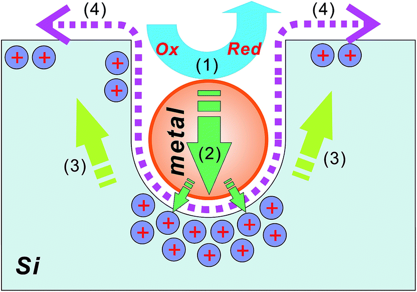 | ||
| Fig. 7 An illustration of the metal-assisted chemical etch process: (1) the reduction of an oxidative agent (such as H2O2) catalyzed by a noble metal particle; (2) the injection of the holes generated during the reduction reaction, into the silicon substrate, with the highest hole concentration underneath the metal particle; (3) the migration of holes to silicon sidewalls and surfaces; and (4) the removal of oxidized silicon via HF.92 | ||
Metal catalysis plays a key role during the chemical etching process. Koynov et al. showed that without metal catalysis, the etching speed was very low (∼1 nm min−1). In contrast, this speed was greatly increased by the addition of Au; ∼250 nm high-hillock structures were fabricated within 50–90 s.96 Consequently, the size and shape of deposited metal particles largely determine the morphologies of the etched surface, since the silicon underneath this metal catalyst is etched much faster. By varying the surface coverage and distance between metal particles, one can create a wide range of surface nanostructures, from BSi layers to nanowires.96,97
Several strategies can be employed to produce more sophisticated structures using metal-assisted chemical etching. For example, the etching can be performed via a two-step process.98 During the first step, highly dispersed silver nanoparticles are deposited onto silicon, followed by a long etching step to form deep pores. In the second step, more concentrated silver nanoparticles are employed for a quicker etching in order to increase the porosity in the topmost layer. This two-step process leads to a smoother transition of porosity (and the corresponding refractive index) from air to bulk silicon, affording a lower reflectance compared with single-step etching.98
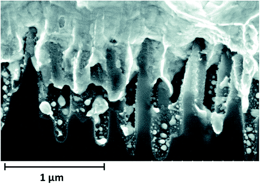
Another strategy to produce gradient refractive indices is to use reactive ion etching (RIE; see Section 2.4) to retouch the nanostructures produced by metal assisted chemical etching. For example, the nanostructures fabricated via Ag catalyzed chemical etching are usually columnar, with near vertical side walls and blunt tips [Fig. 8a and b].99 By applying RIE to such structures, needle-like structures can be created [Fig. 8c and d], leading to very good anti-reflection results (Fig. 9). Li and co-workers coated silicon wafers with such structures (7.1 μm in height and 50–150 nm in diameter) causing its reflectance to decrease to less than 2% from 250–1000 nm (Fig. 9).99
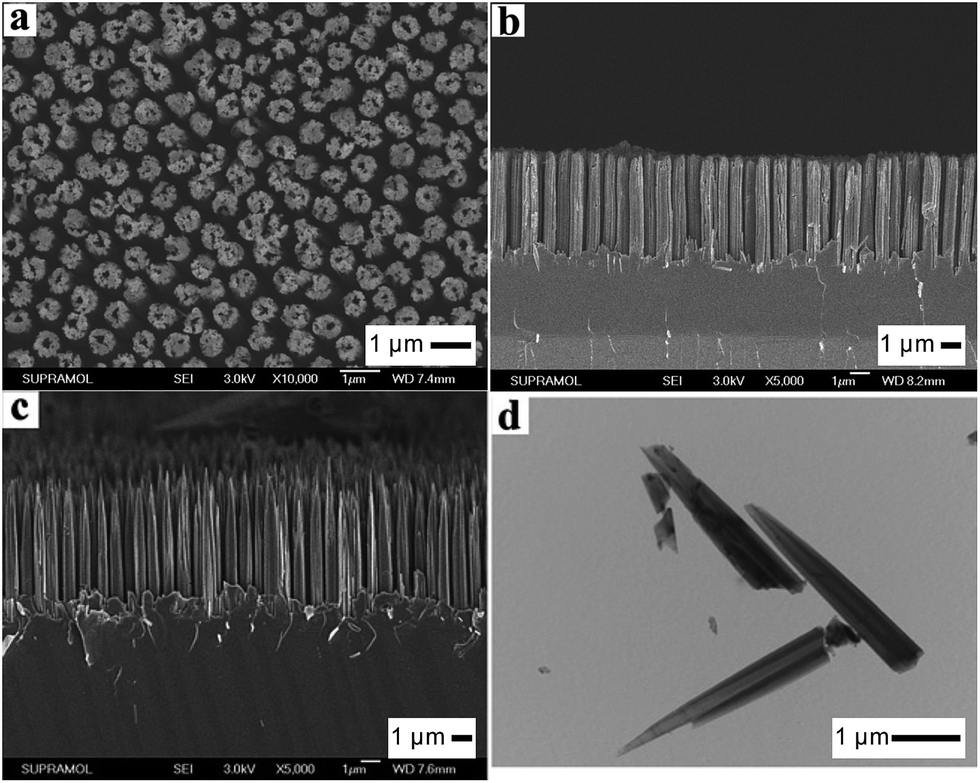 | ||
| Fig. 8 SEM images of (a) top view and (b) side view of a hollow silicon columnar array, formed via Ag-assisted chemical etching; and (c) side view of this array after a quick RIE process, demonstrating hollow needle-like structures, with a height of ∼7.1 μm; (d) TEM image of the hollow-needles isolated from the silicon substrate.99 Reproduced by permission of the Royal Society of Chemistry. | ||
 | ||
| Fig. 9 Reflectance spectrum of hollow-needle arrays of different lengths, i.e., 2.1 μm (black solid line), 3.4 μm (gray solid line), and 7.1 μm (black dash line) in the UV-VIS-NIR region.99 Reproduced by permission of the Royal Society of Chemistry. | ||
Furthermore, densely-packed periodic nanostructures can be obtained by applying a mask, which may be defined by interference lithography,100 colloidal particle deposition,99 or phase segregation of block-copolymers.101
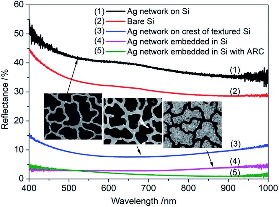
Although metal removal is often performed after the nanostructure formation, it is not always necessary. Recent work by Guo et al. made use of the deposited metal to produce a conductive BSi surface.102 In that work, a dual layer of indium (In) and SiOx was deposited onto a silicon wafer. The deposited In forms islands and the gap between such islands is enlarged via HNO3 etching when necessary (from tens to more than 100 nm, or 80 nm in the reported case). Using these islands as a mask, Ag was deposited via a lift-off process, forming an Ag mesh, instead of individual nanoparticles (Fig. 10). As the Ag catalyzed chemical etching proceeds, the Ag mesh sinks into silicon substrate, in parallel to the nanostructure formation. The resulting structure has a very low reflectance over a broadband (Fig. 11). The weighted reflectance (from 400 to 1000 nm) without any additional antireflection coating was measured at 3.2% and 8.0%, at nanostructure depths of 600 and 200 nm, respectively.102 In particular, the embedded Ag network effectively minimizes metal shading effects and contributes to the improved reflectance, unlike other exposed metal contacts. While making good contact on nanostructures has been a challenging task, good electrical conductivity (∼7 Ω □−1) has been achieved with an embedded Ag network.102 Nevertheless, this structural design also introduces an enlarged Si/Ag interface; and the resulting carrier recombination is expected to be high.
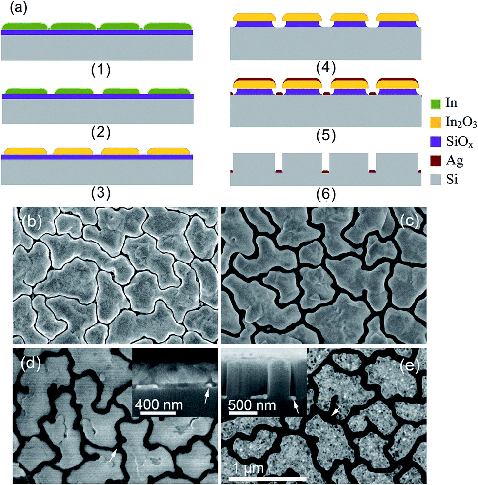 | ||
| Fig. 10 (a) Schematic illustration of Guo's experimental procedures to fabricate conductive BSi surfaces: (1) deposition of a dual layer (In/SiOx) thin film on a silicon wafer; (2) enlargement of the gap size between In islands via dilute HNO3 etching; (3) oxidation of In islands; (4) HF etching through an In2O3 mask; (5) deposition of Ag film, to form an Ag nanowire mesh on a silicon substrate; (6) Ag-assisted chemical etching, during which the Ag mesh sinks into the silicon wafer and the In2O3 mask is removed. (b)–(e): SEM images corresponding to fabrication steps (1), (2), (5) and (6). In (d) and (e), the Ag nanowire meshes are indicated by arrows.102 Reproduced by permission of John Wiley & Sons, Inc. | ||
 | ||
| Fig. 11 Reflectance spectra of different BSi samples.102 Reproduced by permission of John Wiley & Sons, Inc. | ||
In summary, metal-assisted chemical etching is a simple, fast, low cost and versatile process for fabricating a wide range of nanostructures with minimal hardware requirements. The morphologies of the resulting silicon surfaces can be controlled by varying the process parameters, such as the size, shape and surface coverage of noble metal nanoparticles, etchant concentration and the etching time.103 This etching technique can be applied to c-Si, mc-Si, and amorphous Si (a-Si),104,105 as well as other materials, such as GaAs, GaN, and SiC.92 It has grown increasingly popular over the last decade, especially in a research context, and remains as a mainstream etching method. From a solar cell perspective, however, metal contamination is a major concern with this technique, and a thorough metal removal and cleaning process is required to address this problem.
2.4. Reactive ion etching
The use of reactive ion etching (RIE) to form grass-like BSi surfaces was first reported by Jansen et al. in 1995.106,107 This method employs SF6 and O2 gases to generate F* and O* radicals. F* is responsible for etching silicon, producing volatile products such as SiFx. These products, particularly SiF4, react with O* to form a passivation layer of SiOxFy on a cooled silicon substrate.108,109 This passivation layer is partly removed by ion bombardment and the exposed silicon is further etched by F*. The etching reaction is exothermic, and reduces the chance of producing a new passivation layer since SiOxFy is prone to desorption upon heating. In contrast, there is far less ion bombardment on the side walls of the formed silicon columns; so the passivation layer there is largely preserved, preventing further etching.110 This etching/passivation competition mechanism leads to the formation of random silicon microstructures with very high aspect ratios in a self-masking fashion (Fig. 12). | ||
| Fig. 12 SEM images of BSi fabricated by RIE under different conditions. (a) and (b) Top and side views of BSi, with RF power = 1500 W, bias = 40 V, O2/SF6 = 0.09, pressure = 10 Pa, time = 10 min. (c) and (d) top and side views of BSi, with RF power = 1500 W, bias = 30 V, O2/SF6 = 0.07, pressure = 3 Pa, time = 30 min.110 © IOP Publishing. Reproduced by permission of IOP Publishing. All rights reserved. | ||
The morphology of the BSi made in this manner can be adjusted by changing various RIE parameters, such as gas composition and flow rate, system temperature, substrate bias and RF power.111–115 By increasing the O2 flow rate, deposition of the passivation layer is enhanced. Raising the temperature increases the desorption rate of the passivation layer; in fact, SiOxFy mostly desorbs as the wafer temperature is raised from −100 °C to −60 °C;113 this effect also indicates that RIE is typically performed at low temperature, i.e., at −110 °C, and is sometimes referred to as cryogenic RIE in the literature. By tuning the coverage of the passivation layer, one gains control of the nanostructure density. Moreover, increasing substrate bias during the RIE process controls the kinetic energy of the ions and the associated ion bombardment effects, thus determining the etching rate.
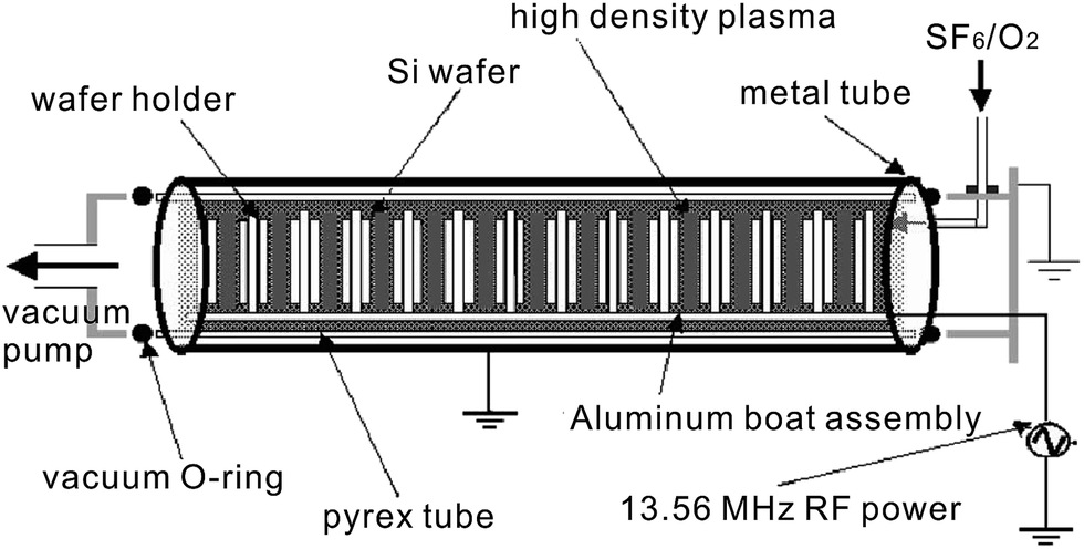
In addition to conventional RIE systems, a number of improved experimental setups have been introduced. Yoo et al. designed a multi-cathode RIE setup,116 making use of the hollow cathode effect (Fig. 13).117 In this system, a number of cathodes are placed in parallel, allowing multiple wafers to be processed simultaneously. As the parallel-oriented cathodes are negatively biased, electrons are trapped between the electrode plates and produce a high density plasma, approximately one order of magnitude greater than that generated by a standard parallel plate RIE system. Owing to the high plasma density, the etch rate is greatly enhanced. Moreover, this system is also characterized by its low voltage, which ensures less ion-induced wafer damage. Using this system, Yoo and co-workers successfully fabricated “needles” of BSi with diameters of 50–100 nm and heights of ∼500 nm. The reflectance of the resulting BSi was close to zero, over the wavelength range from 200 to 1100 nm.116
 | ||
| Fig. 13 A multi-cathode RF system for RIE process.116 Adapted by permission of Elsevier. | ||
Xia and co-workers employed plasma immersion ion implantation (PIII) to perform SF6/O2 reactions with silicon substrates.118,119 In the PIII setup, a strong negative bias (∼−500 V) is applied to the wafer holder, which is immersed in a plasma cloud. This negative bias repels electrons from the holder, but attracts and accelerates positive ions to the wafer for doping, surface modification, sub-surface chemical reaction and so forth.120 It affords simpler machine design and maintenance for large-area and high-throughput processing with a uniform dose.120 By varying the SF6/O2 gas composition, a wide range of surface structures have been fabricated (Fig. 14) that exhibit a broadband of low reflectance, with weighted value (from 200–1100 nm) down to ∼1% (Fig. 15).
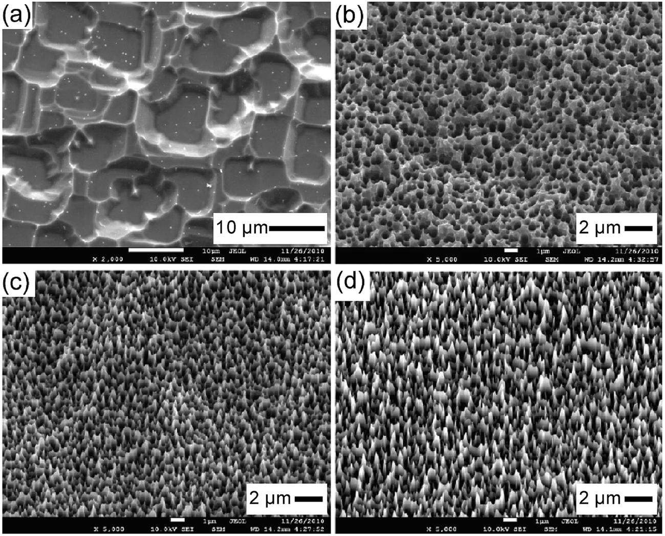 | ||
| Fig. 14 SEM images of BSi samples fabricated via the PIII process at different reactive gas flow rates. (a) SF6; (b) SF6/O2 = 3.5; (c) SF6/O2 = 4.0; and (d) SF6/O2 = 4.5.118 Reproduced by permission of Elsevier. | ||
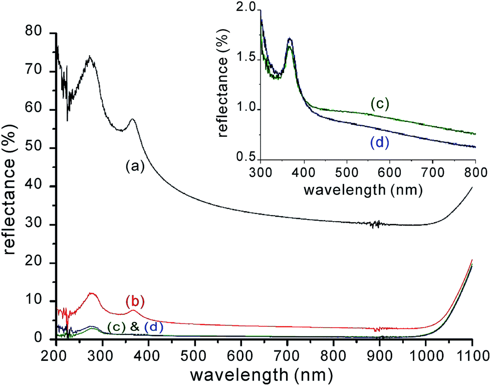 | ||
| Fig. 15 Reflectance spectra of BSi samples produced by PIII etching, as a function of SF6/O2 gas ratio: (a) SF6 (black); (b) 3.5 (red); (c) 4.0 (green); and (d) 4.5 (blue). The inset shows magnified spectra of cases (c) and (d).118 Adapted by permission of Elsevier. | ||
It is also possible to replace or change the composition of the reaction gases, SF6/O2, which are constrained by a tight composition window to achieve an optimal BSi texture. For example, Murias et al. added CH4 into SF6/O2 to enhance the micro-masking effect, due to the formation of polymer on silicon.121 Consequently, their RIE produced a high density of pyramid-like structures in the resulting BSi, with average reflectance down to ∼4% in the 400–700 nm region.
Another alternative reactive gas is Cl2,122–125 which offers a lower etching rate in comparison to SF6/O2 but is much easier to manage, owing to the formation of nonvolatile by-products, and thus makes the control over the passivation layer deposition and silicon etching comparatively straightforward.122–124 Cl2 can also be added into SF6/O2 to enlarge the gas composition working window. Lee et al. claimed that in this new system, the in situ surface damage removal could be realized by properly adjusting the plasma power density and gas composition.126
Several other groups have used SiH4, CH4, Ar and H2 as reactive gases to fabricate sharp grass-like silicon tip structures during high-density electron cyclotron resonance plasma etching.127–129 In these experiments, the reaction of SiH4 and CH4 forms nano-sized SiC which acts as a silicon mask, leaving the uncovered silicon substrate to be etched by argon and hydrogen plasma. The morphologies of the resulting structures can be easily controlled by adjusting system temperature, gas pressure and composition. Increasing the temperature raises the SiC mask formation rate, and boosts the desorption of reactive ions, such as H, H+, H2+, H3+, Ar+, Ar2+, ArH+, thus limiting the etching rate. Consequently, the coverage of SiC increases, while the density and length of resulting nanostructures decrease. At a very high temperature, the SiC formation rate becomes so high that the resulting SiC nano-clusters cover the entire wafer surface, preventing further etching.127,128 Using this approach, Huang et al. fabricated tapered aperiodic structures with apex diameters of ∼3–5 nm, base diameters of ∼200 nm, and lengths from 1 to 16 μm (Fig. 16). These structures effectively suppress reflection over a broad wavelength range, and across a wide range of incidence angles and for both s- and p-polarized light (Fig. 17). The anti-reflection result improves as the silicon surface structures increase in height. For a heights above 5 μm, the reflectance is below 1% over 0.5–2.5 μm, and as low as 0.2% in the 250–400 nm range.129
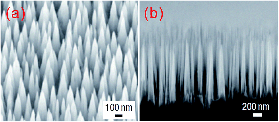 | ||
| Fig. 16 SEM images of (a) a tilted top view and (b) a side view of a silicon nano-tip array, with a base diameter of ∼200 nm and a height of 1600 nm.129 Reproduced by permission of Nature Publishing Group. | ||
 | ||
| Fig. 17 Reflectance spectra of a planar silicon wafer (solid line, black), and Si nano-tip arrays with different heights, i.e., 1.6 μm (green), 5.5 μm (blue) and 16 μm (red) in the UV-VIS-NIR region.129 Reproduced by permission of Nature Publishing Group. | ||
Similarly, Chen and co-workers have employed hydrogen bromide (HBr) and oxygen (O2) during their plasma enhanced RIE.130 During this process, bromide ions are primarily responsible for etching silicon, resulting in the formation of SiBr4. This reaction product can also react with O* radicals to form random distributed SiBrxOy particles, acting as etching masks. By adjusting the gas flow ratios (as well as other process parameters, such as substrate temperature) and controlling this etching-passivation competition mechanism, a wide range of nanostructures, such as nanowhiskers, nanorods and nanotips, have been fabricated.130
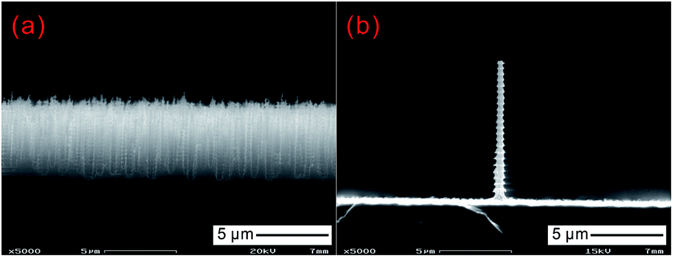
It is also worth mentioning another deep RIE, or Bosch, process, in which CF6 and C4F8 are alternatively introduced into the reaction chamber for etching and passivation, respectively.131,132 By repeating this process for hundreds or even thousands of cycles, a very deep and near-vertical silicon needle structure can be fabricated (Fig. 18). Note that this two-step cycle process induces an undulating structure on the sidewalls of the silicon needles, with an amplitude of several hundreds of nanometers, in contrast to the smooth side wall produced by cryogenic RIE (Fig. 12).
 | ||
| Fig. 18 (a) SEM image of BSi formed by Bosch RIE process; (b) SEM image of a single silicon “needle” produced by Bosch RIE process, with undulated side wall. Image Courtesy of Christoph Kubasch from Institute of Semiconductors and Microsystems, Faculty of Electrical and Computer Engineering, Dresden University of Technology. | ||
RIE can also be performed in combination with photolithography or colloidal-particle defined masks to produce periodic or quasi-periodic structures.133,134 RIE systems are commercially available and are able to process various types of silicon wafers on a large scale. However, its process optimization is relatively complicated, and its cost is also potentially high, owing to the use of vacuum equipment.135 Moreover, RIE causes significant surface damage to the silicon substrate, reducing the minority carrier lifetime near the surface region (Fig. 19).136,137 In order to recover the minority carrier lifetime, a subsequent etching is required to remove the top 20–50 nm of the wafer surface, in addition to a RCA (Radio Corporation of America) cleaning of the sample that removes the metallic and organic contaminants. Additional measures, such as lowering the RF power and substrate bias, limiting the process time and usage of O2 during RIE etching, and performing wafer annealing at high temperature (i.e., 400 °C) after the etching, also help to improve the minority carrier lifetime, but at the expense of a lower etching or throughput rate and higher cost.136
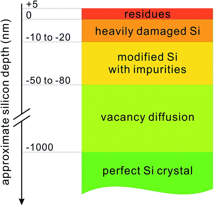 | ||
| Fig. 19 A schematic illustration of the RIE induced damage to a silicon substrate.136 | ||
2.5. Laser treatment
Femtosecond-laser (fs-laser) treatment is a versatile technique for performing surface texturing on silicon substrates.138–144 By irradiating a silicon wafer with a fs-laser in SF6, Mazur et al. produced conical silicon spikes up to 50 μm high, with a base area of ∼6 × 10 μm2, tapering to ∼1 μm at the tip. The fs-laser structured silicon micro-spike consists of a crystalline core, a highly disordered surface layer (<1 μm thick), and is covered with silicon nanoparticles of 10–50 nm in diameter [Fig. 20a, c and e].142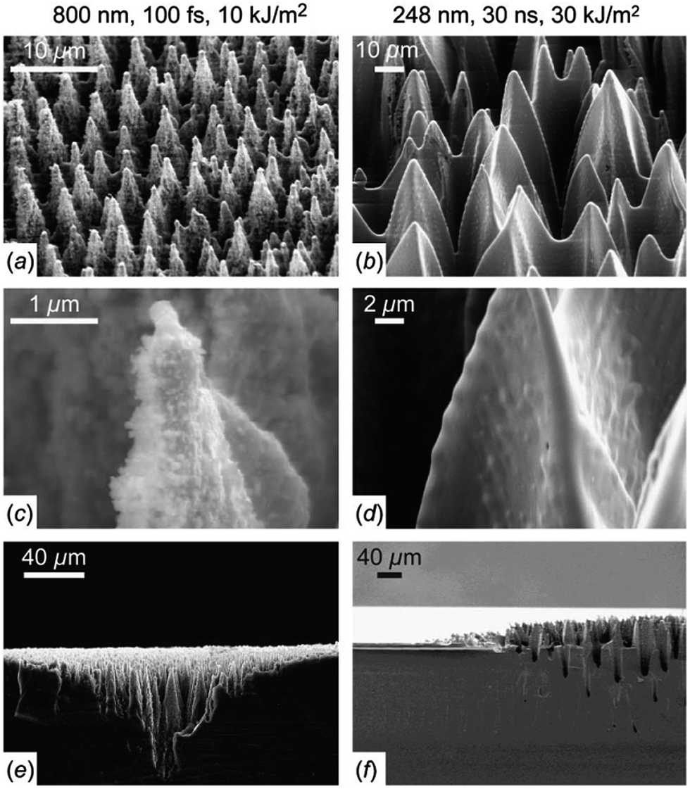 | ||
| Fig. 20 SEM images of laser-treated silicon surfaces in a SF6 environment with [(a), (c) and (e)] fs-laser, and [(b), (d) and (e)] ns-laser. (e) and (f) show the side views of the snapped samples. Reproduced with permission from ref. 142. Copyright 2004, AIP Publishing LLC. | ||
In these experiments, since the laser pulse is in the sub-picosecond region, thermal equilibrium cannot be established in the silicon substrate. Instead, the excitation of electrons from the bonding to anti-bonding states causes repulsive forces and disorder in the lattice structure while remaining thermally cold.145 Both experiments and simulation have showed that the covalently bonded lattice becomes unstable and leads to disorder formation upon the excitation of ∼10% electrons from the valance band to the conduction band; this mechanism is responsible for the roughened silicon surface.
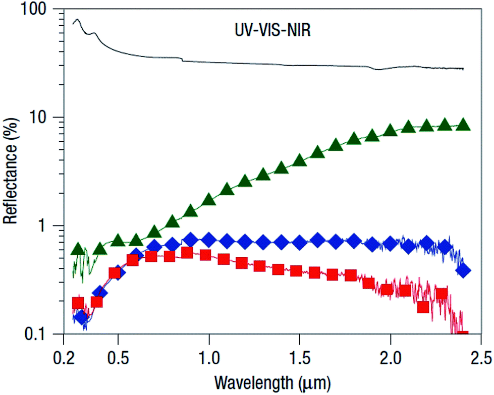
While the roughened surface texture here greatly minimizes surface reflection, one major advantage of laser treatment in a SF6 environment is the introduction of sulfur atoms (∼1 atom %) and structural defects into the silicon lattice of the final product, thus creating more absorbing states in the sub-band gap region of silicon.141,146 These two factors result in ∼90% absorption efficiency from 0.25 to 2.5 μm for silicon wafers coated with ∼10–12 μm long spikes, compared to an untreated silicon surface, with absorption efficiency of merely ∼60% which occurs mainly in the visible region (Fig. 21). Similarly, selenium and tellurium can also be introduced into silicon by spreading their powders onto a silicon substrate147 or applying ion implantation,148 followed by laser irradiation. Such doping also leads to strong sub-bandgap absorption.147,148 It is interesting to point out that ion-implantation can also be applied to BSi fabricated by other techniques, such as metal-assisted chemical etching, to realize sulfur doping and sub-band absorption.149
 | ||
| Fig. 21 Absorbance spectra of laser treated BSi samples and a standard wafer. Reproduced with permission from ref. 141. Copyright 2001, AIP Publishing LLC. | ||
Owing to laser induced damage, this micro-structured silicon surface is rendered less electronically active.150 Post-annealing is often performed to reduce the number of defects and improve carrier mobility, while leaving the silicon surface morphology largely unchanged.142 However, the annealing temperature requires careful control, because a low temperature anneal does not remove sufficient defects, causing a poor electronic response in the silicon substrate. In contrast, a high temperature annealing significantly decreases the below-bandgap absorption, degrading the overall photoresponse of the micro-structured wafer.146
Where doping is not required, one may perform laser irradiation in vacuo, or in a non-reactive gas environment. In this case, blunted structures are produced.139 For example, Sarnet et al. have produced microstructures with heights of ∼10 μm and spacings of ∼2.5 μm, so-called “penguin” structures, which have much smoother surfaces in comparison to those produced in SF6 (Fig. 22).151,152 The penguin structures display a flat high absorbance (>90%) over a broadband (350–1000 nm) and reduce the weighted reflectance of silicon from over 30% to ∼9%, owing to enhanced light scattering and trapping effects.151
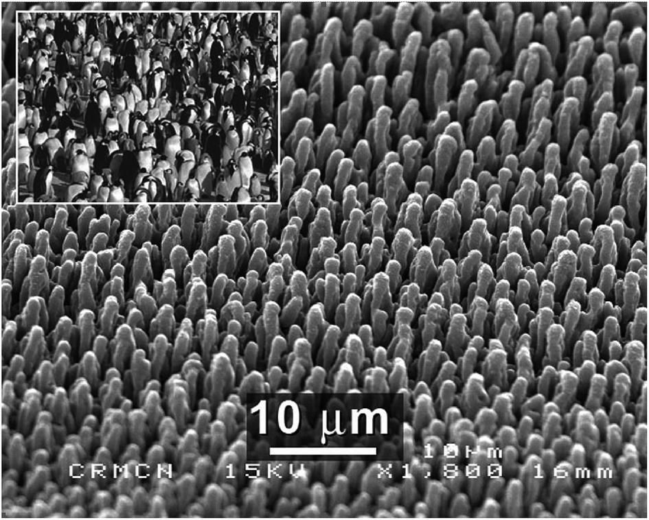 | ||
| Fig. 22 SEM image of penguin-like silicon microstructures created by fs-laser irradiation; the inset shows a real penguin colony.151 Reproduced by permission of Elsevier. | ||
During laser treatment, many parameters can be tuned to optimize the BSi morphology and performance, such as laser polarization, spot size, power density, shot number, scanning parameters, and ambient environment.152–154 Laser power mainly determines the ablation and silicon volatilization rate, and the pulse number controls the interaction time of laser and silicon, since a longer interaction time transfers energy to the deeper part of a wafer.153 Given a certain amount of laser energy, these two factors can be optimized in order to produce very high spikes. In addition, studies by Huang suggest that laser fluence, the energy delivered per unit (or effective) area, plays a critical role on the resulting surface morphology.154 They have shown that as the laser fluence grows, the size of the surface micro- and nano-structures generally increases and the surface roughness is greater. Crucially, the spatial frequency of these features follow a discrete decreasing pattern, i.e., 2f, f, f/2, f/4, and f/8, where f is the fundamental frequency corresponding to near-subwavelength ripples. It is proposed that f/2, f/4, and f/8 are from the 2-order, 4-order, 8-order grating coupling.154 Furthermore, laser treatment can also be performed in water or oil. Much smaller structures, down to sub-100 nm, i.e., one or two orders of magnitude lower than that in the gas environment or in vacuo, have been reported.155,156 These results can be explained by a combined effect of capillary waves on the molten silicon surface in conjunction with laser-induced etching.155 Laser irradiation may also be employed with a periodic mask to produce more ordered micro-spikes on a silicon wafer.157
Laser treatment is not restricted to grain orientation and so can be applied to both c-Si and mc-Si. BSi generated by laser irradiation, especially with sulfur doping, is useful in many different applications. For example, the nanostructured protrusions produced in a SF6 environment are luminescent upon annealing, and the luminescent wavelength can be modified by varying the annealing temperature.150 The improved photo-responsivity of the BSi also makes it an ideal photodiode material (Fig. 23).146,158 Carey et al. have shown that photodiodes made of n-type BSi demonstrate a higher responsivity than commercially available silicon photodiodes, i.e., two orders of magnitude higher in the visible region and five orders of magnitude higher in the near infrared region.146 Moreover, the working window is extended into the infra-red region, owing to the formation of a sulfur-doping induced intermediate band. An avalanche photodiode has also been fabricated with this type of BSi, which offers a lower breakdown voltage (500 V in comparison with 900 V in untextured silicon).141 Heavily sulfur doped silicon can also be used to fabricate intermediate band photovoltaics. Nevertheless, Sullivan et al. have shown that the figure of merit of this material is too low for solar cell applications, in contrast to a single bandgap material.159
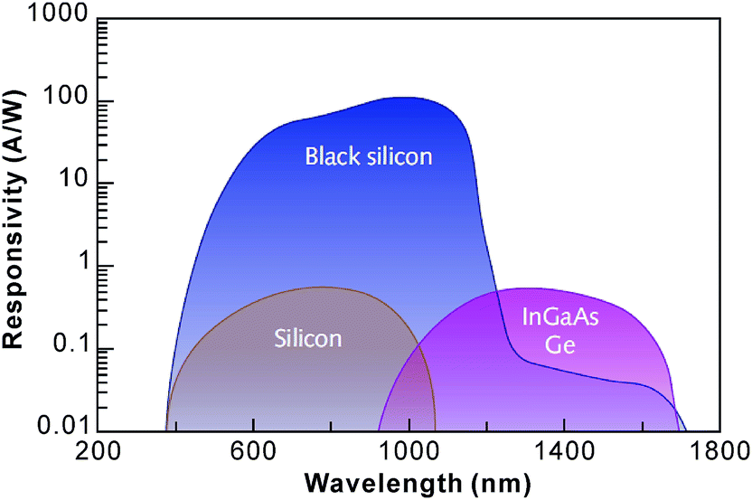 | ||
| Fig. 23 The responsivity of a BSi photo-detector in comparison to those of standard silicon, InGaAs and Ge.160 Reproduced by permission of Laser Focus World. | ||
The laser process is relatively slow in comparison to other etching techniques, especially on an industrial scale, although its processing rate can be improved by increasing laser repetition rate,161 or raising laser power/spot size. Furthermore, laser induced material damage can be quite substantial; thorough defect removal etching is required when a high material quality is of great concern, as in the case of photovoltaic applications.
2.6. FFC-Cambridge process
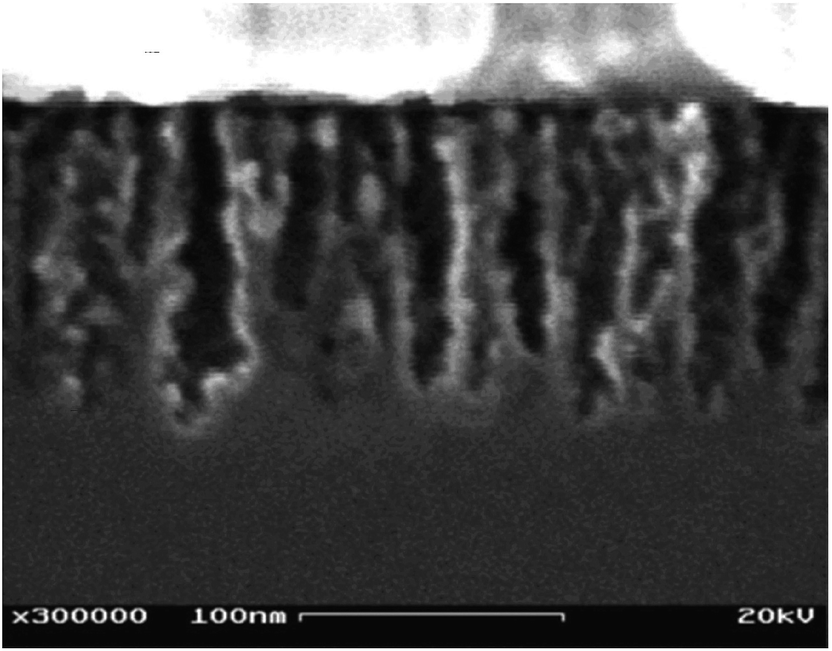
Porous BSi can also be fabricated via the FFC-Cambridge process. This process was first developed by Chen, Farthing and Fray to electrochemically reduce TiO2 to Ti in molten salt CaCl2 at ∼850 °C.162 This simple and cost-competitive approach can also be used to reduce other metal oxides to pure metals, such as Ti, Ta, Cr, and Fe.162 Nohira et al. further extended this method to directly reduce SiO2 to silicon (Fig. 24).163 In Nohira's experiment, a ∼1 mm thick SiO2 plate was bound by Mo wires, forming a cathode, and immersed into molten CaCl2. The surface layer of the SiO2 plate was first reduced into silicon at the conductor (Mo)–insulator (SiO2)–electrolyte (CaCl2) three-phase interface, upon applying a voltage bias (∼−1 V versus Ca2+/Ca) to the cathode. The O2− anions extracted during the process, diffuse through CaCl2, reach the graphite anode, and are then oxidized into mainly O2 as well as some CO and CO2 gases.164 On the cathode side, the reduced silicon is porous, owing to the removal of oxygen from SiO2; the silicon is also conducting at such a high temperature, with a resistivity of ∼0.02 Ω × cm.165 Consequently, the molten salt infiltrates into silicon pores to form a new conductor (Si)–insulator (SiO2)–electrolyte (CaCl2) three-phase interface, which drives the reduction process. Eventually, after electrolysis for one hour, a ∼100–200 μm thick porous silicon layer is produced, with purity higher than 90%.163 The resulting silicon possesses good crystallinity, because the transition from amorphous to crystalline silicon occurs above 470 °C.166,167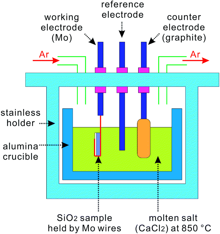 | ||
| Fig. 24 Experimental setup of the FFC-Cambridge process to produce porous silicon.168 | ||
Since Nohira's experiments, the silicon reduction mechanism and process control parameters in the FFC-Cambridge process have been analyzed in detail by several groups.163,164,169–172 The solubility of O2− ions in the molten salt plays a key role in the process,163 where its diffusion in the silicon pores controls the overall SiO2 reduction rate.169 Silicon can be successfully produced when the working electrode (cathode) potential is between −0.70 and −1.25 V (versus Ca2+/Ca), and the reduction rate increases as the cathode potential is lowered. However, when the working electrode potential drops further, i.e., to 0.35 V, the formation of CaSi and CaSi2 alloys becomes quite significant.170 In addition, one may minimize metal contamination during the SiO2 reduction process by replacing the metal electrode with a silicon plate, which can be directly tied to the SiO2 plate. With this strategy, Yasuda et al. obtained a high silicon purity of 99.80% by following the electroreduction with a melting and solidification process at 1500 °C.171
Using the FFC-Cambridge process, the Fray Group successfully produced a layer of porous silicon by electrochemically reducing a 2 μm thick thermal oxide layer.173,174 The porous silicon consisted of globular structures, with diameters of several hundreds of nanometers (Fig. 25). Nano-fibers also exist, with diameters of several tens of nanometers, embedded between these globular structures. The measured reflectance of the porous silicon is ∼10% across the entire silicon absorption spectrum (400–1100 nm; Fig. 26), making it an especially viable candidate for an antireflection coating on silicon solar cells.174 The presence of nano-fibers also suggests that it has potential luminescent applications upon processing and structural optimization.
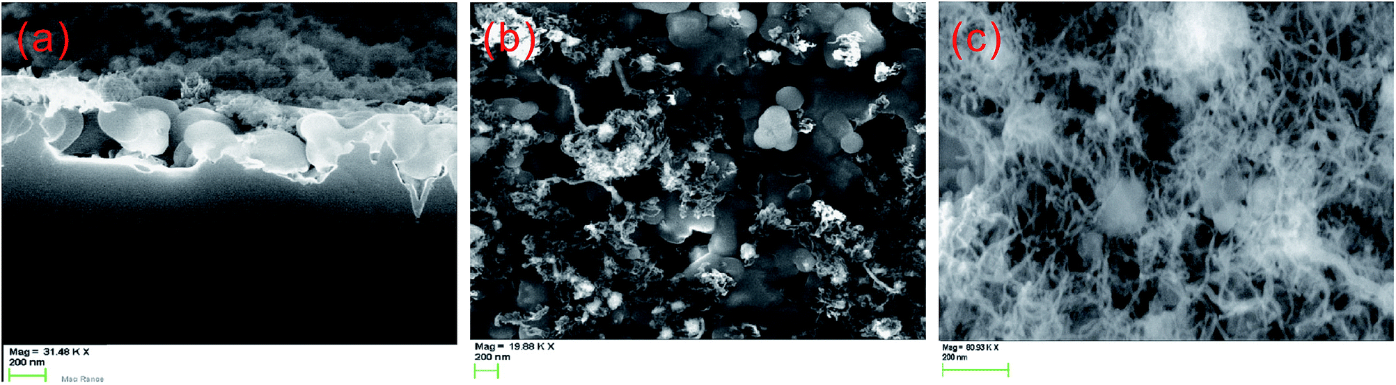 | ||
| Fig. 25 SEM images of porous silicon formed through the FFC-Cambridge process by directly reducing a 2 μm SiO2 precursor at E = −1.0 V and t = 20 min. (a) Side and (b) top views of silicon nano-nucleation; and (c) top view of silicon nano-fibres. Scale bar = 200 nm.174 Reproduced by permission of the Electrochemical Society. | ||
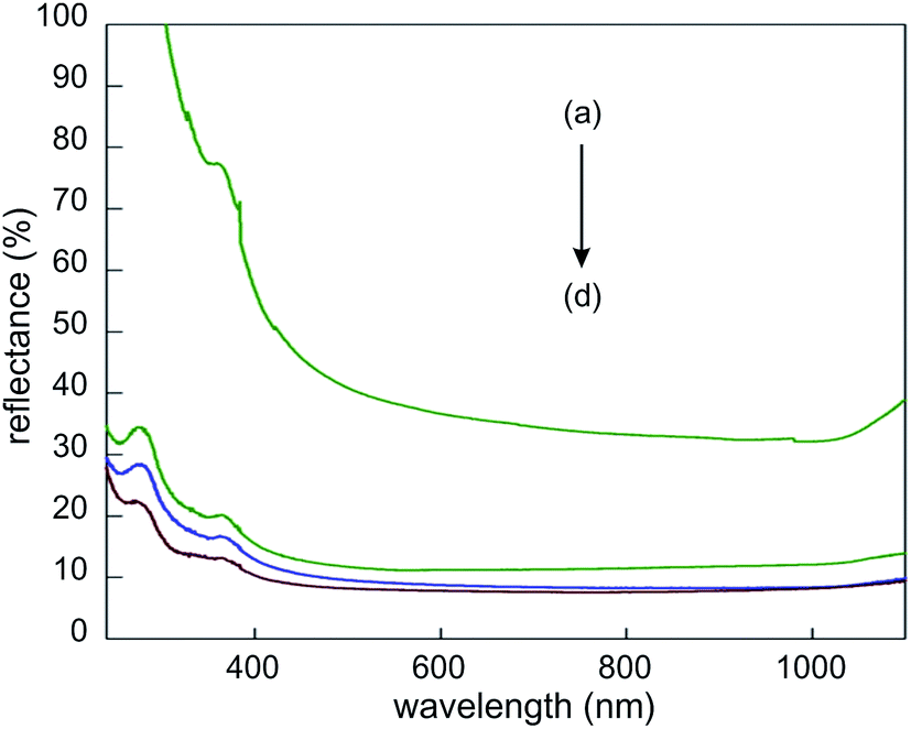 | ||
| Fig. 26 Reflectance spectra of BSi samples: (a) polished silicon; electro-deoxidized porous silicon with different deoxidation times of (b) 1 h, (c) 17 min and (d) 3 min.174 Adapted by permission of the Electrochemical Society. | ||
The FFC-Cambridge process is a potentially cheaper and simpler process for producing solar grade silicon at scales to meet industrial demands. This technique is highly versatile, and can be used to deposit thin silicon films onto metal sheets,168,175 and to fabricate free-standing nanowire arrays.176 When used to produce a porous BSi anti-reflection layer, this technique affords little material wastage, owing to its electrochemical reduction nature, in contrast to etching processes. This technique is, however, a high temperature process (∼850 °C), which can render silicon wafer prone to Mo and other metal contaminations171 and the high temperature may degrade solar cell performance, especially for wafers made from mc-Si, owing to the diffusion of impurities from grain boundaries into grains.177
3 Black silicon properties
BSi possesses a few unique properties not found in bulk silicon,40 making it an ideal candidate material for solar cell components:• Light trapping and anti-reflection, which can be exploited to allow anti-reflection coating (ARC) layers to be fabricated.178–180
• Modified band gaps controlled by impurity doping, which can be employed to design multi-junction solar cells.
• Low mechanical strength, which can be used to easily separate ultra-thin wafers from silicon ingots.
• Gettering effects, the results of large and active surfaces, which can be utilized to reduce impurities in the wafer.
3.1. Anti-reflection coating
 | ||
| Fig. 27 SEM images of (a) a KOH etching textured (100) c-Si wafer;182 and (b) anisotropic etching of a mc-Si wafer resulting in grain-dependent texturization.152 Adapted by permission of Elsevier and SPIE. | ||
Alkaline etching is anisotropic and creates undesirable steps along the grain boundaries in mc-Si wafers (Fig. 27b). Consequently, for mc-Si wafer solar cells, the most common type of solar cells available in the market, isotropic acidic texturing is often employed, affording a weighted reflectance of ∼21–25% (from 300 to 900 nm) on wafers without AR coating.80,183–185 On mc-Si wafers, dielectric layers are also used to improve the passivation and anti-reflection properties; this results in a weighted reflectance down to ∼5% for isotextures.
It is a common manufacturing trend to produce ever thinner solar wafers, for reducing material cost and relaxing the requirements on wafer impurity levels and associated carrier diffusion lengths.186,187 As wafer thickness decreases, it becomes increasingly difficult to undertake conventional wet etching, owing to its deep etching profile and relatively large wastage of silicon material. Conventional etching techniques, in general, are not appropriate on very thin wafers (<10 μm);137 yet, ARC and particularly light trapping is critical for the photon management of these thin wafers.114,188
An alternative AR solution is to use BSi. BSi helps to reduce reflectance in different ways, depending on the size and shape of its surface texture. First, there is a reflection reduction because of a multitude of interactions of light with the textured surface. Second, when the size of the texture features is large compared to the wavelength of the solar spectrum, surface scattering is responsible for an elongated light path and enhanced absorption.114,189 Third, for sub-100 nm nanostructured silicon, the surface feature sizes are so small that the surface essentially acts as an effective index medium and is optically flat.190 In this case, a smooth refractive index transition from air to bulk silicon, via the nanostructured surface, results in an effectively graded-index AR coating which affords a strongly reduced reflectance (Fig. 28).
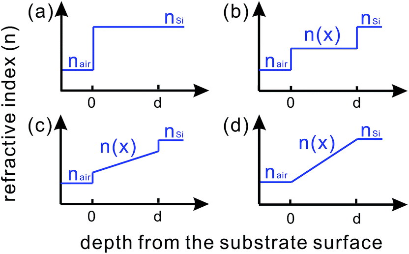 | ||
| Fig. 28 Refractive index profiles from air to (a) a silicon wafer without any ARC; (b) a silicon wafer with a porous silicon layer of constant porosity; (c) and (d) silicon wafers with gradient porosities.62 | ||
In the effective index medium region, the substrate material is mixed with air on a sub-wavelength scale. A constant porosity in BSi leads to a step change in refractive index from air to BSi, and then to bulk silicon (Fig. 28b). This porous layer is equivalent to a lower refractive index material. By creating a porosity gradient, a smoother transition in the refractive index from air to bulk silicon [Fig. 28c and d] can be achieved. These BSi layers, such as described in Fig. 28d, lead to a maximum reduction in reflectance;191–194 the overall reflectance improves as the thickness of the BSi layer increases and as the feature size of the nanostructured silicon becomes smaller.46,195 The effective medium theory predicts that a 200–300 nm thick textured graded index layer is sufficient to almost completely suppress the reflectance across the whole solar spectrum (above the silicon bandgap).96,191 It should, however, be pointed out that the relationship between silicon porosity and the corresponding refractive index is positive but not linear.46,190
Consequently, by increasing its thickness and reducing its feature size, BSi demonstrates comparable, and even superior, low reflection as compared to conventional single layer (such as SiNx) and double layer (such as TiO2/MgF2) ARC196 with a reflectance of less than 1% over a broadband reported.46,197
The AR effect of BSi works for a wide range of wavelengths and incident angles, and is polarization-independent.34,35,198 The wide spectral window of BSi is evident by its flat reflectance spectra (with the notable exception of electrochemically etched samples with a fixed porosity, which is equivalent to a homogenous layer of low refractive index material). Furthermore, the polarization and angular dependence of BSi have been tested by Xie et al. and Huang et al., on samples fabricated via metal-assisted chemical etching198 and RIE,129 respectively. Both types of samples demonstrate a low reflectance up to a large incident angle of ∼80° (Fig. 29).
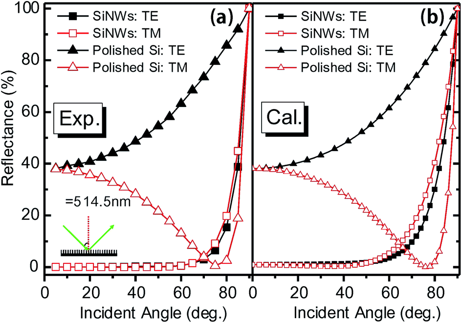 | ||
| Fig. 29 (a) Measured and (b) calculated reflectance of 800 nm long silicon nanowires for both s-polarized transverse-electric (TE) and p-polarized transverse-magnetic (TM) light at 514.5 nm, as a function of incident angle (θ). The spectra of a polished wafer is also shown for comparison.198 © IOP Publishing. Reproduced by permission of IOP Publishing. All rights reserved. | ||
| S/N | BSi fabrication method | Si type/size | V oc (mV) | J sc (mA cm−2) | FF (%) | Eff. (%) | Remarks | Ref. |
|---|---|---|---|---|---|---|---|---|
| a Unless otherwise specified, all solar cells reported here are p-type standard cells, i.e., with homojunction and passivated front surface. b Abbreviations used: open circuit voltage, Voc; short circuit current density, Jsc; fill factor, FF; efficiency, eff.; CZ, Czochralski wafers; FZ, flow zone wafers; NREL, National Renewable Energy Laboratory. c For micro-nano dual-scale surface texture, micro-pyramid surface texture is firstly developed by anisotropic alkaline etching on (100) wafers; nano-scaled structures are then coated on micro-scaled textures, via various BSi fabrication techniques, such as electrochemical etching,41 metal-assisted chemical etching,35,208,211–213 and RIE (see Section 5.2 for more details).217 d SIS solar cell: semiconductor–insulator–semiconductor solar cell (see Section 3.2.2 for more details). | ||||||||
| 1 | Electrochemical etching | c-Si (CZ), 4 cm2 | 579 | 28.8 | 76 | 12.7 | No further passivation; selective emitter | 39 |
| 2 | Electrochemical etching | c-Si (FZ), 4 cm2 | 603 | 30.4 | 78 | 14.3 | No further passivation; selective emitter | 41 |
| 3 | Electrochemical etching | c-Si (FZ), 4 cm2 | 601 | 31.3 | 78 | 14.6 | No further passivation; micro-nano dual-scale surface texture;c selective emitter | 41 |
| 4 | Stain etching | mc-Si, size not specified | 569 | 25.5 | 68 | 9.6 | No further passivation; selective emitter | 205 |
| 5 | Stain etching | mc-Si, 25 cm2 | 609 | 29.1 | 79.7 | 14.1 | No further passivation; selective emitter | 41 |
| 6 | Vapour chemical etching | Polycrystalline-Si, 25 cm2 | 540 | 24.8 | 65.6 | 9.2 | No further passivation; selective emitter | 85 |
| 7 | Vapour chemical etching | mc-Si, 25 cm2 | 550 | 22.4 | 78 | 10.0 | No further passivation; selective emitter | 89 |
| 8 | Vapour chemical etching | mc-Si, 3.2 cm2 | 560 | 31.5 | 74 | 11.8 | No further passivation; buried front contact | 206 |
| 9 | Metal-assisted chemical etching | c-Si (CZ), ∼5.76 cm2 | 578 | 28.9 | 71 | 11.7 | No further passivation | 105 |
| 10 | Metal-assisted chemical etching | mc-Si, 243.36 cm2 | 604 | 33.9 | 77.3 | 15.8 | SiO2/SiNx stacked layer passivation | 207 |
| 11 | Metal-assisted chemical etching | c-Si, 243.36 cm2 | 616 | 33.0 | 77.3 | 16.1 | SiO2 passivation; micro-nano dual-scale surface texture | 208 |
| 12 | Metal-assisted chemical etching | mc-Si, 232.26 cm2 | 624 | 36.1 | 76.2 | 16.4 | SiO2/SiNx stacked layer passivation | 209 |
| 13 | Metal-assisted chemical etching | c-Si (FZ), ∼1 cm2 | 607 | 34.9 | 77.2 | 16.4 | SiO2 passivation | 210 |
| 14 | Metal-assisted chemical etching | c-Si/243.36 cm2 | 615 | 34.6 | 76.0 | 16.5 | SiNx passivation; micro-nano dual-scale surface texture | 208 |
| 15 | Metal-assisted chemical etching | c-Si (FZ), 4 cm2 | 621 | 33.1 | 80.2 | 16.5 | Al2O3/SiNx stacked layer passivation; micro-nano dual-scale surface texture | 211 |
| 16 | Metal-assisted chemical etching | c-Si (FZ), 1 cm2 | 612 | 34.1 | 80.6 | 16.8 | SiO2 passivation; NREL tested | 34 |
| 17 | Metal-assisted chemical etching | mc-Si, 243.36 cm2 | 624 | 35.2 | 77.2 | 16.9 | SiNx passivation; selective emitter | 33 |
| 18 | Metal-assisted chemical etching | c-Si (FZ), size not specified | 615 | 35.6 | 78.2 | 17.1 | SiO2 passivation; micro-nano dual-scale surface texture; NREL tested | 35 |
| 19 | Metal-assisted chemical etching | c-Si, 243.36 cm2 | 623 | 34.6 | 77.8 | 17.1 | SiO2/SiNx stacked layer passivation; micro-nano dual-scale surface texture | 208 |
| 20 | Metal-assisted chemical etching | c-Si (CZ), 156.25 cm2 | 623 | 35.5 | 79.3 | 17.5 | SiNx passivation; micro-nano dual-scale surface texture | 212 |
| 21 | Metal-assisted chemical etching | c-Si (CZ), 0.92 cm2 | 598 | 41.3 | 75.1 | 18.2 | Al2O3 passivation | 202 |
| 22 | Metal-assisted chemical etching | c-Si (FZ), 0.8081 cm2 | 628 | 36.5 | 79.6 | 18.2 | SiO2 passivation; NREL certified | 32 |
| 23 | Metal-assisted chemical etching | c-Si, 243.36 cm2 | 639 | 37.2 | 79.1 | 18.8 | SiNx passivation; micro-nano dual-scale surface texture | 213 |
| 24 | RIE | c-Si, 0.8 cm2 | 420 | 24.1 | 65 | 6.6 | SIS solar celld | 214 |
| 25 | RIE | mc-Si, 100 cm2 | 566 | 25.0 | 72 | 10.2 | SiO2 passivation | 116 |
| 26 | RIE | c-Si, 98 cm2 | 564 | 28.6 | 73 | 11.7 | SiO2 passivation | 116 |
| 27 | RIE | c-Si (CZ), 156.25 cm2 | 611 | 32.5 | 77 | 15.1 | SiNx passivation | 115 |
| 28 | RIE | mc-Si, 243.36 cm2 | 619 | 33.5 | 77.7 | 16.1 | SiNx passivation | 215 |
| 29 | RIE | mc-Si, 243.36 cm2 | 614 | 33.8 | 78.6 | 16.3 | No passivation details specified | 126 |
| 30 | RIE | c-Si (CZ), 156.25 cm2 | 617 | 36.8 | 76 | 16.7 | SiNx passivation | 124 |
| 31 | RIE | mc-Si, 243.36 cm2 | 613 | 36.1 | 76.0 | 16.8 | SiNx passivation | 216 |
| 32 | RIE | mc-Si, 225 cm2 | 621 | 36.2 | 76.2 | 17.1 | SiNx passivation for both front and rear sides | 123 |
| 33 | RIE | c-Si, 156.25 cm2 | 623 | 35.4 | 78.2 | 17.2 | SiNx passivation; micro-nano dual-scale surface texture | 217 |
| 34 | RIE | mc-Si, 243.36 cm2 | 632 | 35.7 | 77.9 | 17.6 | SiNx passivation; selective emitter | 218 |
| 35 | RIE | c-Si (FZ), 4 cm2 | 632 | 39.2 | 75.8 | 18.7 | n-Type solar cell; Al2O3 passivation for front side and PassDop219 passivation for the rear side | 220 |
| 36 | PIII etching | mc-Si, 243.36 cm2 | 600 | 33.2 | 77.9 | 15.5 | SiNx passivation; doping performed after BSi formation | 185 |
| 37 | PIII etching | c-Si, 156.25 cm2 | 619 | 32.0 | 78.3 | 15.7 | SiNx passivation | 119 |
| 38 | PIII etching | mc-Si, 243.36 cm2 | 607 | 34.5 | 78.1 | 16.3 | SiNx passivation; doping performed before BSi formation | 204 |
| 39 | PIII etching | mc-Si, 243.36 cm2 | 613 | 34.2 | 77.6 | 16.3 | SiNx passivation | 221 |
| 40 | PIII etching | mc-Si, 243.36 cm2 | 623 | 36.0 | 77.8 | 17.5 | SiNx passivation | 222 |
| 41 | Laser texturization | c-Si (FZ), 1 cm2 | 507 | 39.2 | 72 | 14.1 | SiO2/SiNx stacked layer passivation | 200 |
| 42 | Laser texturization | c-Si (FZ), 1 cm2 | 507 | 39.2 | 71.4 | 14.2 | SiO2/SiNx stacked layer passivation | 199 |
| 43 | Laser texturization | c-Si (FZ), 7.3 cm2 | 658 | 37.3 | 75.0 | 18.4 | SiO2 passivation for both front and rear sides; double-sided buried contact solar cells | 223 |
Although BSi offers excellent optical performance, its electrical performance in solar cells is, on the whole, quite poor. In some studies, high power conversion efficiencies with BSi have been reported, in comparison to those of planar reference cells.105,205 These comparisons, however, are typically biased by poor reference cell choices, considering that the surfaces of standard solar cells are always textured. Despite their lower optical reflectance, BSi solar cells generally show lower power conversion efficiencies.207,224,225 At present, the highest reported efficiencies are 18.2% (ref. 32) (certified by National Renewable Energy Laboratory, USA) and 18.7% (ref. 220) for p-type and n-type c-Si wafer cells, respectively (Fig. 30), i.e., lower than the standard control cells (with random pyramidal textured surfaces, single-layer antireflection coatings and otherwise similar cell structures as compared to the BSi solar cells) fabricated under similar conditions (Table 2).
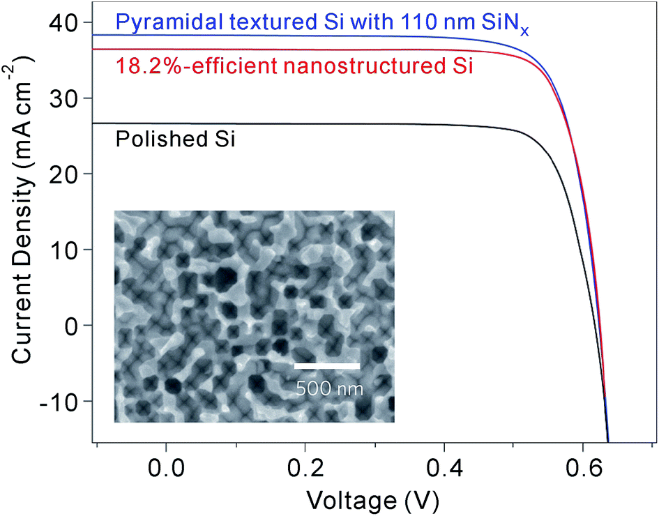 | ||
| Fig. 30 J–V curves of 18.2%-efficient nanostructured BSi, polished silicon and pyramid-textured silicon with a SiNx antireflection coating under AM1.5 illumination. Inset: top-view SEM image of the BSi solar cell.32 Reproduced by permission of Nature Publishing Group. | ||
| V oc (mV) | J sc (mA cm−2) | FF (%) | Efficiency (%) | Remarks | |
|---|---|---|---|---|---|
| Oh's p-type solar cells 32 | |||||
| Polished silicon | 617 | 26.62 | 79.6 | 13.1 | Size = 1 cm2 |
| Pyramid textured silicon with 110 nm SiNx coating | 624 | 38.26 | 78.1 | 18.6 | Size = 1 cm2 |
| BSi | 628 | 36.45 | 79.6 | 18.2 | Size = 0.8081 cm2; NREL certified |
| Repo's n-type solar cells 220 | |||||
| BSi #1 | 628 | 39.3 | 75.8 | 18.7 | Size = 4 cm2; diffusion at 890 °C |
| BSi #2 | 632 | 39.2 | 75.8 | 18.7 | Size = 4 cm2; diffusion at 910 °C |
| BSi #3 | 630 | 38.4 | 76.1 | 18.4 | Size = 4 cm2; diffusion at 930 °C |
| Pyramid textured silicon with Al2O3/SiNx stacked coating | 631 | 39.9 | 75.3 | 18.9 | Size = 4 cm2; diffusion at 910 °C |
The relatively poor performance of BSi-based solar cells is related to its nanostructured surface. Lin et al. performed light beam induced current (LBIC) analysis on a BSi solar cell with a porous surface and a reference planar solar cell.226 A short wavelength laser (e.g. 407 nm) was used to characterize the top layer of the solar cells, while a long wavelength laser (e.g. 1013 nm) was used to penetrate deeper into the surface and study the bulk silicon properties. This study shows that the bulk of BSi and planar silicon exhibit comparable performances. However, the top surface of the BSi shows a significantly lower LBIC signal compared to the reference solar cell, indicating a poorer performance of the BSi solar cell near the top surface. Yuan et al. further showed that the nanostructured layer can be effectively modeled as a dead layer, which is thinner than the actual nanostructured layer thickness.34,35
The poor solar cell performance near the nanostructured surface can be attributed to the following causes: (1) the enlarged surface area resulting in increased surface recombination; (2) the surface issuing a heavier and non-uniform doping, leading to substantial Auger recombination and/or shunts; (3) a poor contact to metal fingers. All three factors relate directly to the BSi surface texture.
It is relatively easy to understand the increased surface recombination in BSi, owing to the considerable size of its surface area and associated surface structural defects. This surface recombination may become significant, considering that conventional passivation techniques, such as chemical vapor deposition (CVD) of SiNx, still face considerable challenges in fabricating conformal dielectric coatings on rough surfaces.
A relatively subtle, but equally critical problem in BSi is related to its doping profile. Due to its large surface area, the diffusion of dopants within BSi is much more efficient than in a planar wafer. Currently, most BSi solar cells are still fabricated based on the procedure used for conventionally textured solar cells. Consequently, this leads to very high doping concentrations in BSi emitters, and causes considerable Auger recombination. Such high doping concentrations may even render the effective carrier lifetime independent of the surface area.32 Oh et al. showed that in high doping regions, Auger recombination is a dominating factor for carrier losses in BSi solar cells, while the surface recombination dominates only in low doping regions; in the medium doping region (sheet resistance of ∼90 to 210 Ω ☐−1), both surface and Auger recombination mechanisms are important.32
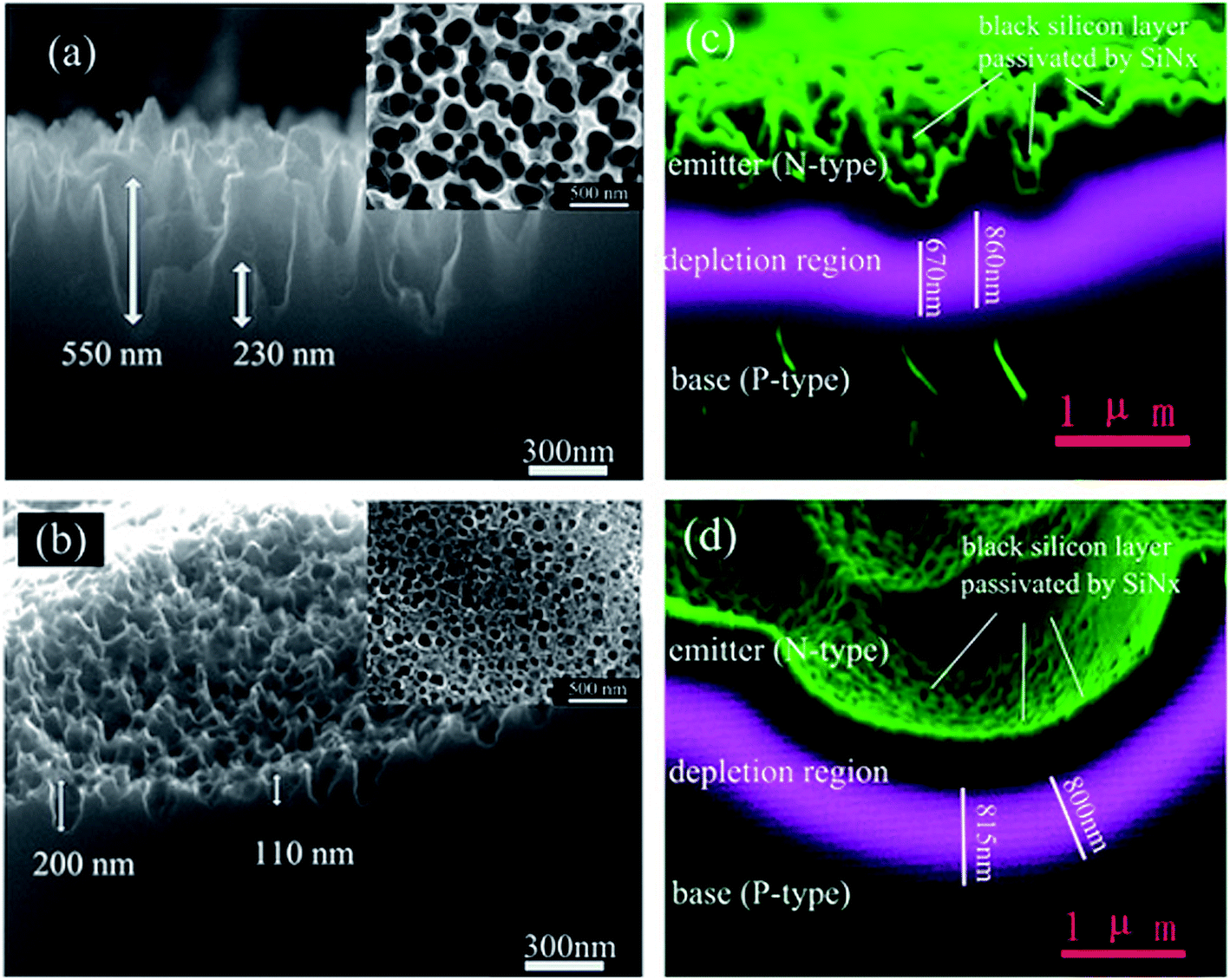
In addition to a high doping concentration, non-uniformity in the dopant distribution may also present an issue, especially in nanostructures with high-aspect ratios. For example, Shen et al. compared the doping profiles of two fabrication methods.204 In the first process, the BSi texture was finished first, followed by high temperature doping (Fig. 31a); in the second, the sequence of doping and BSi formation using PIII etching was reversed (Fig. 31b). It was shown that with a thick BSi layer, coated on a silicon substrate by the first process, more dopants entered the nanostructured “needles” via the side walls, while fewer dopants entered the bulk silicon owing to the smaller contact area. Such non-uniform doping resulted in a varied thickness of the depletion region, a corresponding lateral field and a lower shunt resistance, as deduced from electron beam-induced current (EBIC) imaging (Fig. 31c). In contrast, with doping performed before the BSi formation, the second process afforded a shallower BSi layer and a more uniform doping profile, contributing to a higher power conversion efficiency of 16.3%, in comparison to 15.5% achieved using the first process.204
 | ||
| Fig. 31 BSi fabricated with PIII etching performed (a) before doping and (b) after doping; (c) and (d) are cross-section views of EBIC images corresponding to (a) and (b), respectively.204 Reproduced by permission of Elsevier. | ||
The same problem of low shunt resistance and high leakage current due to non-uniform doping in BSi was also found by Hsu et al.209 Hsu and co-workers fabricated BSi with different nano-rod lengths using Ag-assisted chemical etching on 6′′ wafers, and produced solar cells using standard fabrication procedures. Electroluminescence (EL) imaging characterization showed that BSi with long nano-rods led to more widespread non-uniform doping, largely suppressing the luminescence in silicon solar cells and exhibiting more dark areas (Fig. 32). In contrast, the shorter, 100 nm nano-rod coated wafers contained far fewer defect areas, indicating a more uniform doping profile (Fig. 32c).
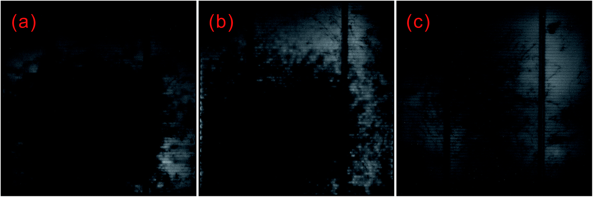 | ||
| Fig. 32 EL images of BSi solar cells covered by different thickness of nano-rods: (a) 1 μm; (b) 600 nm; and (c) 100 nm.209 The black regions contain more defects, and correspond to non-uniform doped areas. | ||
It is also problematic to form good metal contacts on nanostructured surfaces. In BSi that contains deep pores, metal cannot completely bridge the gaps between nanostructures, resulting in poor contact (Fig. 33).220 Moreover, some needle-like nanostructures have “self-cleaning” or super-hydrophobic properties, posing significant difficulties for screen printed metal contacts.25,119
 | ||
| Fig. 33 SEM image of a BSi sample covered by printed front metal contact.220 Reproduced by permission of Elsevier. | ||
When a passivation layer, such as SiNx, is deposited onto BSi, the non-uniform thickness of SiNx coating on a roughed silicon surface makes the contact formation even more challenging. For example, in nanostructured valleys with a thick SiNx coating, the silver paste cannot etch through the dielectric layer, thus raising contact resistance.221,225
Due to these factors, the overall power conversion efficiency of BSi solar cells is typically low, and the optical gain from BSi often cannot compensate for its electrical losses. In particular, owing to the enlarged surface area and surface defects, heavy doping, and the associated surface and Auger recombination in BSi emitters, the external quantum efficiency (EQE) of BSi solar cells is especially poor in the short wavelength region.119,227 Note that short wavelength (or high energy) photons are strongly absorbed in the top layer of a silicon wafer where the BSi resides. This is a typical characteristic of BSi solar cells.
Thickness control. The conflicting optical and electrical demands of BSi require a tradeoff in the optimized morphologies for solar cell applications. A thicker nanostructured layer is required to minimize the surface reflectance, while such a surface structure results in a significantly large surface area for recombination and poses considerable challenges for doping and metal contact formation. In order to attain an improved solar cell performance, the thickness of the nanostructured layer must be tightly controlled.
To this end, several optimal thickness values have been suggested, according to the surface morphologies of the BSi and fabrication technique used. For porous silicon made via electrochemical HF etching and stain etching, it has been proposed that a ∼100 nm thick BSi is required to balance the optical gain against electrical losses.40,41 In contrast, Lee et al. suggested that the optimal depth of RIE nano-structures to achieve the same aim was about 200–400 nm.126 Using a similar technique, i.e., PIII etching, Zhong et al. fabricated a series of solar cells, with different nano-hillock thicknesses from 150 to 600 nm. They showed that the optimal height of their nanostructures was 300 nm.225 Yuan et al. textured their silicon wafers using metal-assisted chemical etching, and found that a thickness around 500 nm yielded the highest solar cell efficiency.34 In a later study using Ag-assisted chemical etching, Oh et al. reported a very high BSi PV efficiency of 18.2%, resulting from BSi nanostructure thicknesses of less than 400 nm.32 For laser irradiation induced BSi, the surface is micro-structured, and the corresponding texture layer thickness is much larger, of the order of several μm.199
Overall, the optimal thickness for nanostructured BSi layer is several hundreds of nm; this value may be increased for a lower reflectance, provided that the electrical issues are properly addressed, i.e., by applying improved surface passivation and doping strategies.
Surface cleaning. BSi formation not only increases the surface area, but also creates a considerable number of defects within the micro- or nanostructured surface; a thorough cleaning or post-etching process is essential to remove these defects. For example, RIE leads to the formation of a ∼50 nm thick defect layer, which seriously degrades minority carrier lifetime in a solar cell.227 Kumaravelu and co-workers compared the effective carrier lifetime (τ) of a RIE textured wafer against a planar control wafer using quasi-steady-state photo conductance.78 In comparison to a large τ of ∼400 μs in the control wafer, the lifetime of the RIE-treated BSi decreases to merely 2–3 μs. After defect removal by etching in HNO3–HF (50
:1), its lifetime rises again to ∼36 μs. The still lower lifetime compared to that of the control wafer was attributed to the increased surface area.78 Similarly, several other research groups also noticed that a thorough defect removal etching was critical for improving the carrier lifetime in RIE-treated BSi79,228 and increasing photovoltaic efficiency in PIII-treated BSi.222
For metal-assisted chemical etching, a deep and thorough etching becomes even more critical.227 First, this etching creates a sub-oxidized surface with a significant number of surface defects. Second, the surface of the chemically etched nanostructures is very rough; on top of the relatively big nanostructures (∼100 nm), there are also many small protrusions with a size of ∼2–5 nm. These small protrusions have little impact on the optical reflectance of BSi, but cause a substantial increase in its surface area. Third, it is likely that a small trace of metal ions diffuse into silicon during the BSi fabrication; this issue becomes even more vital if a high temperature process (e.g. doping) follows the BSi formation.
To address these problems, Algasinger and co-workers performed a modified RCA cleaning, successfully removing the surface defects and gold nanoparticles used for the metal-assisted chemical etching.227 This cleaning procedure also etched away the small nano-protrusions, which was apparent by the absence of silicon photoluminescence after the cleaning process. The reduced surface area makes the surface passivation much easier to implement. Consequently, upon depositing an Al2O3 layer onto the BSi surface, using atomic layer deposition (ALD; see Section 4.4), a high carrier lifetime of ∼500 μs was measured, which is one order of magnitude higher than that in untreated BSi.227 Similarly, for laser treated micro-structured surfaces, Nayak et al. showed that surface cleaning, using NaOH solution rinse followed by an isotropic etching (HNO3–CH3COOH–HF, 30:10:4), played an important role in the removal of redeposited materials and induced defects, and improved solar cell efficiencies.199
Doping profile control. The large surface area of BSi means the mass transfer rate of dopants is faster than that of planar silicon. Zhong et al. compared that the resistance of a BSi wafer and a planar wafer with the same doping conditions and found that the BSi had a lower resistance, indicating a higher level of doping.185 In order to control the BSi doping concentration and minimize Auger recombination, Zhong and co-workers showed that a lower doping temperature should be employed. They performed doping at different temperatures (815, 820, 825, 830 and 835 °C) in PIII-treated BSi samples, and found that doping at 815 °C led to the highest EQE in the short wavelength region (<550 nm).185 Repo et al. arrived at the same conclusion by performing doping in RIE-treated BSi samples at 890, 910, and 930 °C, and discovered that their internal quantum efficiency (IQE) reduced with increasing doping temperature.220
Oh et al. adopted a different strategy to remove the highly doped regions in BSi. They performed doping at 850 °C with a subsequent anisotropic tetramethyl-ammonium-hydroxide (TMAH) etch procedure. This etching had two effects: first, the highly doped dead layer on the surface of the BSi was removed; second, the total surface area was reduced, owing to a reduction in the nanostructured layer thickness and an enlargement of its surface feature size, but at the expense of increased reflectance (Fig. 34).32 Based on this method, an excellent BSi solar cell performance with 18.2% efficiency was realized.
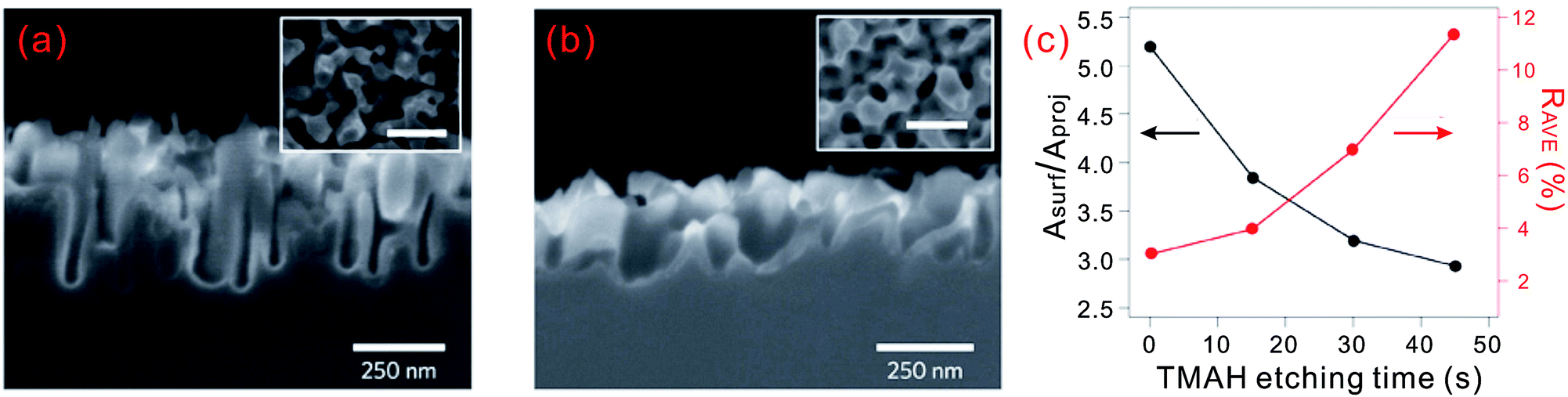 | ||
| Fig. 34 SEM images of the morphologies of nanostructured silicon surface, fabricated with Ag-assisted chemical etching (a) before and (b) after 30 s of TMAH back-etching. (a) and (b) show the side views of the BSi samples, while the insets represent their top views. The white conformal layer in each side view of the samples show a thermal oxide passivation layer. (c) Ratios of the actual surface area over the projected planar surface area (Asurf/Aproj) and the reflectance of the TMAH back-etched BSi, as a function of back-etching time.32 Reproduced by permission of Nature Publishing Group. | ||
Another method to circumvent the doping problem associated with BSi is to dope the wafer prior to texturization. This approach has been successfully adopted by some groups.33,204 Nevertheless, a high doping concentration at the emitter is likely to change the surface morphology of the resulting BSi. For example, during metal-assisted chemical etching, the surface feature size tends to increase in line with the doping level of the silicon substrate, and the impact of doping on the etching rate is not yet fully understood.92 Further work is thus required before a wider deployment of this doping strategy can be adopted.
Other issues. Owing to the importance of passivation, especially for BSi solar cells, we devote Section 4 of this paper to this topic.
For nanostructures with a surface feature size below the wavelength of visible light, the surface acts as an effective index medium and can be considered to be optically flat. Hence, the normal incident light will penetrate through the wafer without undergoing scattering. In order to increase the optical path length in silicon and to enhance the absorption of long wavelength light, it is important to roughen its back surface for light trapping (Section 5.2).34 Furthermore, due to the higher surface resistance in BSi compared to that of a planar wafer, it is necessary to reoptimize the metal-grid within BSi solar cells to enhance the charge collection efficiency.205
Strategy summary. To summarize, current fabrication methods of BSi solar cells are still largely based on conventional solar cell technologies, but a number of modifications are required to improve their cell efficiencies. More specifically, nanostructures of low aspect ratio should be employed to balance the optical gain and electrical losses; thorough removal of surface defects is critical to maximize carrier lifetime; a modified doping strategy should be developed to minimize Auger recombination in the surface layer. Good passivation is important in BSi, due to its enlarged surface area, and the solar cell architecture requires re-optimization, by methods such as incorporating light trapping structures and applying a finer and denser metal grid for a higher charge collection efficiency. By undertaking these improvements, it is likely that the efficiency of BSi solar cells will advance even further in the near future, with a >20% efficient solar cell concept recently envisioned.32
It is encouraging to note that the first trial-run of BSi solar cells in a production line at Natcore Technology has recently been performed, yielding an efficiency of 15.7%; this compares with an efficiency of 17–19% for conventional reference cells.229,230 JA Solar, one of the major solar cell manufacturers, has reported an efficiency of 18.3% in their mc-BSi solar cells and introduced a BSi solar cell module rated at 270 W.231 While the efficiency of BSi solar cells is likely to be further improved via process optimization, these results demonstrate that BSi solar cells can be integrated with existing industrial production lines.
Natcore Technology has claimed that solar cell processing cost savings of up to 23.5% per cell could be made with BSi.229,230 However, this number is likely to be over-optimistic. In a different report, it was estimated that the savings in solar cell processing costs and the overall manufacturing costs could be up to 8% and 3%, respectively, via the incorporation of BSi technology.232
However, BSi also faces a few technical challenges in both its optical characteristics (Section 3.1.1) and electrical performance (Section 3.1.2). In particular, the optical trapping effect in nanostructured BSi could be very poor, unlike that of microstructured pyramidal structures, which is commonly used in c-Si solar cells. On one hand, the market entry barrier for BSi technology is lower in mc-Si and thin c-Si solar cells, where it is difficult or impossible to perform conventional alkaline etching. On the other hand, light trapping becomes even more critical, particularly for thin c-Si solar cells. Nevertheless, implementing light trapping on thin substrates without wafer breakage is likely to be a challenging task.233 One alternative option is to increase the feature size of BSi, in order to retain the light trapping function at a slight degradation of surface reflection. Based on the optical modeling of periodic pyramidal-like structures, Sai and co-workers have suggested that a sub-microstructured surface (with period >∼500 nm) could retain both low surface reflection and good light trapping effects.234
3.2. Novel solar cell architectures
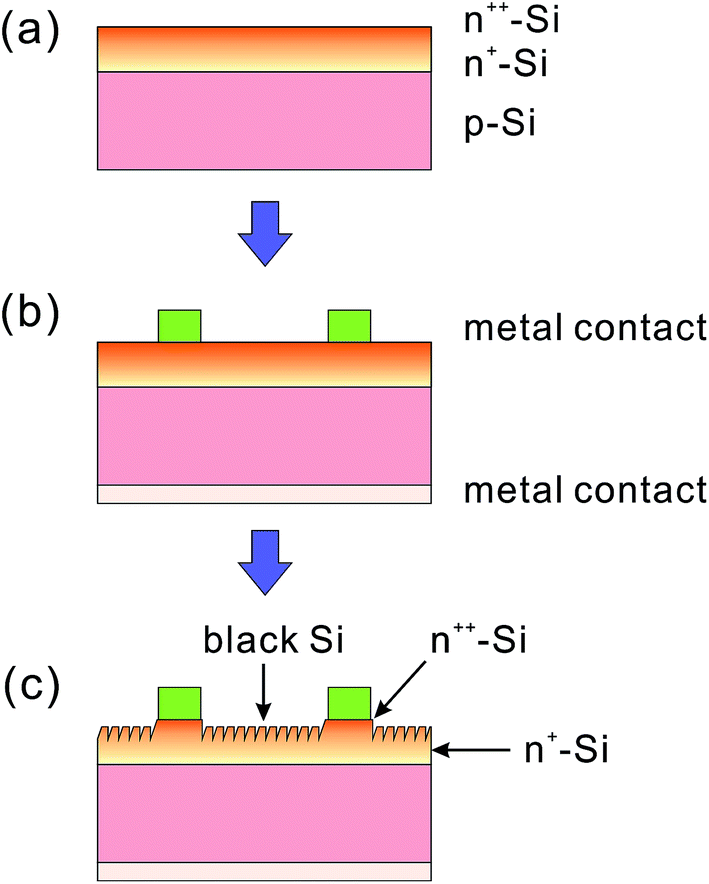 | ||
| Fig. 35 Typical fabrication procedures to create a selective emitter BSi solar cell: (a) heavy doping; (b) metallization; and (c) back-etching.41 | ||
In this design, the BSi fabrication leads to the simultaneous formation of a selective emitter, via a back-etching process to remove the top heavily-doped dead layer. Existing etching methods have been employed previously in the fabrication of this type of solar cell.33,40,41,85,205 Since pre-deposited metal fingers may be damaged during the etch process, strategies are used to minimize such effects. One method is to perform a quick etching with a large current density but for a short duration, i.e., 3–4 s using electrochemical etching,40,41 or performing a rapid stain etching.205 Another method is to apply a polymeric protection film onto the metal grid during the etching, which can be removed afterwards using acetone.
However, this coating may cover ∼0.1 mm of silicon next to the metal fingers, and prevent the formation of BSi in those areas.41 Based on these methods, 25 cm2 mc-Si selective emitter solar cells coated with porous silicon have been fabricated with ∼14% efficiencies, without applying texturization, passivation, or additional ARC.41 One additional method to minimize metal contact damage is to employ a gentler etch, such as chemical vapour etching. Rabha et al. used this to fabricate a selective emitter solar cell. The power conversion efficiency went from 7.7 to 9.2% after the back-etching process, without any passivation or additional ARC, in 25 cm2 mc-Si solar cells.85 In contrast, Wang et al. applied SiNx passivation on their selective emitter solar cells, formed via Ag catalyzed back etching. Here, wax was used to protect the metal contact formation area on the silicon substrate; and the metal fingers were printed after SiNx deposition. Efficiencies up to 16.94% were reported using this methodology.33
It is also worth mentioning the experiment of Moon and co-workers, which used porous silicon as a sacrificial layer to create a high-low doping profile for selective emitter solar cells (Fig. 36).235 They used stain etching to fabricate porous silicon, part of which was selectively removed. The remaining porous silicon acted as a mask to lower the doping concentration in underlying silicon. This mask can be etched away after the doping process. Consequently, a silicon wafer with alternating doping concentrations is fabricated. The resistances in the high- and low-doped regions were measured at 30–35 and 97–474 Ω ☐−1, respectively. A low cost doping source, H3PO4–methanol, has been used in this case, instead of POCl3 which is used commercially. As yet, no solar cells have been fabricated using this type of wafer.
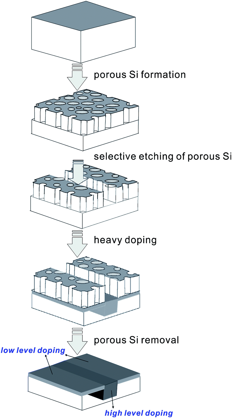 | ||
| Fig. 36 Fabrication procedures to produce a high-low doping profile using BSi as a sacrificing layer.235 Adapted by permission of Elsevier. | ||
 | ||
| Fig. 37 A schematic of a semiconductor–insulator–semiconductor solar cell. | ||
Füchsel et al. fabricated a SIS solar cell using RIE-treated BSi.214 They sputtered indium-doped tin oxide (ITO) onto the BSi to form the front contact. However, the conformality of the ITO film is very poor, especially on high aspect ratio BSi (Fig. 38). The sputtered ITO quickly seals the silicon nano-pores without completely filling them, and merges into a film. Consequently, despite the fact that it has higher Isc because of a reduced reflectance, the SIS solar cell offers lower Voc, lower fill factor and overall lower power conversion efficiency (6.6% for low aspect ratio BSi) as compared to a SIS solar cell on a planar silicon substrate (6.9%); this is caused by the poor ITO coverage over BSi as well as the enlarged ITO/BSi interface. The power conversion efficiency of high aspect ratio BSi is even poorer.214 In addition, the reflectance of the BSi increases from ∼1–3% to ∼7% after ITO coating, because of the refractive index mismatch between ITO and the BSi.
 | ||
| Fig. 38 700 nm Sputtered ITO film-coated BSi with different aspect ratios: (a) BSi composed of nano-rods with diameters ≈ 100 nm and lengths ≈ 500 nm; (b) BSi covered by nano-needles with diameters ≈ 50 nm and lengths ≈ 1.7 μm.214 Adapted by permission of SPIE. | ||
Instead of sputtering, Otto and co-workers deposited a thin layer (up to 88 nm) of ZnO and Al doped ZnO (ZnO–Al) onto BSi using atomic layer deposition (ALD; see Section 4.4).238 Excellent TCO conformal coating was achieved for nano-spikes of up to 1 μm high (Fig. 39). At low deposition temperatures (∼100 °C), the grain size in the film was small, and the resistivity relatively high [(1.01 ± 0.22) × 104 Ω ☐−1 at 120 °C]. At 220 °C, the grain size was enlarged, and surface resistivity dropped to 60.3 ± 1.3 Ω ☐−1. Upon further increasing the deposition temperature, however, defect formation resulted in an increased resistivity. This temperature dependence was also observed by Steglich et al.239 The thin TCO coating also had little impact on the reflectance of BSi, resulting in a flat and low reflectance below 5% in both the visible and near-IR regions.238
 | ||
| Fig. 39 SEM images of an ALD-deposited ZnO–Al layer sitting on top of (a) a shallow BSi structure and (b) a deep BSi structure, with good conformality; (c) high resolution TEM image confirming the good conformality between ZnO (top), amorphous oxide (middle), and silicon (bottom).238 Reproduced by permission of John Wiley & Sons, Inc. | ||
Otto et al. also fabricated an Al2O3 film onto a nanostructured BSi sample (with nano-needle diameters of ∼150 nm and depths of ∼1.7 μm) using ALD; this film acted as the insulating layer in a SIS cell. The Al2O3 passivated BSi exhibits an excellent lifetime of 173 μs, comparable to that of planar silicon (446 μs) at an injection level of 1015 cm−3.240 It is expected that these highly conformal insulator and ITO coatings will further boost the efficiency of BSi SIS cells, with an absolute efficiency gain of 1–1.5%, over those made of a planar silicon substrates.114
When silicon substrates are treated by a fs-laser process in SF6, the surface is micro-structured with hillocks several μm high. During this process, sulfur atoms diffuse into silicon, forming an intermediate band and extending the absorption spectra of BSi to 2500 nm.241 This sulfur doping effectively creates an n-Si emitter in the laser-treated area.242
Based on this property, a tandem solar cell with two emitters was fabricated by Guenther et al.:241 one is a conventional front emitter and the other is sulfur doped emitter at the rear side of the cell, while the p-substrate acts as a base for both emitters (Fig. 40). In this tandem n+–p–n+ solar cell, the front emitter is responsible for absorbing high energy photons, while the back emitter with an intermediate band absorbs long wavelength photons in the visible and IR regions. The p–n junction at the rear side is shown to generate a Voc of ∼17 mV and a Jsc of ∼1 mA cm−2.
 | ||
| Fig. 40 Tandem n+–p–n+ solar cell using laser treated BSi.241 | ||
However, the laser treatment and sulfur doping lead to many defects in the substrate. To retain a sufficient sulfur concentration, one is also restricted to low temperature annealing, which removes structural defects but also significantly decreases sulfur concentration and reduces photon absorption in the IR region. Consequently, this tandem cell only affords a power conversion efficiency of 4.5%.241,242
Grau et al. used HF etching to form a porous silicon Bragg reflector with alternating high/low porosities.243 This reflector is inserted between a thin film silicon cell and a cheap substrate, such as glass. Depending on the porosity and thickness of the porous layer, the reflectivity of the Bragg reflector can top 90% over a broad range, i.e., 750–1100 nm. This enhanced reflection improves light absorption in thin film silicon solar cells and boosts device performance.244 However, the overall efficiency gain from this Bragg reflector will not be very significant, owing to its modest overall back-reflecting properties and high back-interface carrier recombination.243
3.3. Flexible/thin wafer production
Thin film silicon solar cells (thickness < 30 μm) are preferred due to their lower material cost, and relaxed requirements on wafer quality.245 Owing to its weak mechanical strength, porous silicon has been employed as a separation layer to produce such thin film solar cells in a kerfless porous silicon process (Fig. 41). This method offers a significant advantage over the conventional wafer-sawing technique in reducing silicon wastage.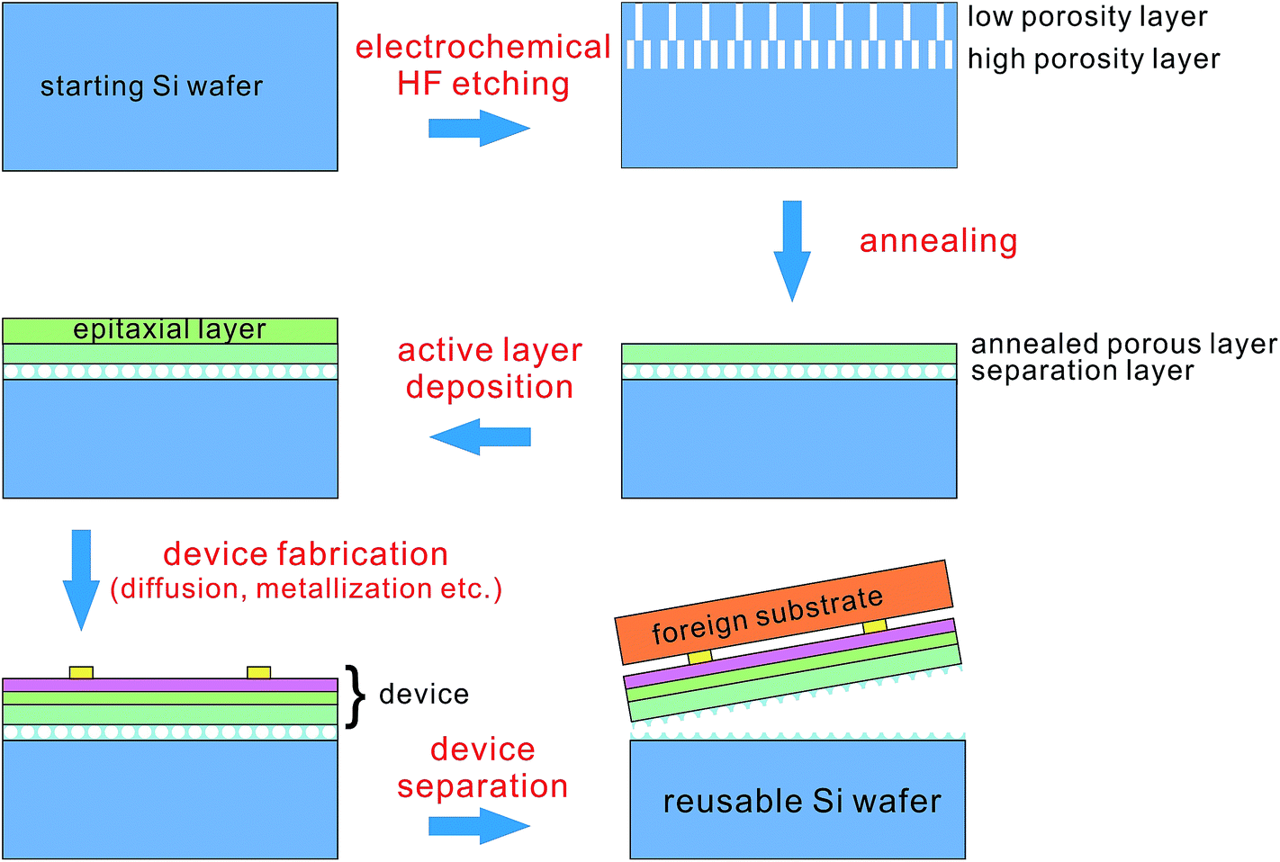 | ||
| Fig. 41 Using porous silicon as a separation layer to produce thin film silicon solar cells.245 | ||
In a typical fabrication process, porous silicon is first formed by anodization in HF and ethanol or acetic acid solution. A top layer with low porosity (10–20%) and a bottom layer of high porosity (50–70%) are fabricated by adjusting current density and/or changing [HF] during the electrochemical etching.245 Upon annealing at a high temperature (>1000 °C) in a H2 environment, the top (low porosity) layer closes its pores and becomes smooth in order to reduce surface energy; this layer subsequently serves as a platform for epitaxial deposition of silicon, typically via CVD using SiH4. The epitaxial silicon film can be used to fabricate solar cells, via diffusion, metallization and so forth. After device fabrication, the completed solar cell is glued to a cheap foreign substrate, such as glass. In the meantime, annealing of the bottom (high porosity) layer leads to the formation of voids and nano-pillars connecting the top low porosity layer to the initial silicon substrate. This high porosity layer serves as a separation layer, from which the solar cell can be separated from the initial silicon substrate by applying a mechanical force.245 Based on this concept, many similar processes for fabricating thin film c-Si solar cells have been developed, with differences being mainly in the sequence of epitaxial layer deposition, device fabrication and layer separation/transfer.245
Using the kerfless porous silicon process, Kajari-Schröder et al. produced a 30 μm thick thin and flexible silicon film (Fig. 42). The separation layer used is relatively thin (∼200 nm), and consists of nano-pillars with diameters of ∼40–100 nm at the narrowest points after annealing. These nano-pillars cover about 3% of the total substrate area, and can be broken off relatively easily.246 Radhakrishnan et al. demonstrated that the defects in the epitaxial layer created by this porous silicon-based layer transfer process can be effectively controlled, leading to high minority carrier lifetimes exceeding 100 μs.247,248 Based on this process and a back-contact back-junction cell design,249 Solexel, Inc. has reported a 20.62% efficiency for a 156 mm × 156 mm full-square ultrathin (∼35 μm thick) silicon solar cell; their roadmap indicates a 23.5% cell and a 22% module efficiency target, respectively.250,251
 | ||
| Fig. 42 SEM images of (a) a low porosity silicon layer after epitaxial deposition (top), sitting on top of a silicon substrate (bottom) via a high porosity separation layer (middle); and (b) the tilted view of the separation layer after the top layer is lifted off. (c) Photograph of the top layer (30 μm thick, 9 × 9 cm2 large).246 Adapted by permission of Elsevier. | ||
Instead of using two layers of porous silicon, Gordon and co-workers fabricated a thin silicon film, by directly annealing a single periodic silicon nano-pore array (Fig. 43a).252 Currently this pore array is fabricated via RIE through a lithographically defined mask, though a low cost nano-imprint defined mask in combination with HF anodization could potentially replace this fabrication technique. Upon annealing for 45–60 min in H2 at 1150 °C, a 3 μm thick pore array (Fig. 43b) is converted to a 1 μm thick film, separated by an extended void from the initial substrate (Fig. 43c).252 A proof-of-concept solar cell with 4.1% power conversion efficiency has been made, based on this 1 μm thick wafer.252
 | ||
| Fig. 43 (a) Fabrication procedures to produce thin silicon films in an epifree process: (1) pore formation; (2) annealing; (3) the first side of the solar cell process; (4) thin film bonding to a low cost substrate; (5) the second side of the solar cell process and reuse of the initial substrate. SEM images of side views of (b) a nano-pore array in a silicon substrate and (c) formation of an extended void and a 1 μm thick overlaying film after annealing the silicon nanopore array.252 Adapted by permission of Elsevier. | ||
It is also worth mentioning the flexible BSi produced by Mei et al.253 They used laser irradiation to micro-structure the surface of a silicon-on-insulator (SOI) wafer. Following the laser treatment, the SiO2 layer in the SOI wafer is etched away, and the isolated top layer functions as a thin and flexible BSi film, with absorption over 97% in the visible region. This flexible BSi can be potentially used for photo-detectors, thermal-electric generation, or solar thermal receivers.253,254 While used as a solar thermal receiver, this flexible BSi demonstrates good heat transfer and light absorption efficiencies, 13% higher than that of anodized aluminium.254
While developing thin silicon films is a trend in the solar industry, there remain many technical challenges for the kerfless porous silicon process, such as improving film quality and reducing wafer crack during the lift-off process.
3.4. Gettering
Porous silicon may serve as a gettering agent to remove impurities from bulk silicon during the annealing process, owing to its large surface area and high surface reactivity.255–258 The optimized annealing temperature varies from 900 to 1000 °C depending on the experimental setup and ambient environment.255–257 This porous layering can be etched away after the annealing process. Nouri et al. showed that this gettering process improved mc-Si quality, with an absolute solar cell efficiency gain of ∼1.5% in their case.257The porous silicon can also be used to reduce the impurity level in epitaxial deposited silicon layers (Fig. 42), with a gettering coefficient of ∼103 to 104 in decreasing metal contamination.259 Although the presence of this porous layer increases surface area and the associated interfacial recombination rate (∼250 times higher than that at the interface of an epitaxial layer and a flat p+-Si substrate), this problem can be mitigated via introducing an epitaxially grown back surface field on top of the porous silicon; this prevents minority carriers in the epitaxial layer from getting close to the highly recombinative porous interface.260 Consequently, it has been shown that the surface recombination rate is reduced from ∼2.5 × 105 cm s−1 to ∼1–2 × 103 cm s−1, comparable to that on bulk silicon surfaces.260
4 Passivation methods
Surface passivation is essential for high efficiency solar cells.261 For BSi, it is believed that the surface nanostructures provide good passivation as their feature sizes decrease to a few nm.39 This is because the bandgap of the nanostructured silicon is significantly higher than bulk silicon due to quantum confinement effects, and minority carriers generated in the bulk are thus prevented from getting close to the surface owing to a bandgap offset. Indeed, porous silicon produced via stain etching and electrochemical HF etching exhibits ∼20% higher lifetime (τ) than unpassivated planar silicon. However, the absolute value of τ passivated by porous silicon amounts to only ∼3.5 μs.41 This value is far less than that can be obtained by using dielectric passivation materials (i.e., SiNx, SiO2, and Al2O3) or a-Si, when ms lifetimes are achievable. Consequently, although porous silicon passivated BSi solar cells demonstrate higher efficiencies than un-passivated solar cells, their absolute values are on the lower side (∼10–14%).84,89As the feature size of nanostructures increases, i.e., to several hundreds of nm, the minority carrier mirror effect becomes very weak. In addition, the surface area of nanostructured BSi is significantly larger than that of planar silicon. Hence, good passivation becomes vital for BSi solar cells. In this section, we will examine the characters of the four most popular passivation materials used in silicon solar cells, including SiNx, a-Si, SiO2 and Al2O3; and review their application in passivating BSi. Our discussion will focus on Al2O3 fabricated via atomic layer deposition (ALD), due to its excellent conformality to nanostructured surfaces and increasing popularity in solar cell applications.
4.1. SiNx
SiNx is currently the industrial standard used to passivate the n-type emitter of p-type silicon wafer solar cells. It is deposited onto silicon using ammonia and silane mixtures through plasma-enhanced CVD (PECVD) at ∼400 °C.262 The relative weight of silicon and nitrogen can be adjusted by changing the flow rate of ammonia and silane. N2 may also be added into the gas mixture in order to lower the silicon content, improve the etching rate of SiNx (for forming the metal contact), minimize its UV light absorption, and maintain a high minority time.263 In Si-rich SiNx, the passivation is mainly governed by chemical passivation, i.e., by reducing the number of surface dangling bonds. As the nitrogen content increases, a high density of fixed positive charge (Qf = ∼1012 cm−2) develops.264,265 This positive interfacial charge is beneficial for passivating n-Si through field effect passivation. Essentially, an accumulation layer is created near the silicon surface due to the positive charge; thereby reducing the minority carrier concentration at the surface.264Owing to its good chemical passivation and positive interfacial charge, SiNx passivation works for n-Si of arbitrary doping concentrations, and lightly doped p-Si; but it is less ideal for heavily doped p-Si.266 Based on SiNx passivation, very low surface recombination rate of 6 and 15 cm s−1 have been reported for 1.5 Ω × cm n-Si and p-Si, respectively.267–269 However, under low illumination conditions, the passivation effect in lightly p-doped wafers may degrade due to additional bulk recombination in the inversion layer close to the surface.265
Since solar cell emitters are always heavily doped and SiNx does not work for p+-Si, its passivation is limited to p-type solar cells (with n+ emitters). In addition to its role of passivation, a quarter-wavelength thick SiNx film also acts as an AR layer and is commonly used in commercial solar cells. SiNx has been employed for passivating n+ BSi emitters fabricated via various processes, such as metal-assisted chemical etching,33,207 RIE,115 and PIII etching.225,270 It greatly improved BSi solar cell efficiency from 11.5 to 14.9% in Liu's experiments.207 However, since SiNx is often deposited via PECVD, its surface conformality is relatively poor for high aspect ratio BSi (Fig. 44a).
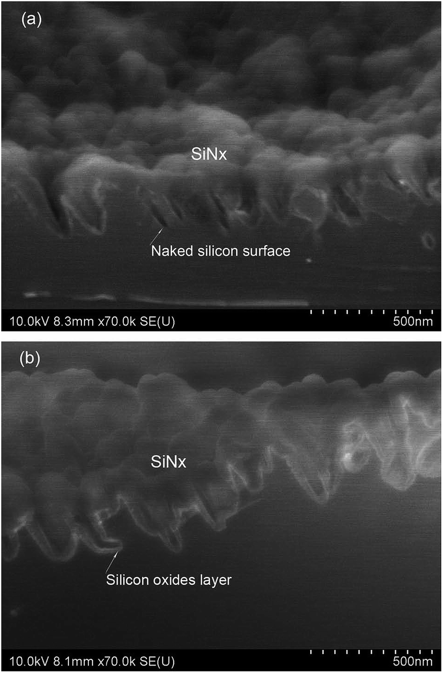 | ||
| Fig. 44 SEM images of BSi coated with (a) 80 nm SiNx; and (b) 20 nm thermal oxide and 60 nm SiNx.207 Reproduced by permission of John Wiley & Sons, Inc. | ||
It has been reported that the passivation effect of SiNx improves as its film thickness increases, but saturates when its film thickness exceeds ∼20 nm for a planar silicon wafer.271,272 Nevertheless, Liu et al. noticed that in the case of BSi, thicker SiNx film afforded better passivation. Unfortunately, a thick SiNx film also increases serial resistance for printed metal contacts. Consequently, a trade-off is required and a 77 nm thick SiNx offers a higher solar cell efficiency than those of 44 and 100 nm thick in Liu's experiments.270
4.2. Amorphous silicon (a-Si)
a-Si can be deposited via PECVD at a relatively low temperature between 200 and 250 °C.273 It forms a good interface to c-Si, thus affording strong chemical passivation, and can be used to passivate both p- and n-Si in conjunction with hydrogen annealing.273–276 Silicon surface recombination rates as low as 2 cm s−1 have been demonstrated with a-Si passivation.264 While employed in solar cells, minority carrier lifetimes greater than 5 ms and Voc up to 738 mV have been demonstrated with post-deposition plasma-hydrogenation and annealing.277 However, a-Si strongly absorbs in the visible region of the solar spectrum, and is not thermally stable.266,274–276 Owing to the use of PECVD, the conformality of a-Si on BSi is likely to be problematic. Therefore, to date, no a-Si passivation method has been reported.4.3. SiO2
Thermal oxide provides very good chemical passivation, reducing silicon interfacial defects to 109 to 1010 eV−1 cm−2.264,265,278 It also contains a small amount of positive fixed charge with a density of 1010 to 1011 cm−2, affording a weak field passivation effect.264,265 It can be used to passivate either n- or p-Si of arbitrary doping concentrations with excellent surface conformality. However, the positive interfacial charge implies that the passivation effect on a p+ emitter is likely inferior than that on an n+-emitter.Nevertheless, with the “alneal” process, Kerr and co-workers successfully passivated p+ wafers using thermal oxide.279 Here, a layer of Al was pre-deposited on an oxidized wafer before annealing. During the subsequent annealing (at 400 °C for 30 min in forming gas), the oxidization of Al with water residue in the oxide layer released atomic hydrogen, which effectively passivates the SiO2/Si interface. The remaining Al can be etched away after this process. Via this process, very low surface recombination rates of 2 and 12 cm s−1 were reported on 1.5 Ω × cm n-Si and 1 Ω × cm p-Si wafer, respectively.279 The alneal process also allowed Zhao et al. to attain 24% power conversion efficiency in their PERL cell, by increasing minority carrier lifetime from 14 μs in the as-deposited SiO2 state to 400 μs.280
The primary drawback of thermal oxide passivation concerns its high processing temperature (850–1100 °C). Consequently, only c-Si with low impurities is suitable for this process.281 In mc-Si, such a high processing temperature leads to the diffusion of impurities from grain boundaries to the bulk; thermal oxide is thus not preferred for mc-Si, owing to both performance and cost/throughput considerations.263 Moreover, the dopants in the emitter are drawn into the oxide layer, changing the doping profile and potentially degrading solar cell efficiencies during high temperature thermal oxidation in some cases.224
Various strategies have been developed to circumvent this high temperature problem. For example, SiOx can be deposited via low temperature PECVD. This layer affords poorer passivation performance in comparison to SiO2, but its properties can be improved by capping amorphous SiNx (a-SiNx) or Al2O3 layers.264 Alternatively, one may use low-temperature wet oxidation (at ∼800 °C) to replace high-temperature dry oxidation.282 Natcore Technology has also developed a proprietary liquid-phase SiO2 deposition technique at room temperature in a reactive solution containing H2SiF6, SiO2 powder, and H2O.210
Owing to its good surface conformality, SiO2 has been employed to passivate n+ emitters in BSi.32,34,79 In the record high 18.2% efficiency BSi solar cell, Oh et al. used thermal oxide to passivate their nanostructured silicon surface (Fig. 34).32 Liu and co-workers attempted to improve the thermal oxidation process for BSi solar cells.224 They compared two different thermal oxidation processes: one used low O2 pressure but a high processing temperature [1 atmospheric pressure (atm) at 800 °C for 20 min]; the other employed high O2 pressure and a low processing temperature (30 atm at 450 °C for 20 min). Here, the EQE of the low-temperature processed sample was higher in the short wavelength region (350–700 nm) and comparable in the longer wavelength region compared with the high-temperature processed sample. Consequently, the low-temperature processed sample exhibited a higher power conversion efficiency of 12.22%, versus 11.47% for the high-temperature processed sample.224 Yuan and co-workers employed Natcore's liquid phase deposition technique to grow a thin layer of SiO2 (thickness < 10 nm) to passivate BSi.210 This SiO2 layer demonstrated better surface passivation quality than thermal oxide (thickness = 25–30 nm) according to minority carrier lifetime analysis and led to higher solar cell spectral response at short wavelengths (∼350–700 nm). Consequently, a 16.4%-efficient BSi solar cell, passivated by the liquid phase deposited SiO2 layer, has been fabricated.210
4.4. Al2O3
Al2O3 is an excellent surface passivation dielectric material, and can be deposited on silicon via several methods, such as ALD, PECVD and pulsed laser deposition.264,283 In relation to BSi, our subsequent discussion will focus on Al2O3 deposited via ALD only, owing to its excellent surface conformality on complex surface morphologies.During ALD growth of Al2O3, an aluminium precursor, typically Al(CH3)3, and an oxidative agent, typically H2O, are alternatively introduced into the reaction chamber.281 The deposition of Al(CH3)3 or H2O is a self-limiting process; that is, a monolayer of these molecules covers the entire substrate surface, upon which further deposition of the same type of molecules is prevented. Hence, by sequentially depositing an Al(CH3)3 or H2O monolayer, their reactions lead to the formation of an atomic layer of Al2O3 in each cycle. Consequently, excellent thickness and uniformity control, and great conformality over large area, can be achieved.264
In addition to H2O, one additional oxidation source, such as O3 plasma or O2 plasma is often added to the chamber. Based on this additional oxidation source, ALD is classified as thermal ALD (either using H2O or O3) or plasma-assisted ALD (PE-ALD, when O2 plasma is in use).264,281 The deposition rate of PE-ALD is ∼30% faster in comparison to that of thermal ALD, owing to more active oxygen radicals and a shorter purging time.264,266,281 PE-ALD also offers lower impurity levels, and better quality, especially at low temperatures264 and provides good passivation, which is almost independent of temperature, in the range 200–300 °C.281 Moreover, Hoex et al. found that PE-ALD outperformed thermal ALD upon annealing in N2 for 30 min at 425 °C, primarily because the former generated a higher fixed negative charged density (Qf), i.e., 7 × 10¹² in contrast to 1012 cm−2 for the latter, leading to enhanced field passivation.281 An improved annealing strategy for thermal ALD is required to minimize this performance gap.
Post-annealing is critical to improving the passivation effect of Al2O3. During Hoex's PE-ALD experiment, the thickness of interfacial SiOx, sandwiched between amorphous Al2O3 and Si, increased from ∼1.2 to ∼1.5 nm upon annealing. This inflated SiOx layer was responsible for both reduced interfacial defects with better coordination of Si and O and selective hydrogenation, as well as increased Qf.265,266,284,285 In Lei's thermal ALD experiment, a rapid annealing at 550 °C increases the interfacial SiOx thickness from ∼1.5 to ∼4.0 nm and greatly minimizes the interfacial defects (Fig. 45).286 Moreover, Qf switches from positive to negative, offering improved field effect passivation to p-Si. Consequently, the minority carrier lifetime increases from ∼19 to ∼31 μs in a moderately doped p-Si wafer (1.25 × 1015 cm−3) upon annealing (Fig. 46). It is also interesting to note that the annealing temperature plays an important role in the overall passivation result. In Liu's case, the results of 450 and 650 °C annealing are less ideal and even afford positive interfacial charges.286 The positive Qf is most likely a process-dependent result. In contrast, Hoex reported that Qf was always negative for an Al2O3 film after annealing, regardless of the deposition method.265
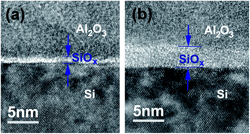 | ||
| Fig. 45 TEM images of Al2O3/Si interfaces (a) in the as-deposited state; and (b) after 550 °C rapid thermal annealing. Reproduced with permission from ref. 286. Copyright 2011, AIP Publishing LLC. | ||
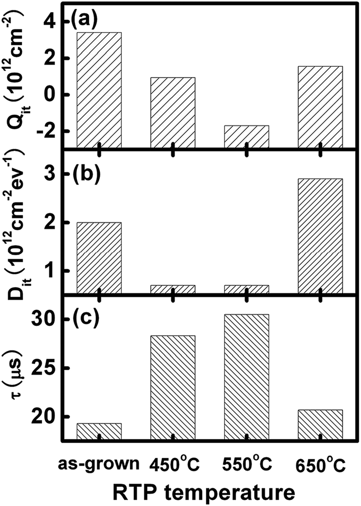 | ||
| Fig. 46 Evolution of (a) interfacial fixed charge density, Qit; (b) density of interfacial states, Dit; and (c) effective carrier lifetime, τ, for Al2O3 passivated p-Si wafers annealed at different temperatures via rapid thermal processing (RTP). Reproduced with permission from ref. 286. Copyright 2011, AIP Publishing LLC. | ||
The interfacial defect density between Al2O3 and Si is estimated to be ∼1011 eV−1 cm−2,265 which is higher than that offered by thermal oxide (109 to 1010 eV−1 cm−2). However, Al2O3 affords a stronger field effect passivation due to a larger Qf, up to ∼1013 cm−2.265,266,281 This value is much higher than that in SiO2, which amounts to ∼1010 to 1011 cm−2. Since the field effect passivation roughly scales with Qf2, it is about four orders of magnitude higher in Al2O3 than in thermal oxide; this effect relaxes the requirement on interfacial surface defects in Al2O3.265 Consequently, very low surface recombination velocity of 2 cm s−1 and 13 cm s−1 has been reported for low resistivity n-Si and p-Si wafers, respectively.266 These values are comparable to those offered by state-of-the-art thermal oxide passivation.
Al2O3 offers excellent surface passivation effects. A good level of passivation can be maintained down to ∼5 and ∼10 nm of Al2O3 for PE-ALD and thermal ALD, respectively.264 Owing to the negative built-in interfacial charge, Al2O3 is effective in passivating p-Si and has been used to passivate the rear surface of a n+/p solar cell.287 In cases of passivating p+-emitters, Al2O3 outperforms forming gas annealed thermal oxide, a-Si, and as-deposited a-SiNx265,288 and has been successfully incorporated on the emitter of a p+/n solar cell.289 Moreover, Black and co-workers have demonstrated that the passivation effects at the Si/Al2O3 interface are independent of the boron dopant concentration in the range from 9.2 × 10¹⁵ to 5.2 × 1019 cm−3.290
Because of its relatively low interfacial defect density (chemical passivation), Al2O3 has also been employed to passivate n+-emitters and offers good performance, although SiO2/Al2O3 stacks without negative charges are likely preferable.202,264,291
Similar to SiNx, Al2O3 (with a refractive index of ∼1.60–1.65 for 2 eV light266) can also serve as an AR layer. With 70 and 100 nm of Al2O3 coated on pyramidal structured silicon wafers, the averaged reflectance can be reduced from 14.2% to 4.2 and 2.8%, respectively.292
The ALD technique used for Al2O3 growth affords excellent thickness control, good step coverage and conformality, low defect density, high uniformity over a large area, good reproducibility, and low deposition temperature.202 Its properties are not affected by UV-radiation.281 Since the solar cell industry is predicted to shift to n-type silicon photovoltaics (with p+-emitters) soon, due to their relative insensitivity to various impurities and defects compared to p-type solar cells, Al2O3 is likely to play a more important role in this industry with its particular strengths in passivating p+-emitters and affording favourable optical properties.
The primary drawback of ALD Al2O3 is related to its slow growth rate, which renders an Al2O3 film thickness of ∼0.5–1.5 Å per cycle, at several seconds per cycle. To address this concern, several industrial processes have been developed.264 One method relies on batch-ALD, during which multiple wafers are processed simultaneously, and a throughput rate of >3000 solar cells per hour has been realized. Experimental results show that the passivation effect from industrial-scale ALD processes is comparable to those obtained at a wafer scale.
ALD Al2O3 is an attractive BSi passivation option, owing to its excellent conformality on nanostructures (Fig. 47) and has been investigated by several research groups.202,220,228,240,293–295 Otto et al. fabricated three BSi samples, using RIE on low resistivity p-Si wafers, and passivated them with 100 nm ALD Al2O3 (Fig. 47).228 The heights of these nanostructures were 500, 600, and 1700 nm, respectively, affording aspect ratios of 3, 4 and 10. Otto and co-workers showed that good passivation, comparable to that on planar wafers, was realized on the optimized BSi with an intermediate aspect ratio (Fig. 48). A very low surface recombination velocity, less than 13 cm s−1, has been measured, leading to an effective carrier lifetime in the ms range. The relatively poor performance of the other two BSi samples is likely caused by ion-induced surface damages during RIE, which was not thoroughly cleaned.
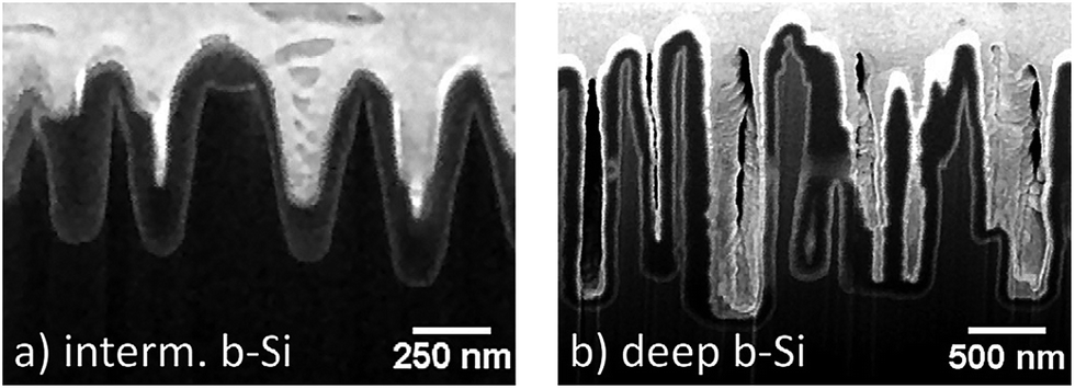 | ||
| Fig. 47 SEM images of BSi samples coated by ∼100 nm ALD Al2O3 (dark grey). A protection Pt film (white) is deposited before the cross-section preparation. Reproduced with permission from ref. 228. Copyright 2012, AIP Publishing LLC. | ||
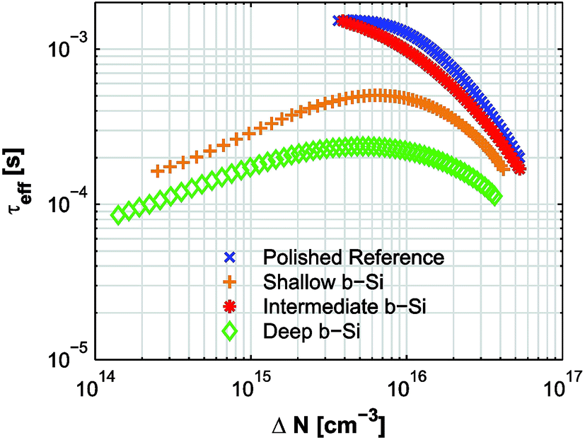 | ||
| Fig. 48 Injection level dependent carrier lifetime of three BSi samples with different aspect ratios and a reference planar wafer. All samples are passivated with 100 nm Al2O3, and annealed in low-pressure Ar ambient at 425 °C for 30 min. Reproduced with permission from ref. 228. Copyright 2012, AIP Publishing LLC. | ||
In another independent study on low-resistivity p-Si wafers, Repo et al. confirmed that the lifetime of BSi was in the ms range and comparable to that of planar wafers with ALD Al2O3 passivation.294 Repo and co-workers also noticed that the lifetime of Al2O3 passivated wafers was one order of magnitude longer than that with thermal oxide passivation. In addition to the good passivation properties, both Al2O3 and thermal oxide further improved the reflectance of BSi, down to less than 1%; and Al2O3 offered a slightly better optical performance than thermal oxide. This difference was attributed to two factors: their refractive indices are different; and the nanostructure morphologies may be changed slightly during thermal oxidation.294,295
Based on ALD Al2O3 passivation, Repo et al. fabricated an n-type PERL (passivated emitter with rear locally diffused) cell with BSi on the front p+-emitter side. This solar cell demonstrated a record high efficiency of 18.7%.220
ALD Al2O3 passivation has also been applied to a p-type BSi solar cell with an n+-emitter by Wang et al.202 In their case, good chemical passivation improved the carrier lifetime from 1.05 μs to 18.1 μS, leading to a high power conversion efficiency of 18.2%.
4.5. Stacked layers
Every dielectric passivation material has limitations. For example, the positive fixed charge in SiNx degrades its passivation effect on a p+-emitter; and the performance of Al2O3 is less ideal on an n+-emitter. A stacked dielectric layer, however, can be employed to avoid these drawbacks. For instance, a SiO2/Al2O3 stacked layer removes the negative fixed charge associated with Al2O3, and offers an improved passivation performance on n-Si.264In addition to tuning the fixed interfacial charge density, a stacked layer may also boost chemical passivation, such as in the case of SiO2/SiNx. In this stacked passivation layer, a SiO2 layer greater than 10 nm is required to provide a good interface to silicon; during the deposition of SiNx, further hydrogenation helps to passivate the dangling bonds at the Si/SiO2 interface, leading to an impressive passivation effect, comparable to that offered by the alneal process (Fig. 49).263 The SiO2/SiNx stack also greatly improves the thermal stability of the dielectric layer; this feature is critical for solar cell fabrication, since solar cells have to go through a few high temperature processes. Nevertheless, thermal oxide in this stacked layer is fabricated at high temperature and is not desirable.
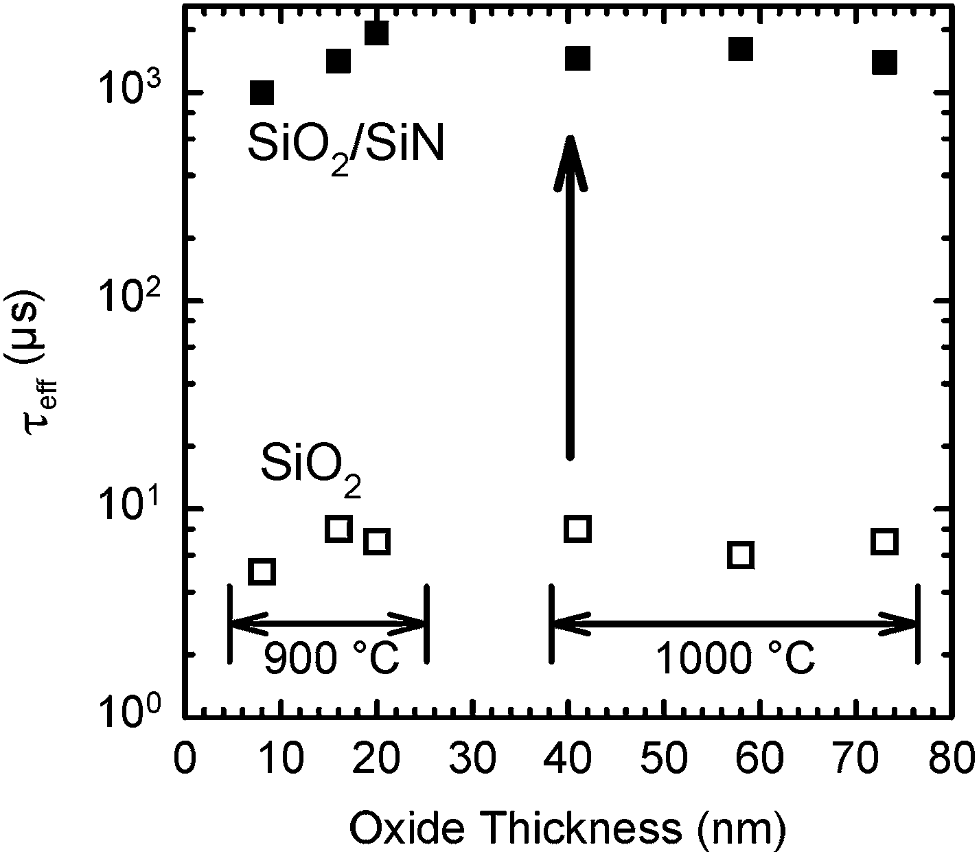 | ||
| Fig. 49 Comparison of the effective lifetime in a low resistivity p-Si wafer with only SiO2 passivation (open squares) and with a SiO2/SiNx stacked passivation layer. The SiO2 thickness varies according to the growth temperature (900 or 1000 °C) and growth time (5–63 min), while the thickness of SiNx is fixed at 60 nm.263 © IOP Publishing. Reproduced by permission of IOP Publishing. All rights reserved. | ||
To avoid high-temperature thermal oxide growth, Dingemans et al. used PECVD to grow a SiOx/SiNy stack and passivate a low resistivity p-Si wafer.296 They reported a low surface recombination velocity (<11 cm s−1). Duttagupta et al. further extended this technique to passivate a p+-emitter. They deposited a stack of 15 nm SiOx and 70 nm a-SiNx. Upon annealing, the interfacial fixed charge density amounts to ∼1011 cm−2 and the interface defect density is reduced to ∼3 × 10¹⁰ V−1 cm−2; consequently, a low J0e of ∼25 fA cm−2 was measured. This study shows that a modest positive fixed charge density of ∼1011 cm−2 can be tolerated for passivating p+ emitters in the presence of excellent chemical passivation.297 This stacked film also exhibits an AR effect, reducing the weighted reflectance in the range 300–1000 nm to ∼2%.
One potential concern for SiO2/SiNx stacked layers regards UV radiation induced damages. The defects at the Si/SiO2 interface can be created following the injection of energetic electrons from the silicon substrate to SiO2 under UV radiation. Typically, un-concentrated sunlight is not sufficiently energetic to cause such damage. However, with SiNx coating which introduces a positive charge density of ∼2 × 1012 cm−2, a defect can be created by a much lower energy photon, i.e., 3.95 eV (314 nm); such photons are abundantly available in the solar spectrum.298
Stacked Al2O3/SiNx layers have also been employed for both passivation and AR effects on p-Si. In particular, Al2O3 may be deposited by PECVD instead of ALD on planar wafers to minimize cost and increase throughput. Duttagupta et al. showed that in the PECVD AlOx/SiNy stacked layer on a p+ emitter, 5 nm AlOx was enough for the passivation effect; the additional 65 nm SiNx boosted AR effects and afforded a weighted reflectance of 2.3% in the range 300 to 1000 nm.299
When used in BSi solar cells, one additional concern on the dielectric passivation layer regards its surface conformality. SiO2/SiNx has thus been adopted by several research groups.207–209 SiO2 is preferred for its great surface conformality (Fig. 34). Liu et al. showed that SiNx could not completely cover the BSi surface, resulting in a solar cell efficiency of only 14.9% (Fig. 44a).207 By inserting an additional thermal oxide layer (20 nm) between bulk silicon and SiNx (60 nm), the surface coverage and associated passivation effect is greatly improved (Fig. 44b); consequently, the solar cell efficiency rises to 15.8%. Similarly, Zhao and co-workers found that their solar cell passivated by the stacked layer of SiO2/SiNx offers higher power conversion efficiency (17.1%), in comparison to those passivated either by SiO2 (16.1%) or SiNx (16.5%) alone.208 Interestingly, Zhao et al. also noticed that thermal oxidation reduces emitter doping concentration, which is beneficial for minimizing Auger recombination in an over-heavily doped emitter.208 However, high temperature thermal oxidation is undesirable, especially for mc-Si solar cells. Hsu et al. adopted a trade-off strategy by performing a quick thermal anneal followed by PECVD SiNx growth on an n+-emitter. With a hydrogenated SiO2 (5 nm)/SiNx (50 nm) stack, the minority carrier lifetime increased substantially from 1.8 to 7.2 μs for a 100 nm-long nano-rod coated solar cell and a high power conversion efficiency of 16.38% was measured.209 Instead of thermal oxide, Wong et al. passivated their nanostructured n+-emitter with 20 nm ALD Al2O3 to achieve good surface conformality, followed by 70 nm PECVD SiNx. A power conversion efficiency of 16.5% was achieved.211
5 Future research directions
5.1. Encapsulation effects
When solar cells are deployed in open-air fields or installed on rooftops, they are encapsulated under a glass layer to prevent moisture attack, mechanical damage and electrical shock. Encapsulation plays a critical role in the energy production and field performance of solar cells. Yet, it is largely ignored in BSi research when the performance of its different textures are evaluated. To our best knowledge, the only work taking encapsulation into consideration was that undertaken by Gjessing and Marstein (Fig. 50).300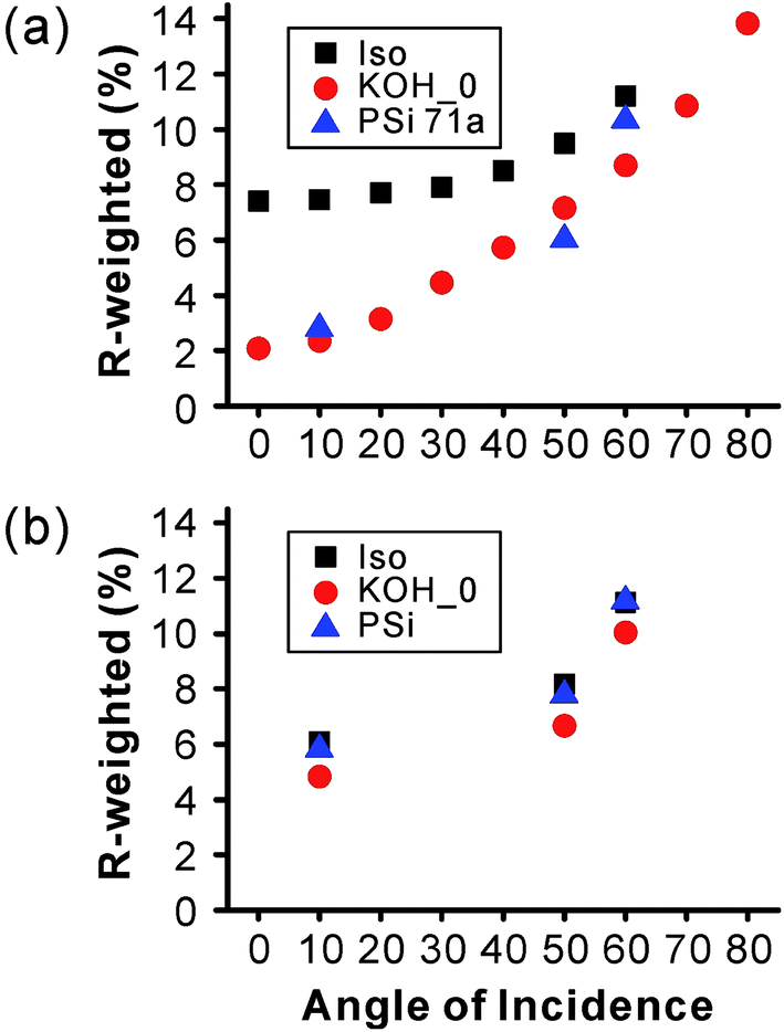 | ||
| Fig. 50 Weighted reflectance of c-Si with different surface textures via isotropic acid etching, KOH etching (pyramidal structures), and electrochemical HF etching (porous silicon) (a) before and (b) after glass encapsulation.300 Reproduced by permission of Elsevier. | ||
Gjessing and Marstein compared the weighted reflectance of three different textures on c-Si wafers, fabricated via isotropic acid etching, KOH etching (pyramidal structures), and electrochemical HF etching (porous silicon with gradient porosity), and calculated the weighted reflectance using the AM1.5 spectrum from 350 to 1200 nm.300 Note that the first two textures were further coated with a layer of SiNx ARC. Gjessing and Marstein's absolute reflectance readings are likely to be biased, owing to the use of partly polarized illumination and the potential mixing of reflections from both the front and rear sides of the wafers—especially in the long wavelength region. However, they demonstrated one important trend: the reflectance differences among different textures decreased from ∼5% to only ∼1% upon encapsulation.300
Essentially, the main effect of encapsulation is a change of the medium refractive index in the superstrate from n = 1 to n = 1.5. This effect reduces the AR requirement significantly, while having little impact on the requirement for improved light trapping. Good pyramidal and isotextured surfaces (combined with ARC) reach very low reflectance values and are, arguably, not much worse than BSi in air.
This result indicates that the encapsulation effect must be taken into account, when optimizing the surface roughness of BSi and balancing its optical and electrical gains for practical applications. To be more specific, since the optical gain of BSi relative to other textures is reduced upon encapsulation, a lower aspect ratio nanostructured surface might be required to optimize BSi solar cell efficiency.
5.2. Dual-scale structures
It is expected that dual-scale structures, in which nano-scaled structures are coated on micro-scaled textures, will play an increasingly important role in the development of BSi (>100 μm; Fig. 51). Both anti-reflection and light trapping/scattering are critical for increasing the optical path length and enhancing photon absorption in solar cells, especially for thin film silicon PV devices. However, sub-100 nm nanostructured BSi is equivalent to an effective index medium; it is optically flat and does not have significant scattering/trapping effects. In other words, this type of BSi offers excellent AR effects, but normal incident light will penetrate through this wafer without much absorption. Nevertheless, the light scattering/trapping effects can be addressed by combining microstructured texture with nanostructured surface. Second, the surface area in BSi must be controlled for a better electrical performance. However, adopting low aspect ratio nanostructures degrades the optical performance of BSi. In contrast, the dual-scale structure is an effective solution to balance the conflicting demands on the reflectance and surface area of BSi. It affords an equivalent optical performance with a reduced thickness or surface area of the nano-structured layer. Third, the microstructured surface improves the mechanical properties of BSi. Xiu et al. showed that the dual-scale structure remained non-wettable under abrasion, since nanostructures are protected by the relatively strong micro-structures.301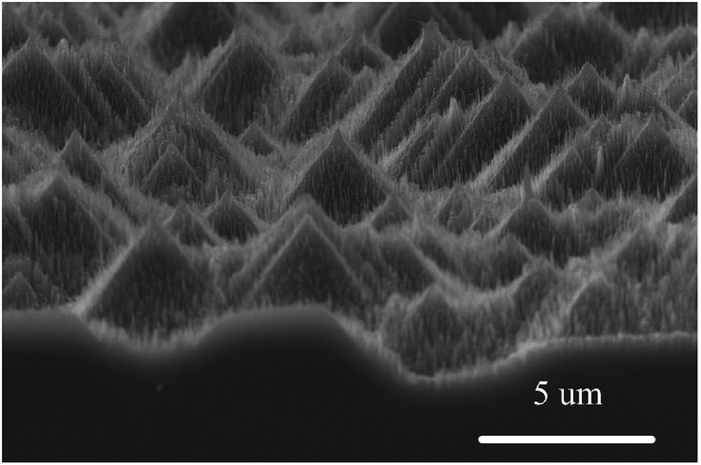 | ||
| Fig. 51 A micro- and nano-dual scale surface texture on a (100) wafer.224 Reproduced by permission of the Electrochemical Society. | ||
To this end, Toor et al. applied dual-scale texturization on a (100) silicon wafer.35 They first fabricated conventional pyramidal structures on the wafer, followed by producing a thin layer of nanostructured surface using metal-catalyzed chemical etching. Consequently, the weighted reflectance (from 350 to 1000 nm) of 1.8% is realized with a nanostructured layer that is only 100 nm thick, in contrast to ∼250 nm on a planar BSi for the same reflectance. This light management strategy minimizes the surface area without compromising the antireflection benefits. The thinner nanostructured layer also improves the blue response of the BSi solar cell, leading to a 17.1% power conversion efficiency. Similar dual-scale surface texture strategies have also been used by several other research groups, where the nanostructured layers are fabricated via different techniques, such as metal-assisted chemical etching, electrochemical HF etching, and modified RIE etching.35,36,41,208,211–213,217,224,302,303
The dual-scale structure can be potentially fabricated in a single fabrication step. Vorobyev and Guo produced a parallel micro-grooved silicon surface structure by scanning a fs-laser through a wafer.304 Fine-micro and nanostructures are imposed on top of the ridges and valleys of these groove-structures (Fig. 52). This dual-level structure demonstrates a low reflectance across a broadband. In the visible range (250–1000 nm), the reflectance is ∼3–4%; in the mid-IR region, the reflectance increases to ∼20% but still amounts to only half of that on an untreated surface. This BSi displays remarkable mechanical strength, unlike other nanostructured surfaces. However, the absorption in the above-bandgap region clearly indicates the presence of laser-induced defects; annealing and/or etching to remove defects is necessary where electrical performance is of great concern.
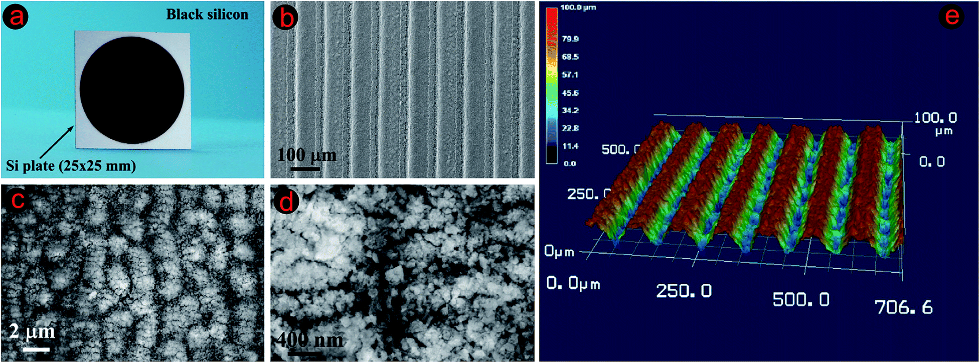 | ||
| Fig. 52 (a) A photography of laser treated BSi; (b) SEM image of the micro-grooved BSi; (c) and (d) correspond to the zoomed-in SEM images, showing the micro- and nano-scale surface texture, respectively; (d) A 3D optical image of the micro-grooved BSi.304 Adapted by permission of Elsevier. | ||
Interestingly, the “dual-scale design” can also be realized by structuring both the front and back surfaces of a silicon substrate, for anti-reflection and light trapping, respectively. With optimized structures, photocurrent close to the Yablonovitch limit was predicted for thin film silicon solar cells.188,305
5.3. Thin solar cells
One possible route to reduce the cost of silicon photovoltaics is to develop thin film solar cells (thickness < 30 μm) or even ultra-thin solar cells (thickness < 10 μm), by significantly decreasing the consumption of silicon during solar cell fabrication. Thin solar cells also offer many other advantages, such as light weight, mechanical flexibility, and easy integration with a diverse range of substrate materials.186,306–308 Surface texture of ultra-thin silicon via alkaline or acid wet etching requires the usage of a photolithography-defined mask309 and is not considered to be industrially compatible.233 Hence, the limitation of wet etching in thin film silicon solar cells presents a good opportunity for developing BSi texture.While BSi poses several challenges, such as in preforming doping, forming good Si/metal contact and increasing surface recombination, novel cell designs can be adopted to mitigate these problems. For example, in a back-contact back-junction (BCBJ) solar cell, the active junction is formed at the rear side and the interdigitated metal contact is built on a flat substrate surface (Fig. 53a). The BCBJ design has been used in thick silicon solar cells;310–313 Jeong et al. have showed that the benefits of this design are even more significant in thin solar cells, avoiding the doping and contact formation problems associated with BSi. Consequently, a power conversion efficiency of 13.7% was realized in an ultrathin solar cell (thickness < 10 μm); cf. 10.9% in a planar solar cell with ARC.314
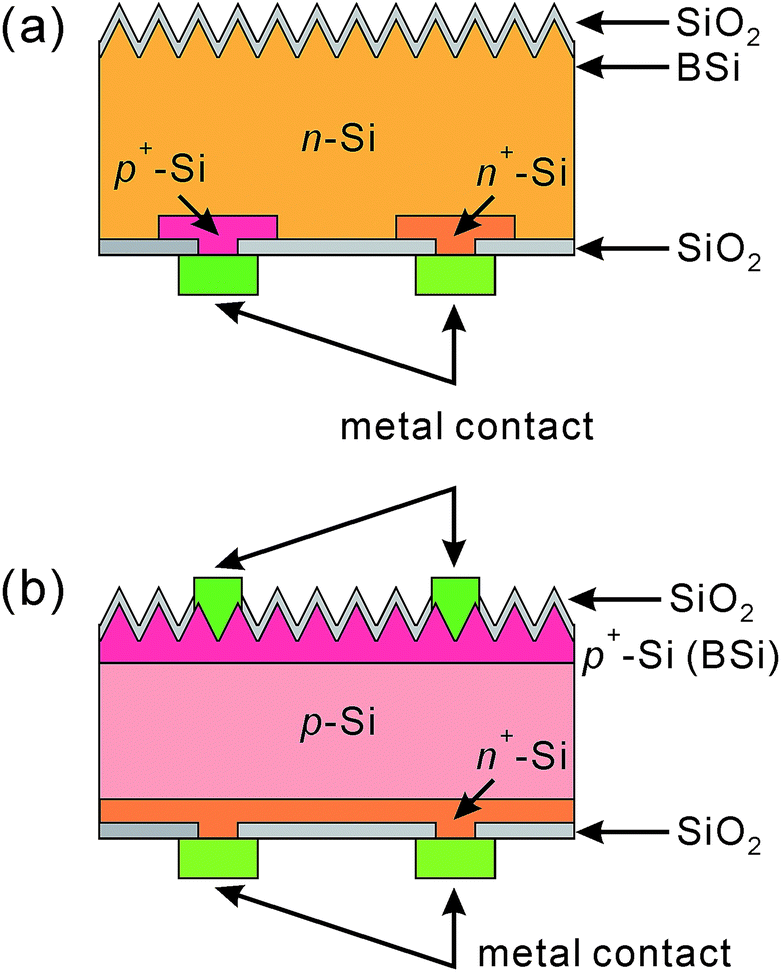 | ||
| Fig. 53 (a) A schematic of a back-contact back-junction solar cell with a BSi front surface.314 (b) A schematic of a back-junction solar cell with a BSi front surface and front surface field.187 | ||
In another slightly different design (Fig. 53b), the p–n junction is also formed at the flat rear side, while the front metal contact is still built on BSi. However, a front surface field (FSF) has been created via heavy boron doping, in order to reduce surface recombination. A similar design has been adopted by Chan and co-workers in fabricating ∼5.7 μm thick micro-BSi solar cells.187 It should be pointed that a FSF may also be incorporated into a BCBJ cell. In addition to its role of reducing surface recombination, a FSF also improves lateral base conductivity and enhances cell stability against UV radiation in BCBJ solar cells.315–317
For thin solar cells, light trapping becomes critical for photon management, in addition to anti-reflection.318–322 BSi with a feature size less than 100 nm is optically flat and does not scatter light nor increase the optical path length. Hence, additional light trapping structures become essential to enhance the efficiencies of this type of thin solar cell. By incorporating a diffuse backside reflector into a BSi microcell, Chan et al. have showed that the solar cell efficiency improved from 6.9% to 11.4%.187 Alternatively, one may also consider optimizing the feature size of BSi; optimal modeling has showed that a sub-microstructured surface (with period > ∼500 nm) could retain good light trapping effects, while simultaneously maintaining low surface reflection.234
6 Concluding remarks
Various methods have been developed to fabricate micro- or nano-structured BSi surfaces. By carefully varying their process parameters, a wide range of surface morphologies can be created with a high degree of control. For example, the porosity and thickness can be manipulated by simply adjusting current density and etching time during electrochemical etching in HF. Moreover, the wet etching, such as metal-assisted chemical etching, holds a great promise for large scale industrial deployment, owing to its simple experimental setup and fast etching rate. We should also highlight RIE, which can produce silicon nano-needles and result in smooth refractive index transitions from air to bulk silicon. Consequently, very low reflectance, down to less than 1% over a broadband and different polarization, has been realized with BSi.While BSi offers superior optical performance, its poor electrical characteristics hinder the overall power conversion efficiencies of BSi solar cells. The roughed surface in BSi leads to increased surface recombination, causes high and sometimes non-uniform doping concentrations, and poses significant challenges for forming a good silicon/metal contact. Consequently, improved fabrication processes are required to balance the optical gains and electrical losses of BSi in order to achieve high solar cell efficiencies. A few strategies have thus been identified, including controlling the thickness of the nanostructured layer and using low aspect ratio nanostructures, developing new doping methods and minimizing Auger recombination, applying a thorough surface defect cleaning process and providing excellent surface passivation. The incorporation of BSi in advanced solar cell designs and in thin silicon wafer production has also been surveyed; these techniques may potentially improve solar cell efficiencies or reduce material cost during photovoltaic production. It is worth adding that BSi texturing methods are likely to also play an important role in mc-Si and ultra-thin solar cells—especially where conventional wet etching methods fail as cell thicknesses decrease.
Owing to the importance of surface passivation to BSi, major passivation techniques using SiNx, thermal oxide, Al2O3 and a-Si have been critically examined. It is found that atomic layer deposited Al2O3 offers excellent surface conformality and passivation to the silicon surface, especially on p+-emitters. With ALD Al2O3 passivation, a record high 18.7% efficient BSi solar cell has been successfully fabricated. As the market share of n-type solar cells (with p+-emitters) is expected to rise in the near future, this passivation technique is particularly attractive and may become a new industry standard.
While the efficiencies of BSi solar cells currently remain below those of conventional silicon solar cells, this review offers some promising solutions. In particular, with a better understanding of the carrier loss mechanisms and improvements in cell design and fabrication strategies, the efficiency of BSi solar cells will continue to increase. The future of BSi remains bright.
Acknowledgements
The Solar Energy Research Institute of Singapore is sponsored by the National University of Singapore (NUS) and the National Research Foundation of Singapore through the Singapore Economic Development Board (SEDB). X.L. is grateful to SEDB for a Clean Energy Scholarship. J.M.C. thanks the Fulbright Commission for a UK-US Fulbright Scholar Award, hosted by Argonne National Laboratory where work done was supported by DOE Office of Science, Office of Basic Energy Sciences, under contract no. DE-AC02-06CH11357. P.R.C. is indebted to I. Wender (Terrativa Minerais S.A.) for sponsoring this research.References
- H. Föll, M. Christophersen, J. Carstensen and G. Hasse, Mater. Sci. Eng., R, 2002, 39, 93–141 CrossRef.
- M. J. Sailor, Porous Silicon in Practice: Preparation, Characterization and Applications, Wiley, Weinheim, Germany, 2012 Search PubMed.
- K. W. Kolasinski, Curr. Opin. Solid State Mater. Sci., 2005, 9, 73–83 CrossRef CAS PubMed.
- G. Barillaro, A. Nannini and M. Piotto, Sens. Actuators, A, 2002, 102, 195–201 CrossRef CAS.
- A. Jane, R. Dronov, A. Hodges and N. H. Voelcker, Trends Biotechnol., 2009, 27, 230–239 CrossRef CAS PubMed.
- M. P. Stewart and J. Buriak, Adv. Mater., 2000, 12, 859–869 CrossRef CAS.
- L. De Stefano, L. Moretti, A. Lamberti, O. Longo, M. Rocchia, A. M. Rossi, P. Arcari and I. Rendina, IEEE Trans. Nanotechnol., 2004, 3, 49–54 CrossRef.
- A. Angelescu, I. Kleps, M. Mihaela, M. Simion, T. Neghina, S. Petrescu, N. Moldovan, C. Paduraru and A. Raducanu, Rev. Adv. Mater. Sci., 2003, 5, 440–449 Search PubMed.
- M. J. Sailor and E. J. Lee, Adv. Mater., 1997, 9, 783–793 CrossRef CAS PubMed.
- M. Berger, C. Dieker, M. Thonissen, L. Vescan, H. Luth, H. Munder, W. Theiss, M. Wernke and P. Grosse, J. Phys. D: Appl. Phys., 1994, 27, 1333–1336 CrossRef CAS.
- C. Mazzoleni and L. Pavesi, Appl. Phys. Lett., 1995, 67, 2983–2985 CrossRef CAS PubMed.
- M. Berger, M. Thönissen, R. Arens-Fischer, H. Münder, H. Lüth, M. Arntzen and W. Theiβ, Thin Solid Films, 1995, 255, 313–316 CrossRef CAS.
- M. Araki, H. Koyama and N. Koshida, Appl. Phys. Lett., 1996, 69, 2956–2958 CrossRef CAS PubMed.
- L. Pavesi, C. Mazzoleni, A. Tredicucci and V. Pellegrini, Appl. Phys. Lett., 1995, 67, 3280–3282 CrossRef CAS PubMed.
- M. Berger, R. Arens-Fischer, M. Thönissen, M. Krüger, S. Billat, H. Lüth, S. Hilbrich, W. Theiss and P. Grosse, Thin Solid Films, 1997, 297, 237–240 CrossRef CAS.
- V. Torres-Costa and R. J. Martín-Palma, J. Mater. Sci., 2010, 45, 2823–2838 CrossRef CAS.
- M. Steglich, M. Zilk, F. Schrempel, A. Tünnermann and E. B. Kley, Appl. Phys. Lett., 2013, 102, 111110 CrossRef PubMed.
- M. Steglich, M. Zilk, A. Bingel, C. Patzig, T. Käsebier, F. Schrempel, E.-B. Kley and A. Tünnermann, J. Appl. Phys., 2013, 114, 183102 CrossRef PubMed.
- J.-H. Park, L. Gu, G. von Maltzahn, E. Ruoslahti, S. N. Bhatia and M. J. Sailor, Nat. Mater., 2009, 8, 331–336 CrossRef CAS PubMed.
- J. Rong, C. Masarapu, J. Ni, Z. Zhang and B. Wei, ACS Nano, 2010, 4, 4683–4690 CrossRef CAS PubMed.
- M. Ge, X. Fang, J. Rong and C. Zhou, Nanotechnology, 2013, 24, 422001 CrossRef CAS PubMed.
- A. Vu, Y. Qian and A. Stein, Adv. Energy Mater., 2012, 2, 1056–1085 CrossRef CAS PubMed.
- J. Oh, T. G. Deutsch, H.-C. Yuan and H. M. Branz, Energy Environ. Sci., 2011, 4, 1690–1694 CAS.
- E. P. Ivanova, J. Hasan, H. K. Webb, G. Gervinskas, S. Juodkazis, V. K. Truong, A. H. Wu, R. N. Lamb, V. A. Baulin and G. S. Watson, Nat. Commun., 2013, 4, 2838 Search PubMed.
- D. Qi, N. Lu, H. Xu, B. Yang, C. Huang, M. Xu, L. Gao, Z. Wang and L. Chi, Langmuir, 2009, 25, 7769–7772 CrossRef CAS PubMed.
- M. Barberoglou, V. Zorba, A. Pagozidis, C. Fotakis and E. Stratakis, Langmuir, 2010, 26, 13007–13014 CrossRef CAS PubMed.
- P. Granitzer and K. Rumpf, Materials, 2010, 3, 943–998 CrossRef CAS PubMed.
- A. B. Christiansen, J. S. Clausen, N. A. Mortensen and A. Kristensen, Microelectron. Eng., 2014, 121, 47–50 CrossRef PubMed.
- J. Wei, J. M. Buriak and G. Siuzdak, Nature, 1999, 399, 243–246 CrossRef CAS PubMed.
- S. Fan, M. G. Chapline, N. R. Franklin, T. W. Tombler, A. M. Cassell and H. Dai, Science, 1999, 283, 512–514 CrossRef CAS.
- A. Žukauskas, M. Malinauskas, A. Kadys, G. Gervinskas, G. Seniutinas, S. Kandasamy and S. Juodkazis, Opt. Express, 2013, 21, 6901–6909 CrossRef PubMed.
- J. Oh, H. C. Yuan and H. M. Branz, Nat. Nanotechnol., 2012, 7, 743–748 CrossRef CAS PubMed.
- Y. Wang, Y. P. Liu, T. Lai, H. L. Liang, Z. L. Li, Z. X. Mei, F. M. Zhang, A. Kuznetsov and X. L. Du, RSC Adv., 2013, 3, 15483–15489 RSC.
- H. C. Yuan, V. E. Yost, M. R. Page, P. Stradins, D. L. Meier and H. M. Branz, Appl. Phys. Lett., 2009, 95, 123501 CrossRef PubMed.
- F. Toor, H. M. Branz, M. R. Page, K. M. Jones and H. C. Yuan, Appl. Phys. Lett., 2011, 99, 103501 CrossRef PubMed.
- X. Ao, X. Tong, D. S. Kim, L. Zhang, M. Knez, F. Müller, S. He and V. Schmidt, Appl. Phys. Lett., 2012, 101, 111901 CrossRef PubMed.
- G. Masson, M. Latour, M. Rekinger, I. Theologitis and M. Papoutsi, Global Market Outlook for Photovoltaics 2013–2017, European Photovoltaic Industry Association, 2013 Search PubMed.
- P. Menna, G. Di Francia and V. La Ferrara, Sol. Energy Mater. Sol. Cells, 1995, 37, 13–24 CrossRef CAS.
- L. Stalmans, J. Poortmans, H. Bender, M. Caymax, K. Said, E. Vazsonyi, J. Nijs and R. Mertens, Prog. Photovolt. Res. Appl., 1998, 6, 233–246 CrossRef CAS.
- V. Y. Yerokhov and I. I. Melnyk, Renewable Sustainable Energy Rev., 1999, 3, 291–322 CrossRef CAS.
- R. Bilyalov, R. Lüdemann, W. Wettling, L. Stalmans, J. Poortmans, J. Nijs, L. Schirone, G. Sotgiu, S. Strehlke and C. Lévy-Clément, Sol. Energy Mater. Sol. Cells, 2000, 60, 391–420 CrossRef CAS.
- M. D. Kelzenberg, S. W. Boettcher, J. A. Petykiewicz, D. B. Turner-Evans, M. C. Putnam, E. L. Warren, J. M. Spurgeon, R. M. Briggs, N. S. Lewis and H. A. Atwater, Nat. Mater., 2010, 9, 239–244 CrossRef CAS.
- C. L. Cheng, C. W. Liu, J. T. Jeng, B. T. Dai and Y. H. Lee, J. Electrochem. Soc., 2009, 156, H356–H360 CrossRef CAS PubMed.
- L. Tsakalakos, J. Balch, J. Fronheiser, B. Korevaar, O. Sulima and J. Rand, Appl. Phys. Lett., 2007, 91, 233117 CrossRef PubMed.
- Y. Li, H. Yu, J. Li, S. M. Wong, X. W. Sun, X. Li, C. Cheng, H. J. Fan, J. Wang and N. Singh, Small, 2011, 7, 3138–3143 CrossRef CAS PubMed.
- S. Chattopadhyay, Y. F. Huang, Y. J. Jen, A. Ganguly, K. H. Chen and L. C. Chen, Mater. Sci. Eng., R, 2010, 69, 1–35 CrossRef PubMed.
- R. Memming and G. Schwandt, Surf. Sci., 1966, 4, 109–124 CrossRef CAS.
- A. Cullis and L. Canham, Nature, 1991, 353, 335–338 CrossRef CAS.
- A. Cullis, L. T. Canham and P. Calcott, J. Appl. Phys., 1997, 82, 909–965 CrossRef CAS PubMed.
- K. Hirschman, L. Tsybeskov, S. Duttagupta and P. Fauchet, Nature, 1996, 384, 338–341 CrossRef CAS.
- L. T. Canham, Appl. Phys. Lett., 1990, 57, 1046–1048 CrossRef CAS PubMed.
- L. H. Lie, M. Duerdin, E. M. Tuite, A. Houlton and B. R. Horrocks, J. Electroanal. Chem., 2002, 538, 183–190 CrossRef.
- Y. Chao, L. Šiller, S. Krishnamurthy, P. R. Coxon, U. Bangert, M. Gass, L. Kjeldgaard, S. N. Patole, L. H. Lie and N. O'Farrell, Nat. Nanotechnol., 2007, 2, 486–489 CrossRef PubMed.
- J. H. Ahire, Q. Wang, P. R. Coxon, G. Malhotra, R. Brydson, R. Chen and Y. Chao, ACS Appl. Mater. Interfaces, 2012, 4, 3285–3292 CAS.
- P. Kleimann, J. Linnros and R. Juhasz, Appl. Phys. Lett., 2001, 79, 1727–1729 CrossRef CAS PubMed.
- H. S. Jang, H.-J. Choi, B.-Y. Oh and J. H. Kim, Electrochem. Solid-State Lett., 2011, 14, D5–D9 CrossRef CAS PubMed.
- X. Zhang, S. Collins and R. Smith, J. Electrochem. Soc., 1989, 136, 1561–1565 CrossRef CAS PubMed.
- X. Zhang, J. Electrochem. Soc., 2004, 151, C69–C80 CrossRef CAS PubMed.
- P. Kleimann, X. Badel and J. Linnros, Appl. Phys. Lett., 2005, 86, 183108 CrossRef PubMed.
- V. Lehmann, Electrochemistry of Silicon: Instrumantation, Science, Materials and Applications, Wiley-VCH, Weinheim, 2002 Search PubMed.
- S. Matthias, F. MüLLER, C. Jamois, R. B. Wehrspohn and U. Gösele, Adv. Mater., 2004, 16, 2166–2170 CrossRef CAS PubMed.
- C. Striemer and P. Fauchet, Appl. Phys. Lett., 2002, 81, 2980–2982 CrossRef CAS PubMed.
- R. Bilyalov, L. Stalmans and J. Poortmans, J. Electrochem. Soc., 2003, 150, G216–G222 CrossRef CAS PubMed.
- L. L. Ma, Y. C. Zhou, N. Jiang, X. Lu, J. Shao, W. Lu, J. Ge, X. M. Ding and X. Y. Hou, Appl. Phys. Lett., 2006, 88, 171907 CrossRef PubMed.
- D. Ariza-Flores, J. Pérez-Huerta, Y. Kumar, A. Encinas and V. Agarwal, Sol. Energy Mater. Sol. Cells, 2014, 123, 144–149 CrossRef CAS PubMed.
- E. Osorio, R. Urteaga, L. N. Acquaroli, G. García-Salgado, H. Juaréz and R. R. Koropecki, Sol. Energy Mater. Sol. Cells, 2011, 95, 3069–3073 CrossRef CAS PubMed.
- H. A. Macleod, Thin-Film Optical Filters, CRC Press, Boca Raton, FL, 4th edn, 2010 Search PubMed.
- J. H. Selj, T. T. Mongstad, R. Søndenå and E. S. Marstein, Sol. Energy Mater. Sol. Cells, 2011, 95, 2576–2582 CrossRef CAS PubMed.
- V. Y. Yerokhov, R. Hezel, M. Lipinski, R. Ciach, H. Nagel, A. Mylyanych and P. Panek, Sol. Energy Mater. Sol. Cells, 2002, 72, 291–298 CrossRef CAS.
- SEMSYSCO, http://www.semsysco.com/porous-silicon/, accessed June 30 2014.
- R. Smith and S. Collins, J. Appl. Phys., 1992, 71, R1–R22 CrossRef CAS PubMed.
- S. Shih, K. Jung, T. Hsieh, J. Sarathy, J. Campbell and D. Kwong, Appl. Phys. Lett., 1992, 60, 1863–1865 CrossRef CAS PubMed.
- H. Robbins and B. Schwartz, J. Electrochem. Soc., 1959, 106, 505–508 CrossRef CAS PubMed.
- H. Robbins and B. Schwartz, J. Electrochem. Soc., 1960, 107, 108–111 CrossRef CAS PubMed.
- B. Schwartz and H. Robbins, J. Electrochem. Soc., 1961, 108, 365–372 CrossRef CAS PubMed.
- B. Schwartz and H. Robbins, J. Electrochem. Soc., 1976, 123, 1903–1909 CrossRef CAS PubMed.
- É. Vázsonyi, E. Szilágyi, P. Petrik, Z. Horváth, T. Lohner, M. Fried and G. Jalsovszky, Thin Solid Films, 2001, 388, 295–302 CrossRef.
- G. Kumaravelu, M. M. Alkaisi, A. Bittar, D. Macdonald and J. Zhao, Curr. Appl. Phys., 2004, 4, 108–110 CrossRef PubMed.
- R. Khandelwal, U. Plachetka, B. Min, C. Moormann and H. Kurz, Microelectron. Eng., 2013, 111, 220–223 CrossRef CAS PubMed.
- Y.-T. Cheng, J.-J. Ho, S.-Y. Tsai, Z.-Z. Ye, W. Lee, D.-S. Hwang, S.-H. Chang, C.-C. Chang and K. L. Wang, Sol. Energy, 2011, 85, 87–94 CrossRef CAS PubMed.
- D. Turner, J. Electrochem. Soc., 1960, 107, 810–816 CrossRef CAS PubMed.
- M. Winton, S. Russell and R. Gronsky, J. Appl. Phys., 1997, 82, 436–441 CrossRef CAS PubMed.
- M. Saadoun, N. Mliki, H. Kaabi, K. Daoudi, B. Bessaıs, H. Ezzaouia and R. Bennaceur, Thin Solid Films, 2002, 405, 29–34 CrossRef CAS.
- M. B. Rabha, W. Dimassi, M. Bouaïcha, H. Ezzaouia and B. Bessais, Sol. Energy, 2009, 83, 721–725 CrossRef PubMed.
- M. Ben Rabha, M. Saadoun, M. Boujmil, B. Bessais, H. Ezzaouia and R. Bennaceur, Appl. Surf. Sci., 2005, 252, 488–493 CrossRef CAS PubMed.
- A. Ben Jaballah, M. Hassen, M. Hajji, M. Saadoun, B. Bessais and H. Ezzaouia, Phys. Status Solidi A, 2005, 202, 1606–1610 CrossRef CAS PubMed.
- A. B. Jaballah, M. Saadoun, M. Hajji, H. Ezzaouia and B. Bessaïs, Appl. Surf. Sci., 2004, 238, 199–203 CrossRef PubMed.
- M. Saadoun, B. Bessaïs, N. Mliki, M. Ferid, H. Ezzaouia and R. Bennaceur, Appl. Surf. Sci., 2003, 210, 240–248 CrossRef CAS.
- M. B. Rabha, H. Anouar and B. Brahim, Sol. Energy, 2012, 86, 1411–1415 CrossRef PubMed.
- R. T. Collins, P. M. Fauchet and M. A. Tischler, Phys. Today, 1997, 50, 24–31 CrossRef CAS PubMed.
- X. Li and P. Bohn, Appl. Phys. Lett., 2000, 77, 2572–2574 CrossRef CAS PubMed.
- Z. Huang, N. Geyer, P. Werner, J. De Boor and U. Gösele, Adv. Mater., 2011, 23, 285–308 CrossRef CAS PubMed.
- K. Nishioka, S. Horita, K. Ohdaira and H. Matsumura, Sol. Energy Mater. Sol. Cells, 2008, 92, 919–922 CrossRef CAS PubMed.
- S. Yae, Y. Kawamoto, H. Tanaka, N. Fukumuro and H. Matsuda, Electrochem. Commun., 2003, 5, 632–636 CrossRef CAS.
- S. K. Srivastava, D. Kumar, P. K. Singh, M. Kar, V. Kumar and M. Husain, Sol. Energy Mater. Sol. Cells, 2010, 94, 1506–1511 CrossRef CAS PubMed.
- S. Koynov, M. S. Brandt and M. Stutzmann, Appl. Phys. Lett., 2006, 88, 203107 CrossRef PubMed.
- Y. T. Lu and A. R. Barron, Phys. Chem. Chem. Phys., 2013, 15, 9862–9870 RSC.
- C. Y. Chen, W. J. Li and H. H. Chen, ChemPhysChem, 2012, 13, 1415–1420 CrossRef CAS PubMed.
- Y. Li, J. Zhang, S. Zhu, H. Dong, Z. Wang, Z. Sun, J. Guo and B. Yang, J. Mater. Chem., 2009, 19, 1806–1810 RSC.
- W. Choi, T. Liew, M. Dawood, H. I. Smith, C. Thompson and M. Hong, Nano Lett., 2008, 8, 3799–3802 CrossRef CAS PubMed.
- S. W. Chang, V. P. Chuang, S. T. Boles, C. A. Ross and C. V. Thompson, Adv. Funct. Mater., 2009, 19, 2495–2500 CrossRef CAS PubMed.
- C. F. Guo, T. Sun, Y. Wang, J. Gao, Q. Liu, K. Kempa and Z. Ren, Small, 2013, 9, 2415–2419 CrossRef CAS PubMed.
- Y. Matsui and S. Adachi, J. Appl. Phys., 2013, 113, 173502 CrossRef PubMed.
- S. Koynov, M. S. Brandt and M. Stutzmann, J. Appl. Phys., 2011, 110, 043537 CrossRef PubMed.
- S. K. Srivastava, D. Kumar, M. Sharma, R. Kumar and P. K. Singh, Sol. Energy Mater. Sol. Cells, 2012, 100, 33–38 CrossRef CAS PubMed.
- H. Jansen, M. de Boer, R. Legtenberg and M. Elwenspoek, J. Micromech. Microeng., 1995, 5, 115–120 CrossRef CAS.
- R. Dussart, T. Tillocher, P. Lefaucheux and M. Boufnichel, J. Phys. D: Appl. Phys., 2014, 47, 123001 CrossRef.
- R. Dussart, M. Boufnichel, G. Marcos, P. Lefaucheux, A. Basillais, R. Benoit, T. Tillocher, X. Mellhaoui, H. Estrade-Szwarckopf and P. Ranson, J. Micromech. Microeng., 2004, 14, 190 CrossRef CAS.
- R. Dussart, X. Mellhaoui, T. Tillocher, P. Lefaucheux, M. Boufnichel and P. Ranson, Microelectron. Eng., 2007, 84, 1128–1131 CrossRef CAS PubMed.
- R. Dussart, X. Mellhaoui, T. Tillocher, P. Lefaucheux, M. Volatier, C. Socquet-Clerc, P. Brault and P. Ranson, J. Phys. D: Appl. Phys., 2005, 38, 3395 CrossRef CAS.
- M. J. De Boer, J. G. E. Gardeniers, H. V. Jansen, E. Smulders, M. J. Gilde, G. Roelofs, J. N. Sasserath and M. Elwenspoek, J. Microelectromech. Syst., 2002, 11, 385–401 CrossRef CAS.
- H. V. Jansen, M. J. De Boer, S. Unnikrishnan, M. C. Louwerse and M. C. Elwenspoek, J. Micromech. Microeng., 2009, 19, 033001 CrossRef.
- X. Mellhaoui, R. Dussart, T. Tillocher, P. Lefaucheux, P. Ranson, M. Boufnichel and L. J. Overzet, J. Appl. Phys., 2005, 98, 104901 CrossRef PubMed.
- M. Kroll, M. Otto, T. KŠsebier, K. Füchsel, R. Wehrspohn, E. B. Kley, A. Tunnermann and T. Pertsch, Proceedings of Photonics for Solar Energy Systems IV, Brussels, 2012, p. 843817 Search PubMed.
- J. Yoo, G. Yu and J. Yi, Mater. Sci. Eng., B, 2009, 159–160, 333–337 CrossRef CAS PubMed.
- J. S. Yoo, I. O. Parm, U. Gangopadhyay, K. Kim, S. K. Dhungel, D. Mangalaraj and J. Yi, Sol. Energy Mater. Sol. Cells, 2006, 90, 3085–3093 CrossRef CAS PubMed.
- S. M. Rossnagel, J. J. Cuomo and W. D. Westwood, Handbook of Plasma Processing Technology: Fundamentals, Etching, Deposition, and Surface Interactions, William Andrew Inc., Norwich, New York, 1990 Search PubMed.
- Y. Xia, B. Liu, S. Zhong and C. Li, J. Electron Spectrosc. Relat. Phenom., 2012, 184, 589–592 CrossRef CAS PubMed.
- Y. Xia, B. Liu, J. Liu, Z. Shen and C. Li, Sol. Energy, 2011, 85, 1574–1578 CrossRef CAS PubMed.
- N. Cheung, Mater. Chem. Phys., 1996, 46, 132–139 CrossRef CAS.
- D. Murias, C. Reyes-Betanzo, M. Moreno, A. Torres, A. Itzmoyotl, R. Ambrosio, M. Soriano, J. Lucas and P. R. I. Cabarrocas, Mater. Sci. Eng., B, 2012, 177, 1509–1513 CrossRef CAS PubMed.
- J. Gittleman, E. Sichel, H. Lehmann and R. Widmer, Appl. Phys. Lett., 1979, 35, 742–744 CrossRef CAS PubMed.
- Y. Inomata, K. Fukui and K. Shirasawa, Sol. Energy Mater. Sol. Cells, 1997, 48, 237–242 CrossRef CAS.
- J. Yoo, Sol. Energy, 2010, 84, 730–734 CrossRef CAS PubMed.
- S. Kalem, P. Werner, Ö. Arthursson, V. Talalaev, B. Nilsson, M. Hagberg, H. Frederiksen and U. Södervall, Nanotechnology, 2011, 22, 235307 CrossRef CAS PubMed.
- K.-S. Lee, M.-H. Ha, J. H. Kim and J.-W. Jeong, Sol. Energy Mater. Sol. Cells, 2011, 95, 66–68 CrossRef CAS PubMed.
- C.-H. Hsu, H.-C. Lo, C.-F. Chen, C. T. Wu, J.-S. Hwang, D. Das, J. Tsai, L.-C. Chen and K.-H. Chen, Nano Lett., 2004, 4, 471–475 CrossRef CAS.
- C. Hsu, Y. Huang, L. Chen, S. Chattopadhyay, K. Chen, H. Lo and C. Chen, J. Vac. Sci. Technol., B, 2006, 24, 308–311 CAS.
- Y.-F. Huang, S. Chattopadhyay, Y.-J. Jen, C.-Y. Peng, T.-A. Liu, Y.-K. Hsu, C.-L. Pan, H.-C. Lo, C.-H. Hsu and Y.-H. Chang, Nat. Nanotechnol., 2007, 2, 770–774 CrossRef CAS PubMed.
- Y. Chen, Z. Xu, M. R. Gartia, D. Whitlock, Y. Lian and G. L. Liu, ACS Nano, 2011, 5, 8002–8012 CrossRef CAS PubMed.
- F. Laermer and A. Schlip, US Pat., US5501893, 1996.
- F. Laermer and A. Schlip, US Pat., US6284148, 2001.
- G. Kumaravelu, M. M. Alkaisi and A. Bittar, Proceedings of the 29th IEEE Photovoltaic Specialists Conference, New Orleans, 2002, pp. 258–261 Search PubMed.
- W. Nositschka, C. Beneking, O. Voigt and H. Kurz, Sol. Energy Mater. Sol. Cells, 2003, 76, 155–166 CrossRef CAS.
- K. N. Nguyen, P. Basset, F. Marty, Y. Leprince-Wang and T. Bourouina, J. Appl. Phys., 2013, 113, 194903 CrossRef PubMed.
- S. Schaefer and R. Ludemann, J. Vac. Sci. Technol., A, 1999, 17, 749–754 CAS.
- S. H. Zaidi, D. S. Ruby and J. M. Gee, IEEE Trans. Electron Devices, 2001, 48, 1200–1206 CrossRef CAS.
- A. Y. Vorobyev and C. Guo, Laser Photonics Rev., 2013, 7, 385–407 CrossRef CAS PubMed.
- T.-H. Her, R. J. Finlay, C. Wu, S. Deliwala and E. Mazur, Appl. Phys. Lett., 1998, 73, 1673–1675 CrossRef CAS PubMed.
- T.-H. Her, R. J. Finlay, C. Wu and E. Mazur, Appl. Phys. A: Mater. Sci. Process., 2000, 70, 383–385 CrossRef CAS.
- C. Wu, C. Crouch, L. Zhao, J. Carey, R. Younkin, J. Levinson, E. Mazur, R. Farrell, P. Gothoskar and A. Karger, Appl. Phys. Lett., 2001, 78, 1850–1852 CrossRef CAS PubMed.
- C. H. Crouch, J. E. Carey, J. M. Warrender, M. J. Aziz, E. Mazur and F. Y. Génin, Appl. Phys. Lett., 2004, 84, 1850–1852 CrossRef CAS PubMed.
- T. Sarnet, T. Derrien, R. Torres, P. Delaporte, F. Torregrosa, M. Sher, Y. Lin, B. Franta, G. Deng and E. Mazur, Proceedings of 28th European Photovoltaic Solar Energy Conference and Exhibition, Paris, 2013, pp. 1882–1886 Search PubMed.
- T. Sarnet, J. E. Carey and E. Mazur, Proceedings of International Symposium on High Power Laser Ablation 2012, New Mexico, 2012, pp. 219–228 Search PubMed.
- S. Sundaram and E. Mazur, Nat. Mater., 2002, 1, 217–224 CrossRef CAS PubMed.
- J. E. Carey, C. H. Crouch, M. Shen and E. Mazur, Opt. Lett., 2005, 30, 1773–1775 CrossRef.
- M. A. Sheehy, B. R. Tull, C. M. Friend and E. Mazur, Mater. Sci. Eng., B, 2007, 137, 289–294 CrossRef CAS PubMed.
- I. Umezu, J. M. Warrender, S. Charnvanichborikarn, A. Kohno, J. S. Williams, M. Tabbal, D. G. Papazoglou, X.-C. Zhang and M. J. Aziz, J. Appl. Phys., 2013, 113, 213501 CrossRef PubMed.
- K. Liu, S. Qu, X. Zhang, F. Tan, Y. Bi, S. Lu and Z. Wang, Appl. Phys. A: Mater. Sci. Process., 2014, 114, 765–768 CrossRef CAS.
- Q. Lü, J. Wang, C. Liang, L. Zhao and Z. Jiang, Opt. Lett., 2013, 38, 1274–1276 CrossRef PubMed.
- M. Halbwax, T. Sarnet, P. Delaporte, M. Sentis, H. Etienne, F. Torregrosa, V. Vervisch, I. Perichaud and S. Martinuzzi, Thin Solid Films, 2008, 516, 6791–6795 CrossRef CAS PubMed.
- T. Sarnet, M. Halbwax, R. Torres, P. Delaporte, M. Sentis, S. Martinuzzi, V. Vervisch, F. Torregrosa, H. Etienne and L. Roux, Proceedings of Commercial and Biomedical Applications of Ultrafast Lasers VIII, San Jose, 2008, p. 688119 Search PubMed.
- Y. Peng, Y. Wen, D. Zhang, S. Da Luo, L. Chen and Y. M. Zhu, Appl. Opt., 2011, 50, 4765–4768 CrossRef CAS PubMed.
- M. Huang, F. Zhao, Y. Cheng, N. Xu and Z. Xu, Opt. Express, 2010, 18, A600–A619 CrossRef CAS PubMed.
- M. Shen, C. H. Crouch, J. E. Carey and E. Mazur, Appl. Phys. Lett., 2004, 85, 5694–5696 CrossRef CAS PubMed.
- R. Le Harzic, H. Schuck, D. Sauer, T. Anhut, I. Riemann and K. König, Opt. Express, 2005, 13, 6651–6656 CrossRef CAS.
- M. Shen, C. Crouch, J. Carey, R. Younkin, E. Mazur, M. Sheehy and C. Friend, Appl. Phys. Lett., 2003, 82, 1715–1717 CrossRef CAS PubMed.
- M. Pralle, J. Carey, H. Homayoon, S. Alie, J. Sickler, X. Li, J. Jiang, D. Miller, C. Palsule and J. McKee, Proceedings of Infrared Technology and Applications XXXVI, Orlando, 2010, p. 76600N Search PubMed.
- J. Sullivan, C. Simmons, J. Krich, A. Akey, D. Recht, M. Aziz and T. Buonassisi, J. Appl. Phys., 2013, 114, 103701 CrossRef PubMed.
- J. E. Carey and J. Sickler, Laser Focus World, 2009, 45, 39–44 CAS.
- G. Nava, R. Osellame, R. Ramponi and K. C. Vishnubhatla, Opt. Mater. Express, 2013, 3, 612–623 CrossRef CAS.
- G. Z. Chen, D. J. Fray and T. W. Farthing, Nature, 2000, 407, 361–364 CrossRef CAS PubMed.
- T. Nohira, K. Yasuda and Y. Ito, Nat. Mater., 2003, 2, 397–401 CrossRef CAS PubMed.
- P. C. Pistorius and D. J. Frayt, J. South. Afr. Inst. Min. Metall., 2006, 106, 31–41 CAS.
- L. Burton and A. Madjid, Phys. Rev., 1969, 185, 1127 CrossRef CAS.
- C. Spinella, S. Lombardo and F. Priolo, J. Appl. Phys., 1998, 84, 5383–5414 CrossRef CAS PubMed.
- G. Olson and J. Roth, Mater. Sci. Rep., 1988, 3, 1–77 CrossRef CAS.
- S. K. Cho, F.-R. F. Fan and A. J. Bard, Electrochim. Acta, 2012, 65, 57–63 CrossRef CAS PubMed.
- K. Yasuda, T. Nohira, K. Amezawa, Y. H. Ogata and Y. Ito, J. Electrochem. Soc., 2005, 152, D69–D74 CrossRef CAS PubMed.
- K. Yasuda, T. Nohira and Y. Ito, J. Phys. Chem. Solids, 2005, 66, 443–447 CrossRef CAS PubMed.
- K. Yasuda, T. Nohira, R. Hagiwara and Y. H. Ogata, Electrochim. Acta, 2007, 53, 106–110 CrossRef CAS PubMed.
- X. Jin, P. Gao, D. Wang, X. Hu and G. Z. Chen, Angew. Chem., Int. Ed., 2004, 43, 733–736 CrossRef CAS PubMed.
- E. Juzeliunas, A. Cox and D. J. Fray, Electrochem. Commun., 2010, 12, 1270–1274 CrossRef CAS PubMed.
- E. Juzeliunas, A. Cox and D. J. Fray, Electrochim. Acta, 2012, 68, 123–127 CrossRef CAS PubMed.
- S. K. Cho, F. R. F. Fan and A. J. Bard, Angew. Chem., Int. Ed., 2012, 124, 12912–12916 CrossRef PubMed.
- J. Zhao, J. Li, P. Ying, W. Zhang, L. Meng and C. Li, Chem. Commun., 2013, 49, 4477–4479 RSC.
- J. Zhao, A. Wang, M. A. Green and F. Ferrazza, Appl. Phys. Lett., 1998, 73, 1991 CrossRef CAS PubMed.
- F. Priolo, T. Gregorkiewicz, M. Galli and T. F. Krauss, Nat. Nanotechnol., 2014, 9, 19–32 CrossRef CAS PubMed.
- H.-P. Wang, D.-H. Lien, M.-L. Tsai, C.-A. Lin, H.-C. Chang, K.-Y. Lai and J.-H. He, J. Mater. Chem. C, 2014, 2, 3144–3171 RSC.
- J. Zhu, Z. Yu, S. Fan and Y. Cui, Mater. Sci. Eng., R, 2010, 70, 330–340 CrossRef PubMed.
- A. Chu, J. Wang, Z. Tsai and C. Lee, Sol. Energy Mater. Sol. Cells, 2009, 93, 1276–1280 CrossRef CAS PubMed.
- P. K. Basu, D. Sarangi, K. D. Shetty and M. B. Boreland, Sol. Energy Mater. Sol. Cells, 2013, 113, 37–43 CrossRef CAS PubMed.
- K. Kim, S. Dhungel, S. Jung, D. Mangalaraj and J. Yi, Sol. Energy Mater. Sol. Cells, 2008, 92, 960–968 CrossRef CAS PubMed.
- B. González-Díaz, R. Guerrero-Lemus, B. Díaz-Herrera, N. Marrero, J. Méndez-Ramos and D. Borchert, Mater. Sci. Eng., B, 2009, 159, 295–298 CrossRef PubMed.
- S. Zhong, B. Liu, Y. Xia, J. Liu, J. Liu, Z. Shen, Z. Xu and C. Li, Energy Procedia, 2012, 14, 505–511 CrossRef CAS PubMed.
- Y. Yao, E. Brueckner, L. Li and R. Nuzzo, Energy Environ. Sci., 2013, 6, 3071–3079 CAS.
- L. Chan, D. Kang, S.-M. Lee, W. Li, H. Hunter and J. Yoon, Appl. Phys. Lett., 2014, 104, 223905 CrossRef PubMed.
- A. Ingenito, O. Isabella and M. Zeman, ACS Photonics, 2014, 1, 270–278 CrossRef CAS.
- M. Kroll, T. KŠsebier, M. Otto, R. Salzer, R. Wehrspohn, E.-B. Kley, A. Tünnermann and T. Pertsch, Proceedings of Photonics for Solar Energy Systems III, Brussels, 2010, p. 772505 Search PubMed.
- H. K. Raut, V. A. Ganesh, A. S. Nair and S. Ramakrishna, Energy Environ. Sci., 2011, 4, 3779–3804 CAS.
- R. B. Stephens and G. D. Cody, Thin Solid Films, 1977, 45, 19–29 CrossRef CAS.
- K.-H. Kim and Q.-H. Park, Sci. Rep., 2013, 3, 1062 Search PubMed.
- M.-L. Kuo, D. J. Poxson, Y. S. Kim, F. W. Mont, J. K. Kim, E. F. Schubert and S.-Y. Lin, Opt. Lett., 2008, 33, 2527–2529 CrossRef.
- M. Chen, H.-c. Chang, A. S. P. Chang, S.-Y. Lin, J. Q. Xi and E. F. Schubert, Appl. Opt., 2007, 46, 6533–6538 CrossRef.
- H. M. Branz, V. E. Yost, S. Ward, K. M. Jones, B. To and P. Stradins, Appl. Phys. Lett., 2009, 94, 231121 CrossRef PubMed.
- P. Singh, S. N. Sharma and N. M. Ravindra, JOM, 2010, 62, 15–24 CrossRef CAS PubMed.
- M.-J. Huang, C.-R. Yang, Y.-C. Chiou and R.-T. Lee, Sol. Energy Mater. Sol. Cells, 2008, 92, 1352–1357 CrossRef CAS PubMed.
- W. Q. Xie, J. I. Oh and W. Z. Shen, Nanotechnology, 2011, 22, 065704 CrossRef CAS PubMed.
- B. K. Nayak, V. V. Iyengar and M. C. Gupta, Prog. Photovolt. Res. Appl., 2011, 19, 631–639 CrossRef CAS PubMed.
- V. V. Iyengar, B. K. Nayak and M. C. Gupta, Sol. Energy Mater. Sol. Cells, 2010, 94, 2251–2257 CrossRef CAS PubMed.
- V. V. Iyengar, B. K. Nayak, K. L. More, H. M. Meyer, M. D. Biegalski, J. V. Li and M. C. Gupta, Sol. Energy Mater. Sol. Cells, 2011, 95, 2745–2751 CrossRef CAS PubMed.
- W.-C. Wang, C.-W. Lin, H.-J. Chen, C.-W. Chang, J.-J. Huang, M.-J. Yang, B. Tjahjono, J.-J. Huang, W.-C. Hsu and M.-J. Chen, ACS Appl. Mater. Interfaces, 2013, 5, 9752–9759 CAS.
- W. K. Huang, T.-S. Chen, C.-T. Tsai, M.-C. Kuo, K.-S. Chang, H.-M. Lin, Y.-K. Chiou, C.-C. Wang, M.-C. Lin and C.-S. Wu, Energy Procedia, 2011, 8, 435–442 CrossRef PubMed.
- Z. Shen, B. Liu, Y. Xia, J. Liu, J. Liu, S. Zhong and C. Li, Scr. Mater., 2013, 68, 199–202 CrossRef CAS PubMed.
- R. Martín-Palma, L. Vázquez, J. Martínez-Duart, M. Schnell and S. Schaefer, Semicond. Sci. Technol., 2001, 16, 657–661 CrossRef.
- M. Ben Rabha and B. Bessaïs, Sol. Energy, 2010, 84, 486–491 CrossRef CAS PubMed.
- Y. Liu, T. Lai, H. Li, Y. Wang, Z. Mei, H. Liang, Z. Li, F. Zhang, W. Wang, A. Y. Kuznetsov and X. Du, Small, 2012, 8, 1392–1397 CrossRef CAS PubMed.
- Z. Zhao, B. Zhang, P. Li, W. Guo and A. Liu, Int. J. Photoenergy, 2014, 2014, 683654 CrossRef PubMed.
- W. C. Hsu, Y. S. Lu, J. Y. Chyan and J. A. Yeh, Int. J. Photoenergy, 2012, 2012, 197514 CrossRef PubMed.
- H.-C. Yuan, J. Oh, Y. Zhang, O. A. Kuznetsov, D. J. Flood and H. M. Branz, Proceedings of the 38th IEEE Photovoltaic Specialists Conference, Austin, 2012, pp. 686–689 Search PubMed.
- Y. Liu, A. Das, Z. Lin, I. B. Cooper, A. Rohatgi and C. P. Wong, Nano Energy, 2014, 3, 127–133 CrossRef CAS PubMed.
- D. Z. Dimitrov and C.-H. Du, Appl. Surf. Sci., 2013, 266, 1–4 CrossRef CAS PubMed.
- L. Yang, Y. Liu, Y. Wang, X. Li, W. Chen, Y. Hua, Q. Zhang, J. Fu, H. Liang, Z. Mei and X. Du, RSC Adv., 2014, 4, 24458–24462 RSC.
- K. Füchsel, U. Schulz, N. Kaiser, T. Käsebier, E.-B. Kley and A. Tünnermann, Proceedings of Photonics for Solar Energy Systems III, Brussels, 2010, p. 772502 Search PubMed.
- J. Yoo, G. Yu and J. Yi, Sol. Energy Mater. Sol. Cells, 2011, 95, 2–6 CrossRef CAS PubMed.
- P. Kwang Mook, L. Myoung Bok, J. Kyeong Su and C. Sie Young, Jpn. J. Appl. Phys., 2013, 52, 03BD01 CrossRef.
- J. Liu, B. Liu, S. Liu, Z. Shen, C. Li and Y. Xia, Surf. Coat. Technol., 2013, 229, 165–167 CrossRef CAS PubMed.
- J.-M. Shim, H.-W. Lee, K.-Y. Cho, J.-K. Seo, J.-S. Kim, E.-J. Lee, J.-Y. Choi, D.-J. Oh, J.-E. Shin and J.-S. Kim, Int. J. Photoenergy, 2012, 2012, 248182 CrossRef PubMed.
- D. Suwito, U. Jager, J. Benick, S. Janz, M. Hermle and S. W. Glunz, IEEE Trans. Electron Devices, 2010, 57, 2032–2036 CrossRef CAS.
- P. Repo, J. Benick, V. Vähänissi, J. Schön, G. von Gastrow, B. Steinhauser, M. C. Schubert, M. Hermle and H. Savin, Energy Procedia, 2013, 38, 866–871 CrossRef CAS PubMed.
- J. Liu, B. Liu, Z. Shen, S. Zhong, S. Liu, C. Li and Y. Xia, Sol. Energy, 2012, 86, 3004–3008 CrossRef CAS PubMed.
- G. Xiao, B. Liu, J. Liu and Z. Xu, Mater. Sci. Semicond. Process., 2014, 22, 64–68 CrossRef CAS PubMed.
- M. Abbott and J. Cotter, Prog. Photovolt. Res. Appl., 2006, 14, 225–235 CrossRef CAS PubMed.
- W. F. Liu, J. M. Bian, Z. C. Zhao, Y. L. Luo, Z. Yuan, B. Y. Zhang and A. M. Liu, ECS Solid State Lett., 2013, 2, Q17–Q20 CrossRef CAS PubMed.
- S. Zhong, B. Liu, Y. Xia, J. Liu, J. Liu, Z. Shen, Z. Xu and C. Li, Sol. Energy Mater. Sol. Cells, 2013, 108, 200–204 CrossRef CAS PubMed.
- C. H. Lin, D. Z. Dimitrov, C. H. Du and C. W. Lan, Phys. Status Solidi C, 2010, 7, 2778–2784 CrossRef CAS PubMed.
- M. Algasinger, J. Paye, F. Werner, J. Schmidt, M. S. Brandt, M. Stutzmann and S. Koynov, Adv. Energy Mater., 2013, 3, 1068–1074 CrossRef CAS PubMed.
- M. Otto, M. Kroll, T. KŠsebier, R. Salzer, A. Tünnermann and R. B. Wehrspohn, Appl. Phys. Lett., 2012, 100, 191603 CrossRef PubMed.
- J. Ayre, http://cleantechnica.com/2014/05/11/black-silicon-wafers-processed-solar-cells-actual-production-line-first-time/, accessed June 30 2014.
- Natcore Technology, http://www.natcoresolar.com/news/natcores-black-silicon-technology-projected-to-slash-solar-cell-production-costs-by-23-5/, accessed June 30 2014.
- JA Solar Holdings Co., Ltd., http://www.jasolar.com/webroot/company/activity.php?action=disp%26newsid=295, accessed June 30 2014.
- D. Ponnampalam, http://pv.energytrend.com/knowledge/Black_Silicon.html, accessed June 30 2014.
- D. M. Powell, M. T. Winkler, H. J. Choi, C. B. Simmons, D. B. Needleman and T. Buonassisi, Energy Environ. Sci., 2012, 5, 5874–5883 Search PubMed.
- H. Sai, Y. Kanamori, K. Arafune, Y. Ohshita and M. Yamaguchi, Prog. Photovolt. Res. Appl., 2007, 15, 415–423 CrossRef PubMed.
- I. Moon, K. Kim, M. Thamilselvan, Y. Kim, K. Han, D. Kyeong, T. Kwon, D. Vinh Ai, J. Lee, M. Ju, K. Lee and J. Yi, Sol. Energy Mater. Sol. Cells, 2009, 93, 846–850 CrossRef CAS PubMed.
- K. Füchsel, M. Kroll, T. KŠsebier, M. Otto, T. Pertsch, E. B. Kley, R. B. Wehrspohn, N. Kaiser and A. Tünnermann, Proceedings of Photonics for Solar Energy Systems IV, Brussels, 2012, p. 84380M Search PubMed.
- J. Shewchun, J. Dubow, A. Myszkowski and R. Singh, J. Appl. Phys., 1978, 49, 855–864 CrossRef CAS PubMed.
- M. Otto, M. Kroll, T. KŠsebierb, S. M. Lee, M. Putkonen, R. Salzer, P. T. Miclea and R. B. Wehrspohn, Adv. Mater., 2010, 22, 5035–5038 CrossRef CAS PubMed.
- M. Steglich, A. Bingel, G. Jia and F. Falk, Sol. Energy Mater. Sol. Cells, 2012, 103, 62–68 CrossRef CAS PubMed.
- M. Otto, M. Kroll, T. KŠsebier, R. Salzer and R. B. Wehrspohn, Energy Procedia, 2012, 27, 361–364 CrossRef CAS PubMed.
- K. M. Guenther, A. L. Baumann, T. Gimpel, S. Kontermann and W. Schade, Energy Procedia, 2012, 27, 555–560 CrossRef CAS PubMed.
- S. Kontermann, T. Gimpel, A. L. Baumann, K. M. Guenther and W. Schade, Energy Procedia, 2012, 27, 390–395 CrossRef CAS PubMed.
- M. Y. Ghannam, A. A. Abouelsaood, A. S. Alomar and J. Poortmans, Sol. Energy Mater. Sol. Cells, 2010, 94, 850–856 CrossRef CAS PubMed.
- M. Grau, N.-T. Nguyen, A. Straboni and M. Lemiti, Energy Procedia, 2011, 10, 8–13 CrossRef CAS PubMed.
- C. S. Solanki, R. R. Bilyalov, J. Poortmans, J. Nijs and R. Mertens, Sol. Energy Mater. Sol. Cells, 2004, 83, 101–113 CrossRef CAS PubMed.
- S. Kajari-Schröder, J. Käsewieter, J. Hensen and R. Brendel, Energy Procedia, 2013, 38, 919–925 CrossRef PubMed.
- H. S. Radhakrishnan, M. Debucquoy, F. Korsós, K. Van Nieuwenhuysen, V. Depauw, I. Gordon, R. Mertens and J. Poortmans, Energy Procedia, 2013, 38, 950–958 CrossRef CAS PubMed.
- H. S. Radhakrishnan, R. Martini, V. Depauw, K. Van Nieuwenhuysen, M. Debucquoy, J. Govaerts, I. Gordon, R. Mertens and J. Poortmans, IEEE Journal of Photovoltaics, 2014, 4, 70–77 CrossRef.
- E. V. Kerschaver and G. Beaucarne, Prog. Photovolt. Res. Appl., 2006, 14, 107–123 CrossRef PubMed.
- Applied Nanotech Holdings, Inc., http://www.appliednanotech.net/news/130103_Solexel_Achievement.php, accessed June 30 2014.
- Solexel, Inc., http://www.solexel.com/IntersolarNA2012.php, accessed June 30 2014.
- I. Gordon, F. Dross, V. Depauw, A. Masolin, Y. Qiu, J. Vaes, D. Van Gestel and J. Poortmans, Sol. Energy Mater. Sol. Cells, 2011, 95(Suppl. 1), S2–S7 CrossRef CAS PubMed.
- H. Mei, C. Wang, J. Yao, Y. C. Chang, J. Cheng, Y. Zhu, S. Yin and C. Luo, Opt. Commun., 2011, 284, 1072–1075 CrossRef CAS PubMed.
- W. Wei, Y. Zhu, N. Wang, H. Mei and S. Yin, Int. J. Thermophys., 2012, 33, 2179–2184 CrossRef CAS PubMed.
- M. Hassen, A. Ben Jaballah, M. Hajji, N. Khedher, B. Bessais, H. Ezzaouia, H. Rahmouni, F. Rziga Ouaja and A. Selmi, Sol. Energy Mater. Sol. Cells, 2005, 87, 493–499 CrossRef CAS PubMed.
- N. Khedher, M. Hajji, M. Hassen, A. Ben Jaballah, B. Ouertani, H. Ezzaouia, B. Bessais, A. Selmi and R. Bennaceur, Sol. Energy Mater. Sol. Cells, 2005, 87, 605–611 CrossRef CAS PubMed.
- H. Nouri, M. Bouaïcha and B. Bessaïs, Sol. Energy Mater. Sol. Cells, 2009, 93, 1823–1826 CrossRef CAS PubMed.
- W. Dimassi, M. Bouaïcha, M. Kharroubi, M. Lajnef, H. Ezzaouia and B. Bessaïs, Sol. Energy Mater. Sol. Cells, 2008, 92, 1421–1424 CrossRef CAS PubMed.
- H. S. Radhakrishnan, C. Ahn, J. Van Hoeymissen, F. Dross, N. Cowern, K. Van Nieuwenhuysen, I. Gordon, R. Mertens and J. Poortmans, Phys. Status Solidi A, 2012, 209, 1866–1871 CrossRef CAS PubMed.
- H. S. Radhakrishnan, F. Dross, M. Debucquoy, P. Rosenits, K. Van Nieuwenhuysen, I. Gordon, J. Poortmans and R. Mertens, Prog. Photovolt. Res. Appl., 2013 Search PubMed.
- M. A. Green, Prog. Photovolt. Res. Appl., 2009, 17, 183–189 CrossRef CAS PubMed.
- A. G. Aberle, Sol. Energy Mater. Sol. Cells, 2001, 65, 239–248 CrossRef CAS.
- J. Schmidt, M. Kerr and A. Cuevas, Semicond. Sci. Technol., 2001, 16, 164 CrossRef CAS.
- G. Dingemans and E. Kessels, J. Vac. Sci. Technol., A, 2012, 30, 040802 Search PubMed.
- B. Hoex, J. Gielis, M. Van de Sanden and W. Kessels, J. Appl. Phys., 2008, 104, 113703 CrossRef PubMed.
- B. Hoex, S. Heil, E. Langereis, M. Van de Sanden and W. Kessels, Appl. Phys. Lett., 2006, 89, 042112 CrossRef PubMed.
- J. Schmidt and M. Kerr, Sol. Energy Mater. Sol. Cells, 2001, 65, 585–591 CrossRef CAS.
- M. J. Kerr and A. Cuevas, Semicond. Sci. Technol., 2002, 17, 166 CrossRef CAS.
- T. Lauinger, J. Schmidt, A. G. Aberle and R. Hezel, Appl. Phys. Lett., 1996, 68, 1232–1234 CrossRef CAS PubMed.
- B. Liu, S. Zhong, J. Liu, Y. Xia and C. Li, Int. J. Photoenergy, 2012, 2012, 971093 Search PubMed.
- S. De Wolf and G. Beaucarne, Appl. Phys. Lett., 2006, 88, 022104 CrossRef PubMed.
- J. Elmiger, R. Schieck and M. Kunst, J. Vac. Sci. Technol., A, 1997, 15, 2418–2425 CAS.
- S. Dauwe, J. Schmidt and R. Hezel, Preceedings of the 29th IEEE Photovoltaic Specialists Conference, New Orleans, 2002, pp. 1246–1249 Search PubMed.
- M. Taguchi, K. Kawamoto, S. Tsuge, T. Baba, H. Sakata, M. Morizane, K. Uchihashi, N. Nakamura, S. Kiyama and O. Oota, Prog. Photovolt. Res. Appl., 2000, 8, 503–514 CrossRef CAS.
- M. Garin, U. Rau, W. Brendle, I. Martin and R. Alcubilla, J. Appl. Phys., 2005, 98, 093711 CrossRef PubMed.
- S. Olibet, E. Vallat-Sauvain and C. Ballif, Phys. Rev. B: Condens. Matter Mater. Phys., 2007, 76, 035326 CrossRef.
- B. Stegemann, J. Kegel, M. Mews, E. Conrad, L. Korte, U. Stürzebecher and H. Angermann, Energy Procedia, 2013, 38, 881–889 CrossRef CAS PubMed.
- H. Jin, K. Weber, N. Dang and W. Jellett, Appl. Phys. Lett., 2007, 90, 262109 CrossRef PubMed.
- M. J. Kerr and A. Cuevas, Semicond. Sci. Technol., 2002, 17, 35 CrossRef CAS.
- J. Zhao, A. Wang, P. P. Altermatt, S. R. Wenham and M. A. Green, Sol. Energy Mater. Sol. Cells, 1996, 41, 87–99 CrossRef.
- B. Hoex, J. Schmidt, P. Pohl, M. Van de Sanden and W. Kessels, J. Appl. Phys., 2008, 104, 044903 CrossRef PubMed.
- O. Schultz, S. Glunz and G. Willeke, Prog. Photovolt. Res. Appl., 2004, 12, 553–558 CrossRef CAS PubMed.
- M. B. Rabha, M. Salem, M. A. El Khakani, B. Bessais and M. Gaidi, Mater. Sci. Eng., B, 2013, 178, 695–697 CrossRef PubMed.
- V. Naumann, M. Otto, R. B. Wehrspohn and C. Hagendorf, J. Vac. Sci. Technol., A, 2012, 30, 04D106 Search PubMed.
- G. Dingemans, W. Beyer, M. C. M. van de Sanden and W. M. M. Kessels, Appl. Phys. Lett., 2010, 97, 152106 CrossRef PubMed.
- D. Lei, X. Yu, L. Song, X. Gu, G. Li and D. Yang, Appl. Phys. Lett., 2011, 99, 052103 CrossRef PubMed.
- J. Schmidt, A. Merkle, R. Brendel, B. Hoex, M. v. de Sanden and W. Kessels, Prog. Photovolt. Res. Appl., 2008, 16, 461–466 CrossRef CAS PubMed.
- B. Hoex, J. Schmidt, R. Bock, P. Altermatt, M. Van de Sanden and W. Kessels, Appl. Phys. Lett., 2007, 91, 112107 CrossRef PubMed.
- J. Benick, B. Hoex, M. Van de Sanden, W. Kessels, O. Schultz and S. W. Glunz, Appl. Phys. Lett., 2008, 92, 253504 CrossRef PubMed.
- L. E. Black, T. Allen, K. R. McIntosh and A. Cuevas, J. Appl. Phys., 2014, 115, 093707 CrossRef PubMed.
- B. Hoex, M. C. M. van de Sanden, J. Schmidt, R. Brendel and W. M. M. Kessels, Phys. Status Solidi RRL, 2012, 6, 4–6 CrossRef CAS PubMed.
- L. Q. Zhu, Y. H. Liu, H. L. Zhang, H. Xiao and L. Q. Guo, Appl. Surf. Sci., 2014, 288, 430–434 CrossRef CAS PubMed.
- M. Otto, M. Kroll, T. KŠsebier, J. Ziegler, A. N. Sprafke and R. B. Wehrspohn, Energy Procedia, 2013, 38, 862–865 CrossRef CAS PubMed.
- P. Repo, A. Haarahiltunen, L. Sainiemi, M. Yli-Koski, H. Talvitie, M. C. Schubert and H. Savin, IEEE Journal of Photovoltaics, 2013, 3, 90–94 CrossRef.
- P. Repo, J. Benick, G. v. Gastrow, V. Vähänissi, F. D. Heinz, J. Schön, M. C. Schubert and H. Savin, Phys. Status Solidi RRL, 2013, 7, 950–954 CAS.
- G. Dingemans, M. Mandoc, S. Bordihn, M. Van de Sanden and W. Kessels, Appl. Phys. Lett., 2011, 98, 222102 CrossRef PubMed.
- S. Duttagupta, F.-J. Ma, B. Hoex and A. G. Aberle, Sol. Energy Mater. Sol. Cells, 2014, 120, 204–208 CrossRef CAS PubMed.
- L. E. Black and K. R. McIntosh, IEEE Trans. Electron Devices, 2010, 57, 1996–2004 CrossRef CAS.
- S. Duttagupta, F. Lin, K. D. Shetty, A. G. Aberle and B. Hoex, Prog. Photovolt. Res. Appl., 2013, 21, 760–764 CAS.
- J. Gjessing and E. S. Marstein, Energy Procedia, 2013, 38, 348–354 CrossRef PubMed.
- Y. Xiu, Y. Liu, D. W. Hess and C. Wong, Nanotechnology, 2010, 21, 155705 CrossRef PubMed.
- G. Sun, T. Gao, X. Zhao and H. Zhang, J. Micromech. Microeng., 2010, 20, 075028 CrossRef.
- X. Zhang, Q. Di, F. Zhu, G. Sun and H. Zhang, Micro Nano Lett., 2011, 6, 947–950 CAS.
- A. Y. Vorobyev and C. Guo, Appl. Surf. Sci., 2011, 257, 7291–7294 CrossRef CAS PubMed.
- K. X. Wang, Z. Yu, V. Liu, Y. Cui and S. Fan, Nano Lett., 2012, 12, 1616–1619 CrossRef CAS PubMed.
- J. Yoon, A. J. Baca, S.-I. Park, P. Elvikis, J. B. Geddes, L. Li, R. H. Kim, J. Xiao, S. Wang and T.-H. Kim, Nat. Mater., 2008, 7, 907–915 CrossRef CAS PubMed.
- A. J. Baca, K. J. Yu, J. Xiao, S. Wang, J. Yoon, J. H. Ryu, D. Stevenson, R. G. Nuzzo, A. A. Rockett and Y. Huang, Energy Environ. Sci., 2010, 3, 208–211 CAS.
- J. Yoon, L. Li, A. V. Semichaevsky, J. H. Ryu, H. T. Johnson, R. G. Nuzzo and J. A. Rogers, Nat. Commun., 2011, 2, 343 CrossRef PubMed.
- A. Mavrokefalos, S. E. Han, S. Yerci, M. S. Branham and G. Chen, Nano Lett., 2012, 12, 2792–2796 CrossRef CAS PubMed.
- R. Woehl, J. Krause, F. Granek and D. Biro, IEEE Electron Device Lett., 2011, 32, 345–347 CrossRef CAS.
- P. J. Cousins, D. D. Smith, L. Hsin-Chiao, J. Manning, T. D. Dennis, A. Waldhauer, K. E. Wilson, G. Harley and W. P. Mulligan, Proceedings of the 35th Photovoltaic Specialists Conference, Honolulu, 2010, pp. 000275–000278 Search PubMed.
- C. Gong, E. Van Kerschaver, J. Robbelein, T. Janssens, N. Posthuma, J. Poortmans and R. Mertens, IEEE Electron Device Lett., 2010, 31, 576–578 CrossRef CAS.
- R. Bock, S. Mau, J. Schmidt and R. Brendel, Appl. Phys. Lett., 2010, 96, 263507 CrossRef PubMed.
- S. Jeong, M. D. McGehee and Y. Cui, Nat. Commun., 2013, 4, 3950 Search PubMed.
- F. Granek, M. Hermle, D. M. Huljić, O. Schultz-Wittmann and S. W. Glunz, Prog. Photovolt. Res. Appl., 2009, 17, 47–56 CrossRef CAS PubMed.
- M. Hermle, F. Granek, O. Schultz and S. W. Glunz, J. Appl. Phys., 2008, 103, 054507 CrossRef PubMed.
- F. Granek and C. Reichel, Sol. Energy Mater. Sol. Cells, 2010, 94, 1734–1740 CrossRef CAS PubMed.
- C. Trompoukis, O. El Daif, V. Depauw, I. Gordon and J. Poortmans, Appl. Phys. Lett., 2012, 101, 103901 CrossRef PubMed.
- M. Peters, M. Rüdiger, H. Hauser, M. Hermle and B. Bläsi, Prog. Photovolt. Res. Appl., 2012, 20, 862–873 CrossRef CAS PubMed.
- X. Meng, V. Depauw, G. Gomard, O. El Daif, C. Trompoukis, E. Drouard, C. Jamois, A. Fave, F. Dross, I. Gordon and C. Seassal, Opt. Express, 2012, 20, A465–A475 CrossRef CAS PubMed.
- S. B. Mallick, M. Agrawal and P. Peumans, Opt. Express, 2010, 18, 5691–5706 CrossRef CAS PubMed.
- A. Bozzola, M. Liscidini and L. C. Andreani, Prog. Photovolt. Res. Appl., 2013 DOI:10.1002/pip.2385.
| This journal is © The Royal Society of Chemistry 2014 |