 Open Access Article
 This Open Access Article is licensed under a
 Creative Commons Attribution 3.0 Unported Licence
Morphology control strategies for solution-processed organic semiconductor thin films
Ying
Diao
ab,
Leo
Shaw
a,
Zhenan
Bao
*a and
Stefan C. B.
Mannsfeld
*b
aDepartment of Chemical Engineering, Stanford University, Stanford, California 94305, USA. E-mail: zbao@stanford.edu
bStanford Synchrotron Radiation Lightsource, SLAC National Accelerator Laboratory, Menlo Park, California 94025, USA. E-mail: mannsfel@slac.stanford.edu
First published on 30th May 2014
Abstract
While the chemical structure of organic semiconductors has an obvious effect on their proclivity for charge transport, the ways with which they are processed have a dramatic effect on the performance of plastic electronics devices incorporating them. In some cases, morphological defects and misalignment of crystalline grains can completely obscure the materials' intrinsic charge transport properties. Although some deposition methods, especially vapor-phase ones, can produce single crystals and thus avoid some of these problems, it is desirable to gain a fundamental understanding of how to improve charge transport when using solution-phase deposition techniques. In this review, we present both a survey of solution-based processing techniques for plastic electronics relevant on both the commercial and research scale and a set of strategies to control thin film morphology towards enhancing their electronic transport properties.
 Ying Diao | Ying Diao earned her B.S. degree from Tsinghua University before she joined MIT in September, 2011 to pursue graduate education in Chemical Engineering, working on designing polymeric surfaces for controlling crystallization of pharmaceutical compounds and on understanding the nanoconfinement effect on nucleation from solution. She is currently a postdoctoral scholar working with Prof. Zhenan Bao in the Department of Chemical Engineering at Stanford, Dr. Stefan Mannsfeld, and Dr. Michael Toney at the SLAC National Accelerator Laboratory. Her research topics include solution printing of organic semiconductor thin films and in-situ structural characterization using X-ray scattering techniques. She will join University of Illinois, Urbana-Champaign in 2015 as an assistant professor in the Department of Chemical Engineering to pursue her interest in controlled molecular assembly at interfaces for energy and biomedical applications. |
 Leo Shaw | Leo Shaw was born and raised in warm and sunny southern California. For his undergraduate thesis, he worked on the synthesis and characterization of small molecular organic semiconductors under the guidance of Professor Yueh-Lin (Lynn) Loo. He graduated with a B.S.E. degree in chemical and biological engineering from Princeton University in 2012. At Stanford University, he is pursuing a M.S. in electrical engineering and is a Ph.D. candidate in chemical engineering. He became a member of Professor Zhenan Bao's research group in 2013 and began work on the development of solution shearing as a tool for high quality organic semiconductor single crystal deposition. |
 Zhenan Bao | Zhenan Bao is a Professor of Chemical Engineering at Stanford University, and by courtesy a Professor of Chemistry and Material Science and Engineering. Prior to joining Stanford in 2004, she was a Distinguished Member of Technical Staff in Bell Labs, Lucent Technologies from 1995–2004. She has over 300 refereed publications and over 40 US patents. Bao is a Fellow of ACS, AAAS, SPIE, ACS PMSE and ACS POLY. She served as a Board Member for the National Academy Board on Chemical Sciences and Technology and Board of Directors for the Materials Research Society. She is a recipient of the ACS Polymer Division Carl S. Marvel Creative Polymer Chemistry Award 2013, ACS Author Cope Scholar Award 2011, Royal Society of Chemistry Beilby Medal and Prize 2009, IUPAC Creativity in Applied Polymer Science Prize 2008, ACS Team Innovation Award 2001, and the R&D 100 Award 2001. |
 Stefan C. B. Mannsfeld | Stefan Mannsfeld joined the Materials Science Department of the Stanford Synchrotron Radiation Lightsource as a Staff Scientist in 2009. He obtained his Ph.D. in 2004 from the Dresden University of Technology (Germany) after which he was a postdoctoral scholar at the Department of Chemical Engineering, Stanford University. He coauthored more than 65 peer-reviewed journal publications and received the 2011 William E. and Diane M. Spicer Young Investigator Award for his research in Organic Electronics. In Fall 2014, he will join the Center for Advancing Electronics Dresden (cfAED) at the Dresden University of Technology as Professor for Organic Electronic Devices. |
Broader contextConventional inorganic semiconductor materials and devices are currently manufactured using a top-down fabrication approach involving multiple steps of high temperature processing at thousands of Fahrenheit. In comparison, organic semiconductors can be made using more energy-efficient and cost-effective methods at near ambient conditions, such as roll-to-roll solution printing – a bottom-up processing method by which newspapers are manufactured. Such a solution also enables large-area deposition on plastic substrates and therefore flexible electronic devices. One of the major challenges to achieving solution-processed organic semiconductors is the control of thin film morphology during printing/coating processes, which critically influences the device performance, often by orders of magnitude. With the recent invention of numerous solution-processing methods emerged many elegant approaches for controlling thin-film morphology, specifically, the control of nucleation, crystal growth, in-plane and out-of-plane domain alignment, etc. In this review, we highlight these recent advancements in morphology control strategies in the context of solution-processed organic semiconductors, and their impact on the electronic properties of the resulting devices. It can be expected that the understanding and control of thin-film morphology during solution processing will bring us closer to the future of energy-efficient production of low-cost, high-performance flexible electronic devices. |
1. Introduction
Although many of the pioneering studies in the physics of organic semiconductors (OSCs) relied on vapor-grown crystals, there has been a significant interest recently in solution-based deposition techniques. While some of the highest charge carrier mobilities in OSCs have been observed in single crystals obtained by vapor-phase deposition, the performance of devices incorporating solution-grown OSC thin films and single crystals have improved dramatically in the past few years. Even though new synthetic routes and design principles have been used to create novel semiconductor molecules, the improvements to device performance largely follow from the elucidation of the role of morphology and alignment in the charge transport efficiency of thin films. Indeed, such knowledge has cast a light on the importance of a comprehensive understanding of the physical principles underlying various processing mechanisms. An appreciation for fundamental studies along these lines can give us insight into how to control various aspects of these solution deposition techniques to achieve the desired performance of organic electronic devices.The goal of this review is twofold: (1) to survey and introduce a variety of solution-based deposition techniques commonly used in the industry and in research on organic electronics, and (2) to identify strategies used to tune the alignment and morphology of OSC thin films. It is our hope that the methods described here can inspire both the application of these methodologies to other processing techniques and the development of new approaches for controlling these properties.
2. Solution-based processing techniques
In this section, we will introduce and describe an array of processing methods that use organic semiconductor solutions. The variety and diversity of techniques attests to the versatility of solution-phase deposition, and we attempt to give a representative sampling of exemplary methods discussed in the literature (Fig. 1).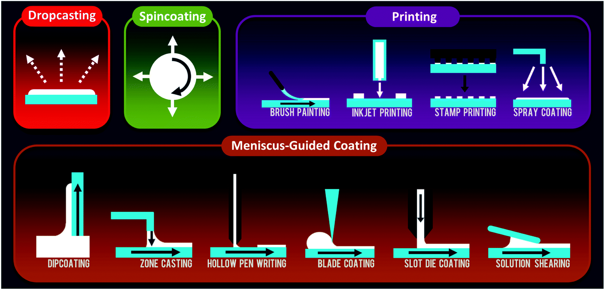 | ||
| Fig. 1 A schematic summary of the solution-based deposition techniques discussed. | ||
2.1 Dropcasting
A facile quasi-equilibrium process, dropcasting involves the casting of an OSC solution and the subsequent evaporation of the solvent to precipitate and deposit either individual crystals or a thin film. For OSCs with strong self-organizing behavior, single crystals can be obtained directly from dropcasting or from another recrystallization process. In the latter, a multistep process would consist of suspending the crystals in a nonsolvent and casting them again on a target substrate. One-step processes are also possible and would comprise the direct formation of crystals or thin films by one dropcasting event. A variety of modifications have been developed to enhance the quality of deposited crystals and thin films. For example, vibration-assisted crystallization – where the dropcast solution is exposed to unidirectional sound waves (∼100 Hz) during evaporation – was found to enhance crystal quality and device performance.1 In other cases, control of solvent evaporation was achieved by using mixed solvents, azeotropic mixtures,2 sealed chambers,3,4 saturated solvent environments,5 inert gas purging,6 and surface treatments.72.2 Spincoating
Spincoating is a commonly used solution method to form OSC thin films of effectively uniform thickness. The solution is dropped onto a substrate, and the substrate is accelerated to a high angular velocity to simultaneously spread the liquid and evaporate the solvent. The thickness of the wet film is inversely related to the spin speed and also depends on the solution concentration and viscosity. Spincoating is most often used to deposit the active layer, but there has also been research looking into the simultaneous, one-step deposition of both the semiconductor and the dielectric layer needed for many device applications.14 The vertical phase segregation and self-assembly of OSC/insulator pairs led to improvements in morphology and device performance in several instances.15,16Modifications of conventional spincoating have been used to fabricate high performance devices. Yuan et al. used an “off-center” method whereby the target substrate was placed 20 to 40 mm away from the central rotation axis.17 The centrifugal force in this modified technique – unlike the case of on-center spincoating, where solution is spread radially outward – facilitated unidirectional alignment of the resulting OSC thin film. Because of the kinetic nature of the process and the rapid solvent evaporation and film formation, a high performance, metastable molecular packing was achieved.
2.3 Meniscus-guided coating
Several solution coating techniques use the linear translation of either the substrate or the coating tool to induce aligned crystallite growth in the deposited thin films. These methods involve the evolution of a solution meniscus, which acts as an air–liquid interface for solvent evaporation. The solution concentrates with the removal of solvent, and once the point of supersaturation is reached, the solute precipitates and is deposited as thin film. In many of these techniques, alignment of the growing OSC thin film is achieved by virtue of the inherent directionality of the linear motion guiding the solution.Edge-casting is similar to other blading techniques in that a solution is simply coated over the substrate by the motion of solid surface above the droplet. Developed by Soeda et al., this method uses a flat, rectangular edge of a coating blade and can produce single-crystalline thin films by using slow solvent evaporation.28 A blade is moved at speeds on the order of tens of micrometers per second while sustaining a solution droplet in the gap between the rectangular blade and the substrate, which in ref. 28 was chosen to be 200 μm. The rectangular solution droplet was continuously fed with fresh solution so that the overall volume remained constant. High boiling point solvents (180 and 206 °C) were used with a moderate substrate temperature (80 °C) to deposit the films. To our knowledge, this technique has not been applied to OSC systems other than the ones from the first report, but the ability to form single crystals is quite attractive.
The combination of slot-die schemes with roll-to-roll processing has mostly been applied to solar cells30,31 and light-emitting diodes32 so far. The processing parameters that affect the previously discussed methods like zone casting and dipcoating are applicable here as well.
A modified solution shearing technique developed by Diao et al. recently demonstrated the deposition of organic semiconductor single crystals.39 Named “fluid-enhanced crystal engineering”, or FLUENCE, the method introduced two features to rationally control solute nucleation and crystal growth during deposition: (1) a shearing blade patterned with pillars to induce mixing within the sheared solution droplet and (2) a selectively wetting substrate with specially designed shapes. In the latter, the coffee-ring effect40 was used to induce nucleation, after which growing crystallites were filtered out so that only one could continue to grow. Mixing within the solution droplet served to reduce the mass transport limitations during crystallization.
2.4 Printing
The term “printing” is somewhat loosely defined, and while some may use the word to refer to a very specific type of deposition process, for the purposes of this review we categorize printing processes as those that are amenable to large-area deposition with spatial deposition control and that do not primarily rely on meniscus-driven coating.Several variations of the basic spray coating technique have been used for organic electronics applications. For example, multiple spray nozzles have been used in sequence to deposit different OSCs in a layer-by-layer fashion.58 Bulk heterojunction organic solar cells59 and LEDs60 have been fabricated using an evaporative spray technique, whereby very dilute solutions are first aerosolized into a heated chamber and then funnelled through a nozzle into a second chamber containing the target substrate.61 Ultrasonic spray nozzles have been used to atomize solutions to droplets on the scale of micrometers, as well as to prevent solution clogging within the nozzle.62–64 Lastly, electrospray deposition, where electricity is used to atomize the solution, was shown to effective for the selective deposition of organic materials on metal surfaces.65
3. Morphology control strategies for solution processing
As summarized in the previous section, recent years have witnessed rapid progress in the development of solution processing methods towards achieving the vision of low-cost, high-throughput, large-area fabrication of organic electronics. A key challenge in the area of solution-processed organic electronics lies in the precise control of thin film morphology during solution deposition. The critical role of thin film morphology in charge transport has been detailed in recent reviews.66–70There has been a long-held perception that most OSCs, when solution deposited, exhibit lower charge carrier mobilities than their vapor-deposited single crystal forms. In the last few years, such a perception has been frequently challenged by the rapid development in morphology control methods during solution processing, such as in the case of 6,13-bis(triisopropylsilylethynyl) pentacene (TIPS-pentacene)71–73 and dioctylbenzothienobenzothiophene (C8-BTBT).17,53 Thanks to the unique characteristics of solution processing methods, new avenues have been explored for controlling thin film morphology that are not easily implemented during vapor deposition, if at all possible. These new strategies include, but are not limited to, controlling the fluid flow,72,74 tuning the solvent composition by addition of an antisolvent or soluble additives,2,53,75 controlling evaporation rate using asymmetric patterns,7,53 contact line engineering,72 alignment control via meniscus guide,46,76etc. These recently developed morphology control strategies will be discussed in the following sections, which pertains to solution-processed organic field-effect transistors. The discussion will focus on three aspects: control of nucleation, crystal growth, and domain alignment, with special emphasis on methods that exploit the unique characteristics of solution processing.
3.1 Control of nucleation
Crystallization of OSCs is composed of two steps, nucleation and crystal growth. Nucleation involves overcoming of a free energy barrier and is intrinsically stochastic.77,78 Such properties often lead to random distribution of domain boundaries and domain sizes. This issue is not unique to solution processing and is also observed during vapor deposition. It is particularly important to control nucleation for the fabrication of single crystal arrays. Thus far, there have been relatively few methods reported on the control of OSC nucleation from solution, as summarized below.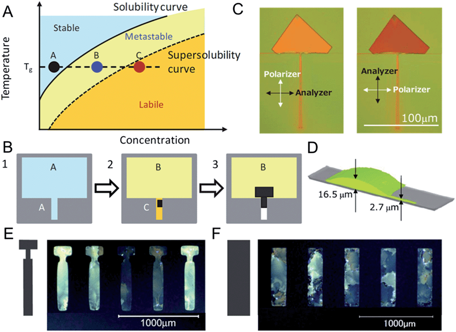 | ||
| Fig. 2 Nucleation controlled by solution volume asymmetry. Example 1 (A–D). (A) Solubility diagram corresponding to (B). (B) Schematic showing that nucleation occurs where solution volume is much lower. (C) Optical microscopy image of the resulting single crystals of C2Ph-PXX under cross-polarizers. (D) Calculation results of solution droplet shape. Example 2 (E–F). Comparison of ink-jet printed C8-BTBT thin film morphology with (E) and without (F) nucleation control region. Images are adapted with permission from ref. 53 (© 2011 Nature Publishing Group) and ref. 7 (© 2012 WILEY-VCH Verlag GmbH & Co. KGaA, Weinheim). | ||
 | ||
| Fig. 3 Nucleation controlled by tuning the contact line curvature. (A) Dependence of coffee ring thickness on contact line curvature. (B) Schematic of FLUENCE (fluid-enhanced crystal engineering) incorporated in solution shearing, wherein this nucleation control concept is implemented. (C) Design of wetting/dewetting zones for nucleation control (left) and the resulting morphology of FLUENCE-printed TIPS-pentacene thin films (right). The lower panel compares morphology obtained with and without nucleation control. The upper panel shows highly aligned single-crystalline domains obtained using FLUENCE, which extinguish cross-polarized light at once. All optical images were obtained under crossed polarized light. Images are adapted with permission from ref. 40 (© 1997 Nature Publishing Group) and ref. 72 (© 2013 Nature Publishing Group). | ||
Recently, two inert additives (DMDBS, BTA; Fig. 4a), originally designed for melt solidification of isotactic polypropylene (i-PP), were shown to effectively induce nucleation of a diverse set of OSCs by Stingelin, Chabinyc and coworkers.75 These two electrically insulating compounds initially dissolve at the molecular level in the molten polymer or solution, and, on cooling or solvent removal, form well-dispersed, nanoscopic surfaces for heterogeneous nucleation of the host material.
 | ||
| Fig. 4 Nucleation controlled using heterogeneous additives. (A) time-resolved microwave conductivity (TRMC) measurements of yield-mobility product of poly(3-dodecylthiophene) (P3DDT), neat (orange squares) and comprising DMDBS (black circles) or BTA (blue triangles). (B) Transmission optical micrographs of neat PCBM (99.5% electronic grade) drop cast at room temperature from chlorobenzene (left), with 0.1 wt% DMDBS (middle), and subsequently annealed at 180 °C. (C) Crossed-polarized optical micrographs (height: 660 μm and width: 820 μm) of an inkjet printed drop onto an OFET (Organic Field Effect Transistor) substrate with a dielectric treated with octadecyltrichlorosilane (OTS): ink comprising no nucleation agent (left); ink comprising a minute amount of DMDBS (right). Figures are adapted with permission from ref. 75 (© 2013 Nature Publishing Group). | ||
The authors found that the presence of the additive DMDBS in polymer P3DDT led to an increase of up to 50% in carrier yield compared with the neat polymer (Fig. 4a), which is attributed to the creation of a larger interfacial area between crystalline and amorphous domains through heterogeneous nucleation. A minute amount of DMDBS also reduced the domain sizes of annealed PCBM without adversely affecting the electron mobility. This effect was further explored as a patterning method by controlled deposition of the additive. With the nucleation agents, the authors also improved the device yield of bottom-contact TIPS-pentacene devices fabricated via ink-jet printing. The dielectric surface was functionalized with octadecyltrichlorosilane, a self-assembled monolayer shown extensively to improve charge transport in vapor deposited active layers.80 However, its low surface energy leads to dewetting of most organic solvents. Upon addition of DMDBS, the area coverage of TIPS-pentacene film greatly improved (Fig. 4c), whereas without the nucleation agent, the crystallization preferentially occurred on the Au electrodes. The yield of bottom contact transistor devices was therefore increased upon addition of the nucleating agent DMDBS. The hole mobility of the transistors was on the order of 10−2 cm2 V−1 s−1.
These examples show that enhanced nucleation using additives can greatly improve the device area coverage and can potentially enable device patterning by placing additives at pre-defined locations on the substrate. However, the addition of nucleation-inducing agents inevitably leads to reduction in domain sizes, which is often undesirable for transistor applications due to lowered charge carrier mobilities in cases where domain boundaries are rate-limiting – especially in the case of high-angle domain boundaries.81 Nonetheless, the reduction in domain size may prove beneficial to organic photovoltaic applications in some cases.
Other methods towards achieving nucleation control in vapor deposition or melt processing methods include the use of patterned rough surfaces,82,83 the use of chevron-shaped patterns for controlling silicon nucleation from its melt during laser annealing,84etc. Nonetheless, there is a very limited number of approaches developed for controlling nucleation of OSCs, largely due to the challenge of attempting to control an intrinsically stochastic process.
3.2 Control of crystal growth
Crystal growth control impacts the level of crystallinity/structural perfection, domain size distributions, substrate coverage, OSC-dielectric interface quality, etc., all of which are key to controlling the charge carrier mobility. In the following, we highlight three recently developed strategies for controlling crystal growth: by novel design of antisolvent crystallization, the new concept of flow-assisted crystallization, and solvent vapor annealing. These methods are designed to facilitate growth of large, highly crystalline domains by enhancing molecular mobility or eliminating mass transport limitations with the help of soft interfaces, fluid flow, or solvent vapor.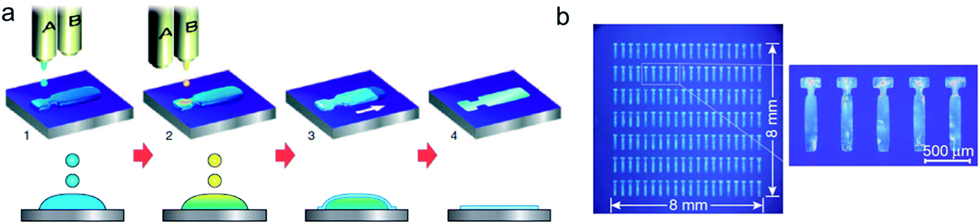 | ||
| Fig. 5 Crystal growth control via antisolvent crystallization. (a) Schematic of the process. Antisolvent ink (A) is first inkjet-printed (step 1), and then solution ink (B) is overprinted sequentially to form intermixed droplets confined to a predefined area (step 2). Semiconducting thin films grow at liquid–air interfaces of the droplet (step 3), before the solvent fully evaporates (step 4). (b) Micrographs of a 20 × 7 array of inkjet-printed C8-BTBT single-crystal thin films. Figures are adapted with permission from ref. 53 (© 2011 Nature Publishing Group). | ||
 | ||
| Fig. 6 Crystal growth controlled using micropillar arrays. (a) Schematic of solution shearing using a micropillar-patterned blade. For clarity, the micropillars are not drawn to scale. The arrow indicates the shearing direction. (b) A scanning electron micrograph of a micropillar-patterned blade. Inset, top view of the micropillars under an optical microscope. The pillars are 35 μm wide and 42 μm high. (c) Streamline representation of simulated fluid flow around the micropillars. The arrow indicates the flow direction. The streamlines are colour coded to indicate the scale of velocity (mm s−1), ranging from 0 (deep blue) to 1.3 mm s−1 (dark red). (d–f) Cross-polarized optical micrograph of a TIPS-pentacene film coated from its mesitylene solution with (d, right; f) and without micropillars (d, left; e), at a shearing speed of 0.6 mm s−1 g−1, Comparison of TIPS-pentacene coherence length with and without nucleation and crystal growth control along both parallel and perpendicular to shearing direction. (h and i) Comparison of 4T-TMS film morphology with and without using micropillar patterned blade. Figures are adapted with permission from ref. 72 (© 2013 Nature Publishing Group). | ||
In addition to directing the fluid flow using structured printing blades, another elegant approach has been developed by Cho and coworkers wherein Marangoni flow was induced using mixed solvents to overcome the coffee ring effect frequently observed during inkjet printing.74 Marangoni flow is a type of flow caused by a surface tension gradient, and the direction of the flow points towards higher surface tension regions. The convective flow that transports the solute to the contact line can be counterbalanced or enhanced, depending on the direction of the Marangoni flow. When adding a co-solvent of higher boiling point and lower surface tension, a Marangoni flow with a direction opposite that of the convective flow can be induced. On the other hand, the Marangoni flow can also enhance the convective flow if a low boiling point solvent with high surface tension is added as the minor component. Based on this strategy, the evaporation-induced flow in droplets can be controlled by varying the composition of the solvent mixture. The authors demonstrated this concept during ink-jet printing of TIPS-pentacene using chlorobenzene as a major solvent. When adding 25 vol% hexane (with lower boiling point and lower surface tension than the major solvent) as a minor solvent, the coffee-ring effect was found enhanced due to increased outward convective flow. When adding 25 vol% dodecane (with higher boiling point and lower surface tension than the major solvent), the coffee-ring effect was significantly reduced instead, thanks to the inward Marangoni flow (Fig. 7). Using this approach, both the film uniformity and the out-of-plane alignment were markedly improved, resulting in improved charge carrier mobility from 1.18 × 10⁻³ (hexane) to 0.12 cm2 V−1 s−1 (dodecane). Although currently only demonstrated with ink-jet printing, this approach may be educational to other printing methods for alleviating meniscus pinning, which causes uneven film morphology at times.
 | ||
| Fig. 7 Crystal growth controlled by inducing Maragoni flow. Optical microscope (OM) and polarized images of ink-jet-printed TIPS_PEN droplets with various solvent compositions: mixed-solvents containing chlorobenzene and 25 vol% (A) hexane and (B) dodecane (scale bar = 50 μm). Schematic diagrams of the evaporation-induced flow in a droplet during drying for various solvent compositions are shown under the corresponding images, where the arrows indicate the evaporation of solvent (blue), the outward convective flow (black), and the Marangoni flow (red). Images are adapted with permission from ref. 74 (© 2008 WILEY-VCH Verlag GmbH & Co. KGaA, Weinheim). | ||
Other methods for controlling crystal growth of solution-processed organic semiconductors include templated growth using thiol-functionalized electrodes to increase crystalline grain sizes,92 epitaxial growth of polymer films templated by solidified solvent crystals from undercooled solution,93–95 enhanced film morphology, crystallinity or interface quality using external fields (ultrasound,96 electric field,97 vibration98), etc.
3.3 Control of in-plane alignment
The impact of in-plane alignment of crystalline domains on charge carrier mobility has been fully demonstrated by studies on charge transport anisotropy. Within a single-crystalline domain, the mobility anisotropy is frequently on the order of 1–10.102–105 Across a polycrystalline film, the mobility anisotropy can range from a few times to several orders of magnitude depending on the nature of grain boundaries.81,86,93,106 Such sensitivity of charge transport to in-plane crystal orientation highlights the importance of controlling domain alignment. Over the past decade, many techniques have been developed to achieve in-plane alignment.68,70 This review will mainly focus on alignment methods newly developed within the past five years, which took advantage of the unique characteristics of solution processing, such as molecular assembly in a moving meniscus and under a flow field. | ||
| Fig. 8 Aligned crystal arrays using static meniscus guide. (A) An organic semiconductor droplet pinned by a silicon wafer. As the solvent evaporates slowly, the crystals of the organic semiconductors nucleate near the contact line of the droplet. Subsequently, the nuclei grow along the receding direction (toward the center) of the droplet. Optical microscopy images showing C60 crystals between source and drain electrodes. (B) Methods of fabricating the crystallized high-mobility C10-DNTT films on substrates using tilted stamps and resulting film morphology. Images are adapted with permission from ref. 46 (© 2012 American Chemical Society) and ref. 76 (©2011 WILEY-VCH Verlag GmbH & Co. KGaA, Weinheim). | ||
 | ||
| Fig. 9 Aligned crystal arrays using moving meniscus guide. (a and b) Schematic of zone casting and the resulting film morphology of dodecyl-substituted HBC derivative (HBC-C12).99 (c and d) Schematic of solution shearing and the resulting film morphology of TIPS-pentacene.33,71 (e) Schematic of hollow pen writing and the twin domains of TIPS-pentacene as a result.86 (f) Schematic of slot-die coating and the AFM image of the film with molecular structure superimposed.101 Images adapted with permission from ref. 99 (© 2005 WILEY-VCH Verlag GmbH & Co. KGaA, Weinheim), ref. 3 (© 2011 Nature Publishing Group), ref. 86 (© 2012 AIP Publishing LLC) and ref. 101 (© 2013 WILEY-VCH Verlag GmbH & Co. KGaA, Weinheim). | ||
Fig. 8 highlights two methods in which static meniscus guides were employed during solvent evaporation: drop-pinned crystallization76 and edge casting.46 In the first method, the OSC solution droplet is pinned using a small piece of silicon wafer. The authors also pointed out another important requirement for achieving alignment: high nuclei density (i.e., high solution concentration). Using this method, the authors have fabricated a variety of organic thin film transistors and inverters and demonstrated high charge carrier mobilities, enabled by improved alignment and crystal–dielectric interface.10,76 Particularly, aligned C60 single-crystal arrays prepared using this method yielded unprecedented electron mobilities as high as 11 cm2 V−1 s−1. In the method of edge casting, the meniscus is guided using inclined surfaces that cover the solution droplet during solvent evaporation (Fig. 8b). Using this method, the authors demonstrated aligned crystal arrays of 2,9-alkyl-dinaphtho[2,3-b:2′,3′-f]thieno[3,2-b]thiophene (C10-DNTT) with highest hole mobility exceeding 10 cm2 V−1 s−1. Both methods offer additional advantages besides alignment, such as patterned deposition over large area and the ability to handle low solubility organic semiconductors.
In recent years, a number of industry-compatible, large-area solution coating techniques (Fig. 9) have been developed for fabrication of aligned organic semiconductor thin films (mostly polycrystalline), such as zone casting,99 solution shearing,33,71–73 hollow-pen writing86,100 and slot-die coating,101 which we have surveyed in Section 1. A common feature of these methods is that the meniscus is guided by a moving surface, which can be provided by an ink-feeding head in some cases. One major advantage of moving meniscus guides as compared to static ones lies with the wide tunability of coating/printing speeds, which offers accessibility to a range of morphology features, from aligned polycrystalline thin films to spherulite formation.71,100,108 It also offers accessibility to nonequilibrium molecular packing, which was proved beneficial to enhancing charge carrier mobilities in the case of TIPS-pentacene.71,72 In fact, roll-to-roll printing methods frequently employ moving meniscus guides as well,25,31 and in those cases the fundamental molecular assembly processes are similar to those in the methods mentioned above.
Recently, Bao, Huang, and coworkers described the growth of highly aligned C8-BTBT from a blended solution of C8-BTBT and polystyrene using an off-center spin-coating method.17 In this method, the film alignment was achieved by guiding the meniscus motion using centrifugal force by placing the substrate in an off-center position (Fig. 10). The resulting C8-BTBT film was highly aligned and exhibited a metastable crystal packing. These morphological features combined with improved dielectric interface attained via vertical phase separation led to an ultrahigh hole mobility up to 43 cm2 V−1 s−1 (25 cm2 V−1 s−1 on average), which is the highest value reported to date for all organic molecules.
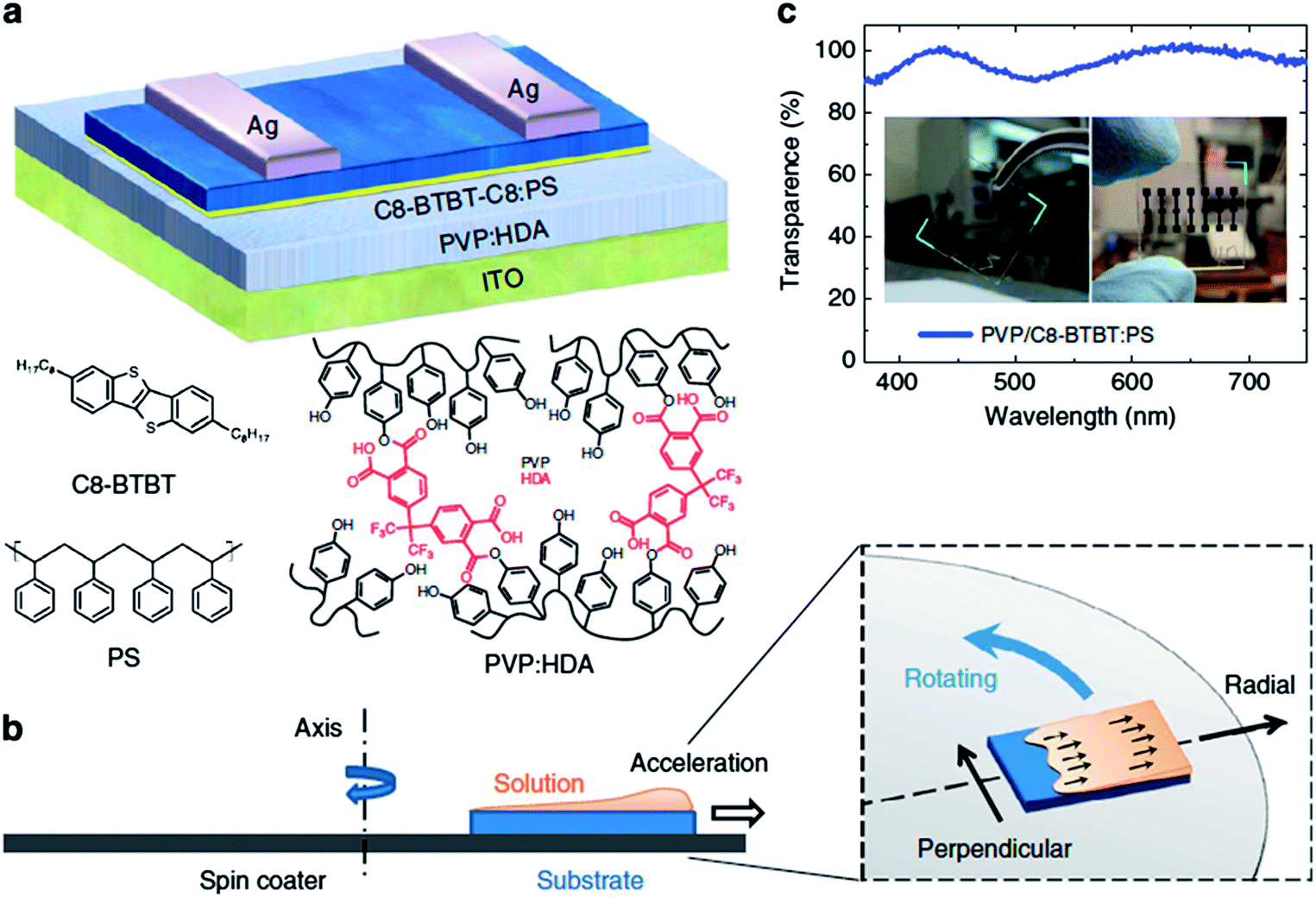 | ||
| Fig. 10 Highly aligned meta-stable C8-BTBT:PS film fabricated by off-center spin coating method. (a) Schematic device configuration of OTFT with C8-BTBT:PS blends as channel layer, PVP:HDA as dielectric layer and ITO as the gate electrode; the chemical structures of C8-BTBT, PS, PVP and HDA are shown. (b) Schematic illustration of the off-center spin coating process, in which the substrates are located away from the axis of the spin-coater. (c) Transmission spectrum of the PVP:HDA/C8-BTBT:PS film. Inset: photographs of C8-BTBT:PS film and corresponding OTFT device with a structure of glass/ITO/PVP:HDA/C8-BTBT:PS. Image adapted with permission from ref. 17 (© 2014 Nature Publishing Group). | ||
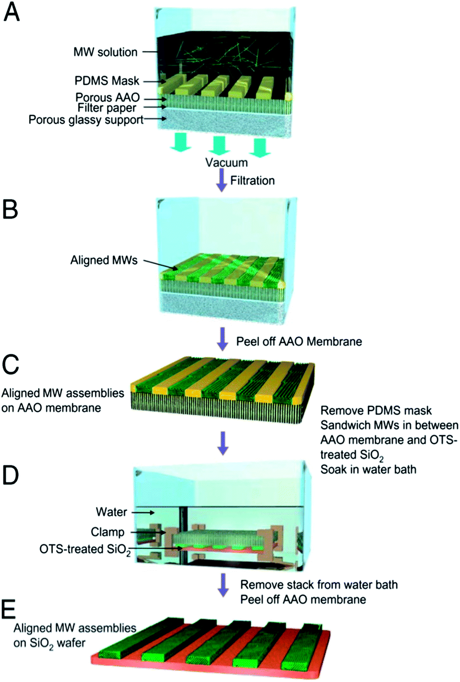 | ||
| Fig. 11 Schematic diagram for filtration and transfer (FAT) alignment of organic microwires. (A) FAT alignment apparatus loaded with the microwire dispersion. A PDMS mask with open-stripe patterns is placed on a porous AAO membrane. The microwire dispersion is filtered by applying vacuum. (B) Microwire assemblies reside exclusively inside the stripe patterns of the PDMS mask after filtration. The alignment of microwires along the stripe patterns is improved substantially as the pressure difference across the filter stack is increased. The density of the aligned microwires inside a single stripe pattern can be controlled by simply changing the concentration of the MW dispersion. (C) AAO membrane covered with patterned microwires inside the PDMS mask. (D) Illustration for the transfer of the aligned MW patterns from an AAO membrane to a desired wafer substrate in aqueous medium. Microwires selectively adhere to the OTS-treated SiO2 as water diffuses through the pores of the AAO membrane. (E) Aligned microwires were transferred onto the wafer. Images adapted with permission from ref. 115 (© 2009 National Academy of Sciences, USA). | ||
Besides in-plane alignment, out-of-plane alignment is desirable for both OTFT and OPV applications. The readers are referred to recent reviews covering this topic.70,120
4. Conclusions and outlook
The rapid advancement of thin film solution processing methods and morphology control strategies during recent years has brought us closer to the bright future promised by organic electronics applications. It is clear that choosing the appropriate processing method and deposition parameters is at least as important as the choice of organic semiconductor material. In order to fully exploit the potential of modern solution processing methods for organic semiconductors, a thorough understanding and control of the complex nucleation and crystal growth processes during thin film formation is indispensable. During solution processing, the crystal formation occurs in a multi-phase environment. Nucleation and crystal growth are critically influenced by the pairwise interactions between solute, solvent, and substrate, by the presence of phase boundaries, and by the multi-phase mass and heat transport processes. All these parameters jointly determine the morphology of organic semiconductor thin films, controlling which is key to achieving the desired electronic properties. Based on the understanding of these complexities during solution processing, strategies have been devised for tuning the morphological parameters relevant to device performance (grain sizes, grain boundaries, grain orientations, crystallinity, etc.) by controlling the fluid flow, tuning the solvent composition using antisolvent and additives, controlling evaporation rate using asymmetric patterns, or engineering the triple-phase contact line. Some of these strategies have been utilized for fabricating solution-processed single crystal arrays over a large area, which enabled record-setting charge carrier mobilities.17,39,53 Looking ahead, however, many challenges still remain, such as better control of defect densities, controlled formation and characterization of high quality OSC-dielectric interfaces, a quantitative understanding of the role of molecular packing on electronic properties, and morphological evolution in the context of high resolution printing where new phenomenon arise at sub-micron lengths scales, just to name a few. However, the numerous worldwide research efforts today (of which we could only capture a few in this review) and the large variety and steadily increasing quantity of reports describing new and innovative solution deposition methods for organic (plastic) electronics materials give confidence that most of these challenges will be successfully met in the near future.Acknowledgements
S.C.B.M., Z.B. and Y.D. acknowledge support by the Department of Energy, Bridging Research Interactions through collaborative Development Grants in Energy (BRIDGE) program under contract DE-FOA-0000654-1588. Z.B. and L.S. acknowledge support by the National Science Foundation (DMR-1303178), and L.S. gratefully thanks the Kodak Graduate Fellowship.Notes and references
- P. J. Diemer, C. R. Lyle, Y. Mei, C. Sutton, M. M. Payne, J. E. Anthony, V. Coropceanu, J.-L. Brédas and O. D. Jurchescu, Adv. Mater., 2013, 25, 6956–6962 CrossRef CAS PubMed.
- S. S. Lee, C. S. Kim, E. D. Gomez, B. Purushothaman, M. F. Toney, C. Wang, A. Hexemer, J. E. Anthony and Y.-L. Loo, Adv. Mater., 2009, 21, 3605–3609 CrossRef CAS.
- D. H. Kim, J. T. Han, Y. D. Park, Y. Jang, J. H. Cho, M. Hwang and K. Cho, Adv. Mater., 2006, 18, 719–723 CrossRef CAS.
- D. H. Kim, D. Y. Lee, H. S. Lee, W. H. Lee, Y. H. Kim, J. I. Han and K. Cho, Adv. Mater., 2007, 19, 678–682 CrossRef CAS.
- S. Wang, M. Kappl, I. Liebewirth, M. Müller, K. Kirchhoff, W. Pisula and K. Müllen, Adv. Mater., 2012, 24, 417–420 CrossRef CAS PubMed.
- J. Chen, C. K. Tee, M. Shtein, D. C. Martin and J. Anthony, Org. Electron., 2009, 10, 696–703 CrossRef CAS PubMed.
- O. Goto, S. Tomiya, Y. Murakami, A. Shinozaki, A. Toda, J. Kasahara and D. Hobara, Adv. Mater., 2012, 24, 1117–1122 CrossRef CAS PubMed.
- C. Zhang, X. Zhang, X. Zhang, X. Fan, J. Jie, J. C. Chang, C.-S. Lee, W. Zhang and S.-T. Lee, Adv. Mater., 2008, 20, 1716–1720 CrossRef CAS.
- H. Li, B. C. K. Tee, J. J. Cha, Y. Cui, J. W. Chung, S. Y. Lee and Z. Bao, J. Am. Chem. Soc., 2012, 134, 2760–2765 CrossRef CAS PubMed.
- H. Li, B. C. K. Tee, G. Giri, J. W. Chung, S. Y. Lee and Z. Bao, Adv. Mater., 2012, 24, 2588–2591 CrossRef CAS PubMed.
- U. Takafumi, H. Yuri, U. Mayumi, T. Kazuo and T. Jun, Appl. Phys. Express, 2009, 2, 111501 CrossRef.
- J. Soeda, Y. Hirose, M. Yamagishi, A. Nakao, T. Uemura, K. Nakayama, M. Uno, Y. Nakazawa, K. Takimiya and J. Takeya, Adv. Mater., 2011, 23, 3309–3314 CrossRef CAS PubMed.
- C. Mitsui, J. Soeda, K. Miwa, H. Tsuji, J. Takeya and E. Nakamura, J. Am. Chem. Soc., 2012, 134, 5448–5451 CrossRef CAS PubMed.
- L. L. Chua, P. K. H. Ho, H. Sirringhaus and R. H. Friend, Adv. Mater., 2004, 16, 1609–1615 CrossRef CAS.
- L. Qiu, J. A. Lim, X. Wang, W. H. Lee, M. Hwang and K. Cho, Adv. Mater., 2008, 20, 1141–1145 CrossRef CAS.
- C. Liu, Y. Li, M. V. Lee, A. Kumatani and K. Tsukagoshi, Phys. Chem. Chem. Phys., 2013, 15, 7917–7933 RSC.
- Y. Yuan, G. Giri, A. L. Ayzner, A. P. Zoombelt, S. C. B. Mannsfeld, J. Chen, D. Nordlund, M. F. Toney, J. Huang and Z. Bao, Nat. Commun., 2014, 5, 3005, DOI:10.1038/ncomms4005.
- R. Z. Rogowski, A. Dzwilewski, M. Kemerink and A. A. Darhuber, J. Phys. Chem. C, 2011, 115, 11758–11762 CAS.
- C.-Y. Liu and A. J. Bard, Chem. Mater., 2000, 12, 2353–2362 CrossRef CAS.
- A. Denneulin, A. Blayo, J. Bras and C. Neuman, Prog. Org. Coat., 2008, 63, 87–91 CrossRef CAS PubMed.
- C. E. Murphy, L. Yang, S. Ray, L. Yu, S. Knox and N. Stingelin, J. Appl. Phys., 2011, 110, 093523, DOI:10.1063/1.3660779.
- D. Khim, H. Han, K.-J. Baeg, J. Kim, S.-W. Kwak, D.-Y. Kim and Y.-Y. Noh, Adv. Mater., 2013, 25, 4302–4308 CrossRef CAS PubMed.
- Y.-H. Chang, S.-R. Tseng, C.-Y. Chen, H.-F. Meng, E.-C. Chen, S.-F. Horng and C.-S. Hsu, Org. Electron., 2009, 10, 741–746 CrossRef CAS PubMed.
- C.-Y. Chen, H.-W. Chang, Y.-F. Chang, B.-J. Chang, Y.-S. Lin, P.-S. Jian, H.-C. Yeh, H.-T. Chien, E.-C. Chen, Y.-C. Chao, H.-F. Meng, H.-W. Zan, H.-W. Lin, S.-F. Horng, Y.-J. Cheng, F.-W. Yen, I. F. Lin, H.-Y. Yang, K.-J. Huang and M.-R. Tseng, J. Appl. Phys., 2011, 110, 094501, DOI:10.1063/1.3636398.
- R. R. Søndergaard, M. Hösel and F. C. Krebs, J. Polym. Sci., Part B: Polym. Phys., 2013, 51, 16–34 CrossRef.
- S.-R. Tseng, H.-F. Meng, K.-C. Lee and S.-F. Horng, Appl. Phys. Lett., 2008, 93, 153308, DOI:10.1063/1.2999541.
- R. Bollström, A. Määttänen, D. Tobjörk, P. Ihalainen, N. Kaihovirta, R. Österbacka, J. Peltonen and M. Toivakka, Org. Electron., 2009, 10, 1020–1023 CrossRef PubMed.
- J. Soeda, T. Uemura, T. Okamoto, C. Mitsui, M. Yamagishi and J. Takeya, Appl. Phys. Express, 2013, 6, 076503 CrossRef.
- E. Cohen and E. J. Lightfoot, in Kirk-Othmer Encyclopedia of Chemical Technology, John Wiley & Sons, Inc., 2000 Search PubMed.
- F. C. Krebs, J. Fyenbo and M. Jorgensen, J. Mater. Chem., 2010, 20, 8994–9001 RSC.
- F. C. Krebs, Sol. Energy Mater. Sol. Cells, 2009, 93, 394–412 CrossRef CAS PubMed.
- A. Sandström, H. F. Dam, F. C. Krebs and L. Edman, Nat. Commun., 2012, 3, 1002 CrossRef PubMed.
- H. A. Becerril, M. E. Roberts, Z. Liu, J. Locklin and Z. Bao, Adv. Mater., 2008, 20, 2588–2594 CrossRef CAS.
- Z. Liu, H. A. Becerril, M. E. Roberts, Y. Nishi and Z. Bao, IEEE Trans. Electron Devices, 2009, 56, 176–185 CrossRef CAS.
- G. Giri, E. Verploegen, S. C. B. Mannsfeld, S. Atahan-Evrenk, D. H. Kim, S. Y. Lee, H. A. Becerril, A. Aspuru-Guzik, M. F. Toney and Z. Bao, Nature, 2011, 480, 504–508 CrossRef CAS PubMed.
- V. Coropceanu, J. Cornil, D. A. da Silva Filho, Y. Olivier, R. Silbey and J.-L. Brédas, Chem. Rev., 2007, 107, 926–952 CrossRef CAS PubMed.
- R. S. Sánchez-Carrera, S. Atahan, J. Schrier and A. n. Aspuru-Guzik, J. Phys. Chem. C, 2010, 114, 2334–2340 Search PubMed.
- J. Cornil, D. Beljonne, J. P. Calbert and J. L. Brédas, Adv. Mater., 2001, 13, 1053–1067 CrossRef CAS.
- Y. Diao, B. C. K. Tee, G. Giri, J. Xu, D. H. Kim, H. A. Becerril, R. M. Stoltenberg, T. H. Lee, G. Xue, S. C. B. Mannsfeld and Z. Bao, Nat. Mater., 2013, 12, 665–671 CrossRef CAS PubMed.
- R. D. Deegan, O. Bakajin, T. F. Dupont, G. Huber, S. R. Nagel and T. A. Witten, Nature, 1997, 389, 827–829 CrossRef CAS PubMed.
- S. S. Kim, S. I. Na, J. Jo, G. Tae and D. Y. Kim, Adv. Mater., 2007, 19, 4410–4415 CrossRef CAS.
- S.-S. Kim, S.-I. Na, S.-J. Kang and D.-Y. Kim, Sol. Energy Mater. Sol. Cells, 2010, 94, 171–175 CrossRef CAS PubMed.
- M. Ikawa, T. Yamada, H. Matsui, H. Minemawari, J. y. Tsutsumi, Y. Horii, M. Chikamatsu, R. Azumi, R. Kumai and T. Hasegawa, Nat. Commun., 2012, 3, 1176 CrossRef PubMed.
- H. B. Akkerman, A. C. Chang, E. Verploegen, C. J. Bettinger, M. F. Toney and Z. Bao, Org. Electron., 2012, 13, 235–243 CrossRef CAS PubMed.
- M. Cavallini, P. Stoliar, J.-F. Moulin, M. Surin, P. Leclère, R. Lazzaroni, D. W. Breiby, J. W. Andreasen, M. M. Nielsen, P. Sonar, A. C. Grimsdale, K. Müllen and F. Biscarini, Nano Lett., 2005, 5, 2422–2425 CrossRef CAS PubMed.
- K. Nakayama, Y. Hirose, J. Soeda, M. Yoshizumi, T. Uemura, M. Uno, W. Li, M. J. Kang, M. Yamagishi, Y. Okada, E. Miyazaki, Y. Nakazawa, A. Nakao, K. Takimiya and J. Takeya, Adv. Mater., 2011, 23, 1626–1629 CrossRef CAS PubMed.
- P. S. Jo, A. Vailionis, Y. M. Park and A. Salleo, Adv. Mater., 2012, 24, 3269–3274 CrossRef CAS PubMed.
- Z. Zheng, K.-H. Yim, M. S. M. Saifullah, M. E. Welland, R. H. Friend, J.-S. Kim and W. T. S. Huck, Nano Lett., 2007, 7, 987–992 CrossRef CAS PubMed.
- M. Singh, H. M. Haverinen, P. Dhagat and G. E. Jabbour, Adv. Mater., 2010, 22, 673–685 CrossRef CAS PubMed.
- B. Derby, Annu. Rev. Mater. Res., 2010, 40, 395–414 CrossRef CAS.
- B.-J. de Gans and U. S. Schubert, Langmuir, 2004, 20, 7789–7793 CrossRef CAS PubMed.
- H. Sirringhaus, T. Kawase, R. H. Friend, T. Shimoda, M. Inbasekaran, W. Wu and E. P. Woo, Science, 2000, 290, 2123–2126 CrossRef CAS.
- H. Minemawari, T. Yamada, H. Matsui, J. y. Tsutsumi, S. Haas, R. Chiba, R. Kumai and T. Hasegawa, Nature, 2011, 475, 364–367 CrossRef CAS PubMed.
- A. C. Arias, S. E. Ready, R. Lujan, W. S. Wong, K. E. Paul, A. Salleo, M. L. Chabinyc, R. Apte, R. A. Street, Y. Wu, P. Liu and B. Ong, Appl. Phys. Lett., 2004, 85, 3304–3306 CrossRef CAS PubMed.
- A. Abdellah, B. Fabel, P. Lugli and G. Scarpa, Org. Electron., 2010, 11, 1031–1038 CrossRef CAS PubMed.
- D. Vak, S.-S. Kim, J. Jo, S.-H. Oh, S.-I. Na, J. Kim and D.-Y. Kim, Applied Physics Letters, 2007, 91, 081102, DOI:10.1063/1.2772766.
- S. F. Tedde, J. Kern, T. Sterzl, J. Fürst, P. Lugli and O. Hayden, Nano Lett., 2009, 9, 980–983 CrossRef CAS PubMed.
- L.-M. Chen, Z. Hong, W. L. Kwan, C.-H. Lu, Y.-F. Lai, B. Lei, C.-P. Liu and Y. Yang, ACS Nano, 2010, 4, 4744–4752 CrossRef CAS PubMed.
- T. Ishikawa, M. Nakamura, K. Fujita and T. Tsutsui, Appl. Phys. Lett., 2004, 84, 2424–2426 CrossRef CAS PubMed.
- Y. Aoki, M. Shakutsui and K. Fujita, Thin Solid Films, 2009, 518, 493–496 CrossRef CAS PubMed.
- K. Fujita, T. Ishikawa and T. Tsutsui, Jpn. J. Appl. Phys., Part 1, 2002, 41, L70 CrossRef CAS.
- M. Shao, S. Das, K. Xiao, J. Chen, J. K. Keum, I. N. Ivanov, G. Gu, W. Durant, D. Li and D. B. Geohegan, J. Mater. Chem. C, 2013, 1, 4384–4390 RSC.
- R. C. Tenent, T. M. Barnes, J. D. Bergeson, A. J. Ferguson, B. To, L. M. Gedvilas, M. J. Heben and J. L. Blackburn, Adv. Mater., 2009, 21, 3210–3216 CrossRef CAS.
- K. X. Steirer, M. O. Reese, B. L. Rupert, N. Kopidakis, D. C. Olson, R. T. Collins and D. S. Ginley, Sol. Energy Mater. Sol. Cells, 2009, 93, 447–453 CrossRef CAS PubMed.
- J. Ju, Y. Yamagata and T. Higuchi, Adv. Mater., 2009, 21, 4343–4347 CrossRef CAS.
- J. A. Lim, H. S. Lee, W. H. Lee and K. Cho, Adv. Funct. Mater., 2009, 19, 1515–1525 CrossRef CAS.
- A. A. Virkar, S. Mannsfeld, Z. Bao and N. Stingelin, Adv. Mater., 2010, 22, 3857–3875 CrossRef CAS PubMed.
- S. Liu, W. M. Wang, A. L. Briseno, S. C. E. Mannsfeld and Z. Bao, Adv. Mater., 2009, 21, 1217–1232 CrossRef CAS.
- S. S. Lee and Y.-L. Loo, Annu. Rev. Chem. Biomol. Eng., 2010, 1, 59–78 CrossRef CAS PubMed.
- A. M. Hiszpanski and Y.-L. Loo, Energy Environ. Sci., 2014, 7, 592–608 CAS.
- G. Giri, E. Verploegen, S. C. B. Mannsfeld, S. Atahan-Evrenk, D. H. Kim, S. Y. Lee, H. A. Becerril, A. Aspuru-Guzik, M. F. Toney and Z. A. Bao, Nature, 2011, 480, 504–U124 CrossRef CAS PubMed.
- Y. Diao, B. C. K. Tee, G. Giri, J. Xu, D. H. Kim, H. A. Becerril, R. M. Stoltenberg, T. H. Lee, G. Xue, S. C. B. Mannsfeld and Z. N. Bao, Nat. Mater., 2013, 12, 665–671 CrossRef CAS PubMed.
- B. D. Naab, S. Himmelberger, Y. Diao, K. Vandewal, P. Wei, B. Lussem, A. Salleo and Z. Bao, Adv. Mater., 2013, 25, 4663–4667 CrossRef CAS PubMed.
- J. A. Lim, W. H. Lee, H. S. Lee, J. H. Lee, Y. D. Park and K. Cho, Adv. Funct. Mater., 2008, 18, 229–234 CrossRef CAS.
- N. D. Treat, J. A. N. Malik, O. Reid, L. Yu, C. G. Shuttle, G. Rumbles, C. J. Hawker, M. L. Chabinyc, P. Smith and N. Stingelin, Nat. Mater., 2013, 12, 628–633 CrossRef CAS PubMed.
- H. Li, B. C. K. Tee, J. J. Cha, Y. Cui, J. W. Chung, S. Y. Lee and Z. Bao, J. Am. Chem. Soc., 2012, 134, 2760–2765 CrossRef CAS PubMed.
- Y. Diao, A. S. Myerson, T. A. Hatton and B. L. Trout, Langmuir, 2011, 27, 5324–5334 CrossRef CAS PubMed.
- Y. Diao, M. E. Helgeson, Z. A. Siam, P. S. Doyle, A. S. Myerson, T. A. Hatton and B. L. Trout, Cryst. Growth Des., 2011, 12, 508–517 Search PubMed.
- S. S. Lee, S. Muralidharan, A. R. Woll, M. A. Loth, Z. Li, J. E. Anthony, M. Haataja and Y.-L. Loo, Chem. Mater., 2012, 24, 2920–2928 CrossRef CAS.
- Y. Ito, A. A. Virkar, S. Mannsfeld, J. H. Oh, M. Toney, J. Locklin and Z. Bao, J. Am. Chem. Soc., 2009, 131, 9396–9404 CrossRef CAS PubMed.
- J. Rivnay, L. H. Jimison, J. E. Northrup, M. F. Toney, R. Noriega, S. Lu, T. J. Marks, A. Facchetti and A. Salleo, Nat. Mater., 2009, 8, 952–958 CrossRef CAS PubMed.
- A. L. Briseno, S. C. B. Mannsfeld, M. M. Ling, S. Liu, R. J. Tseng, C. Reese, M. E. Roberts, Y. Yang, F. Wudl and Z. Bao, Nature, 2006, 444, 913–917 CrossRef CAS PubMed.
- S. Liu, A. L. Briseno, S. C. B. Mannsfeld, W. You, J. Locklin, H. W. Lee, Y. Xia and Z. Bao, Adv. Funct. Mater., 2007, 17, 2891–2896 CrossRef CAS.
- A. Hara and N. Sasaki, J. Appl. Phys., 2000, 88, 3349–3353 CrossRef CAS PubMed.
- L. Li, P. Gao, K. C. Schuermann, S. Ostendorp, W. Wang, C. Du, Y. Lei, H. Fuchs, L. De Cola, K. Muellen and L. Chi, J. Am. Chem. Soc., 2010, 132, 8807–8809 CrossRef CAS PubMed.
- S. Wo, R. L. Headrick and J. E. Anthony, J. Appl. Phys., 2012, 111, 073716, DOI:10.1063/1.3698203.
- D. J. Mascaro, M. E. Thompson, H. I. Smith and V. Bulović, Org. Electron., 2005, 6, 211–220 CrossRef CAS PubMed.
- K. C. Dickey, J. E. Anthony and Y. L. Loo, Adv. Mater., 2006, 18, 1721–1726 CrossRef CAS.
- S. S. Lee, S. B. Tang, D.-M. Smilgies, A. R. Woll, M. A. Loth, J. M. Mativetsky, J. E. Anthony and Y.-L. Loo, Adv. Mater., 2012, 24, 2692–2698 CrossRef CAS PubMed.
- C. Liu, T. Minari, X. Lu, A. Kumatani, K. Takimiya and K. Tsukagoshi, Adv. Mater., 2011, 23, 523–526 CrossRef CAS PubMed.
- H. Ullah Khan, R. Li, Y. Ren, L. Chen, M. M. Payne, U. S. Bhansali, D.-M. Smilgies, J. E. Anthony and A. Amassian, ACS Appl. Mater. Interfaces, 2013, 5, 2325–2330 CAS.
- D. J. Gundlach, J. E. Royer, S. K. Park, S. Subramanian, O. D. Jurchescu, B. H. Hamadani, A. J. Moad, R. J. Kline, L. C. Teague, O. Kirillov, C. A. Richter, J. G. Kushmerick, L. J. Richter, S. R. Parkin, T. N. Jackson and J. E. Anthony, Nat. Mater., 2008, 7, 216–221 CrossRef CAS PubMed.
- L. H. Jimison, M. F. Toney, I. McCulloch, M. Heeney and A. Salleo, Adv. Mater., 2009, 21, 1568–1572 CrossRef CAS.
- M. Brinkmann and J. C. Wittmann, Adv. Mater., 2006, 18, 860–863 CrossRef CAS.
- C. De Rosa, C. Park, E. L. Thomas and B. Lotz, Nature, 2000, 405, 433–437 CrossRef CAS PubMed.
- A. R. Aiyar, J.-I. Hong, R. Nambiar, D. M. Collard and E. Reichmanis, Adv. Funct. Mater., 2011, 21, 2652–2659 CrossRef CAS.
- T. Komino, H. Kuwabara, M. Ikeda, M. Yahiro, K. Takimiya and C. Adachi, Langmuir, 2013, 29, 9592–9597 CrossRef CAS PubMed.
- P. J. Diemer, C. R. Lyle, Y. Mei, C. Sutton, M. M. Payne, J. E. Anthony, V. Coropceanu, J.-L. Brédas and O. D. Jurchescu, Adv. Mater., 2013, 25, 6956–6962 CrossRef CAS PubMed.
- W. Pisula, A. Menon, M. Stepputat, I. Lieberwirth, U. Kolb, A. Tracz, H. Sirringhaus, T. Pakula and K. Mullen, Adv. Mater., 2005, 17, 684–689 CrossRef CAS.
- R. L. Headrick, S. Wo, F. Sansoz and J. E. Anthony, Appl. Phys. Lett., 2008, 92, 063302, DOI:10.1063/1.2839394.
- J. Chang, C. Chi, J. Zhang and J. Wu, Adv. Mater., 2013, 25, 6442–6447 CrossRef CAS PubMed.
- V. Podzorov, E. Menard, A. Borissov, V. Kiryukhin, J. A. Rogers and M. E. Gershenson, Phys. Rev. Lett., 2004, 93, 086602, DOI:10.1103/PhysRevLett.93.086602.
- S. C. B. Mannsfeld, J. Locklin, C. Reese, M. E. Roberts, A. J. Lovinger and Z. Bao, Adv. Funct. Mater., 2007, 17, 1617–1622 CrossRef CAS.
- J. L. Bredas, J. P. Calbert, D. A. da Silva and J. Cornil, Proc. Natl. Acad. Sci. U. S. A., 2002, 99, 5804–5809 CrossRef CAS PubMed.
- V. Coropceanu, J. Cornil, D. A. da Silva, Y. Olivier, R. Silbey and J. L. Bredas, Chem. Rev., 2007, 107, 926–952 CrossRef CAS PubMed.
- C. W. Sele, B. K. C. Kjellander, B. Niesen, M. J. Thornton, J. B. P. H. van der Putten, K. Myny, H. J. Wondergem, A. Moser, R. Resel, A. J. J. M. van Breemen, N. van Aerle, P. Heremans, J. E. Anthony and G. H. Gelinck, Adv. Mater., 2009, 21, 4926–4931 CrossRef CAS.
- M. Le Berre, Y. Chen and D. Baigl, Langmuir, 2009, 25, 2554–2557 CrossRef CAS PubMed.
- R. Z. Rogowski and A. A. Darhuber, Langmuir, 2010, 26, 11485–11493 CrossRef CAS PubMed.
- T. Uemura, Y. Hirose, M. Uno, K. Takimiya and J. Takeya, Appl. Phys. Express, 2009, 2, 111501, DOI:10.1143/apex.2.111501.
- W. H. Lee, D. H. Kim, Y. Jang, J. H. Cho, M. Hwang, Y. D. Park, Y. H. Kim, J. I. Han and K. Cho, Appl. Phys. Lett., 2007, 90, 132106, DOI:10.1063/1.2717087.
- T. Lei and J. Pei, J. Mater. Chem., 2012, 22, 785–798 RSC.
- N. Liu, Y. Zhou, N. Ai, C. Luo, J. Peng, J. Wang, J. Pei and Y. Cao, Langmuir, 2011, 27, 14710–14715 CrossRef CAS PubMed.
- W. Jiang, Y. Zhou, H. Geng, S. Jiang, S. Yan, W. Hu, Z. Wang, Z. Shuai and J. Pei, J. Am. Chem. Soc., 2010, 133, 1–3 CrossRef PubMed.
- D. H. Kim, D. Y. Lee, H. S. Lee, W. H. Lee, Y. H. Kim, J. I. Han and K. Cho, Adv. Mater., 2007, 19, 678–682 CrossRef CAS.
- J. H. Oh, H. W. Lee, S. Mannsfeld, R. M. Stoltenberg, E. Jung, Y. W. Jin, J. M. Kim, J.-B. Yoo and Z. Bao, Proc. Natl. Acad. Sci. U. S. A., 2009, 106, 6065–6070 CrossRef CAS PubMed.
- G. H. Yu, A. Y. Cao and C. M. Lieber, Nat. Nanotechnol., 2007, 2, 372–377 CrossRef CAS PubMed.
- Y. Z. Long, M. Yu, B. Sun, C. Z. Gu and Z. Y. Fan, Chem. Soc. Rev., 2012, 41, 4560–4580 RSC.
- C. M. Schroeder, E. S. G. Shaqfeh and S. Chu, Macromolecules, 2004, 37, 9242–9256 CrossRef CAS.
- A. B. Marciel, M. Tanyeri, B. D. Wall, J. D. Tovar, C. M. Schroeder and W. L. Wilson, Adv. Mater., 2013, 25, 6398–6404 CrossRef CAS PubMed.
- W. H. Lee, J. H. Cho and K. Cho, J. Mater. Chem., 2010, 20, 2549–2561 RSC.
| This journal is © The Royal Society of Chemistry 2014 |