 Open Access Article
 This Open Access Article is licensed under a
 Creative Commons Attribution 3.0 Unported Licence
Al-doped ZnO inverse opal networks as efficient electron collectors in BiVO4 photoanodes for solar water oxidation†
Liwu
Zhang
a,
Erwin
Reisner
*b and
Jeremy J.
Baumberg
*a
aCavendish Laboratory, Department of Physics, University of Cambridge, Cambridge, CB3 0HE, UK. E-mail: jjb12@cam.ac.uk
bChristian Doppler Laboratory for Sustainable SynGas Chemsitry, Department of Chemistry, University of Cambridge, Cambridge, CB2 1EW, UK. E-mail: reisner@ch.cam.ac.uk
First published on 24th February 2014
Abstract
The short diffusion length of photogenerated charge carriers limits the performance of photoelectrodes for solar water splitting. To reduce the distance between where the charges are generated and the location they are scavenged, a conductive Al-doped ZnO inverse opal network is introduced into a BiVO4 photoanode. The conductive inverse opal network serves as an electron collector for the BiVO4 film, which suffers from poor electron transport. The combined heterostructure provides a photocurrent of 1.5 mA cm−2 at 1.23 V vs. RHE, which is threefold higher than a BiVO4 photoanode without any conducting inverse opal network. The significantly enhanced photocurrent produced without intentional doping or oxygen-evolving catalysts, indicates the importance of charge transport and collection in photoelectrodes. Our design has the potential to be applied to other photoelectrochemical systems to improve charge collection and solar energy conversion efficiency.
Broader contextPhotoelectrochemical water splitting is an attractive approach to meet the urgent goal of efficiently and inexpensively converting solar energy into a storable and transportable fuel. A lack of efficient and inexpensive photoelectrodes inhibits the practical application of this technology. The short diffusion length of photogenerated charge carriers limits the performance of photoelectrodes for solar water splitting. We introduce a conductive Al-doped ZnO inverse opal network into a BiVO4 photoanode, which has poor electron transport performance. The conductive inverse opal network serves as an electron collector for the BiVO4 film and this approach enhances the photocurrent by three times compared to a planar BiVO4 film. The enhanced performance is attributed to the improved charge transport and collection in the photoelectrode with the conductive inverse opal network. This design has the potential to improve the performance of other solar water splitting systems. |
Artificial photosynthesis is an attractive approach to meet the urgent goal of efficiently and inexpensively converting solar energy into a storable and transportable form.1,2 Photoelectrochemical water splitting is a promising and environmentally friendly route for the conversion of solar energy into hydrogen. The development of solar water splitting devices provides also an important first step towards the goal of developing artificial leaves capable of converting CO2 directly into liquid fuels.3 Currently, a lack of efficient, inexpensive and scalable photoelectrodes limits the practical application and development of this technology.
Many metal oxides are inexpensive, robust and easily fabricated and they are therefore frequently studied photoelectrode materials.4–9 Post-transition metal cations having electronic configurations with ns2 [e.g., PbO (2.1 eV) and Bi2O3 (2.5 eV)] or transition metal cations with dn [e.g., Fe2O3 (Eg = 2.0 eV) and Cu2O (2.0 eV)] can produce binary metal oxides with narrow band gap energies. However, the former metal oxides show unfavourable indirect band gap transitions resulting from the coupling between the filled cation s and anion p states, whereas the latter oxides suffer from high resistivities due to the small polaron-dominated conductivity. To overcome the intrinsic limitations of binary metal oxides, multiple cations can be combined to form multinary oxides.10,11 Among these multinary metal oxides, bismuth vanadate (BiVO4) has been identified as one of the most promising n-type semiconductors as photoanodes for water splitting. BiVO4, with a band gap of 2.4 eV, was first reported by Kudo and coworkers as a photocatalyst for water oxidation.12 Since then BiVO4 has been studied as a visible-light-driven photocatalyst for the degradation of organic compounds and water oxidation.13–16 Recently, extensive attention has focused on BiVO4 as a photoanode for photoelectrochemical water splitting.17–21 To improve the charge transport properties and reduce the surface recombination of the photogenerated carriers in BiVO4, great efforts have been made by doping, introducing water oxidation cocatalysts, constructing nanostructures, etc.18,20,22–26 It has been demonstrated by van de Krol and coworkers that, contrary to α-Fe2O3 which has a short hole diffusion length, BiVO4 suffers from poor electron transfer and collection in the photoelectrode.27 Poor electron transport results in high bulk recombination of photogenerated charge carriers and thus a low solar-to-H2 conversion efficiency.
To address this issue, we introduce here a conductive network into the BiVO4 film to improve the photogenerated electron collection. An Al-doped ZnO inverse opal (io-AZO) structure is for the first time employed to serve as a charge-transport pathway in the photoelectrode. The inverse opal conductive network is prepared via an opal template by evaporation-induced self-assembly of polystyrene spheres (PS). The crystallized io-AZO structure is obtained after infiltration of the PS network with an aqueous Zn(acetate)2 and Al(NO3)3 precursor solution and removing the PS opal template by annealing. The pores in the AZO inverse opal structure are then filled with BiVO4 precursor solution and annealed to achieve a BiVO4/io-AZO heterostructured photoanode. The procedure for this heterostructure fabrication is illustrated in Scheme 1.
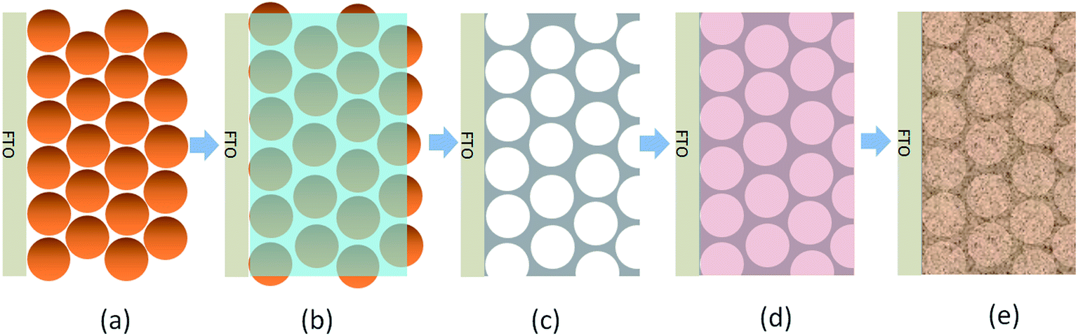 | ||
| Scheme 1 Synthesis of the BiVO4/io-AZO heterostructure photoanode. (a) Opal template formed on FTO by evaporation-induced self-assembly of PS beads. (b) Infiltration of AZO precursor into the void of the opal template. (c) Removal of template and crystallizing AZO network by annealing. (d) Filling pores of io-AZO with BiVO4 precursor. (e) Formation of BiVO4/io-AZO heterostructure by annealing. | ||
The morphology and crystal structure of the io-AZO charge-collecting support structure and BiVO4/io-AZO heterostructures are investigated by scanning electron microscopy (SEM) and X-ray diffraction (XRD). Fig. 1a displays the three-dimensionally-ordered macroporous structure of the io-AZO film. The hexagonal close-packed structure shows a pore size of approximately 300 nm with each pore connected to an adjacent pore by a small hole of about 80 nm in diameter. This continuous structure allows infiltration of the BiVO4 precursor solution into the entire film and formation of a uniform heterostructure. In this hybrid architecture, the inverse opal structure serves as a charge-collecting support structure. The SEM image of the assembled BiVO4/io-AZO heterostructure is shown in Fig. 1b. BiVO4 is found both inside and on the surface of the io-AZO film. The framework of the io-AZO can still be clearly observed underneath the layer of BiVO4 on the top surface. Compared with the io-AZO without BiVO4 (Fig. 1a), it is found that upon deposition of BiVO4 onto the walls of io-AZO, the structure of io-AZO is well maintained. Fig. 1c shows the X-ray diffraction (XRD) patterns of a BiVO4/io-AZO electrode. The peaks are assigned to the scheelite-monoclinic phase of BiVO4 (JCPDS no. 14-0688) and the zincite structure of ZnO (JCPDS no. 89-1397), indicating the formation of the desired BiVO4/io-AZO heterostructure in the photoelectrode. Zn-doping of BiVO4 could have occurred during the annealing process and Zn-doping was previously shown to give a negative effect on the photocatalytic performance of BiVO4.24 However, significant Zn-doping of BiVO4 is not observed in the BiVO4/io-AZO heterostructure with no significant peak shifts in the XRD spectra in BiVO4/io-AZO. Fig. 1d illustrates the advantage of this design for solar water oxidation. In a planar BiVO4 film, the electrons excited in the bulk film (where the thickness is longer than the electron diffusion length) cannot be collected by FTO due to the poor electron transport in BiVO4. However, in the BiVO4/io-AZO heterostructure design, the distance needed for the electron transport is much shorter. The conductive io-AZO network can thus effectively collect the photogenerated electrons.
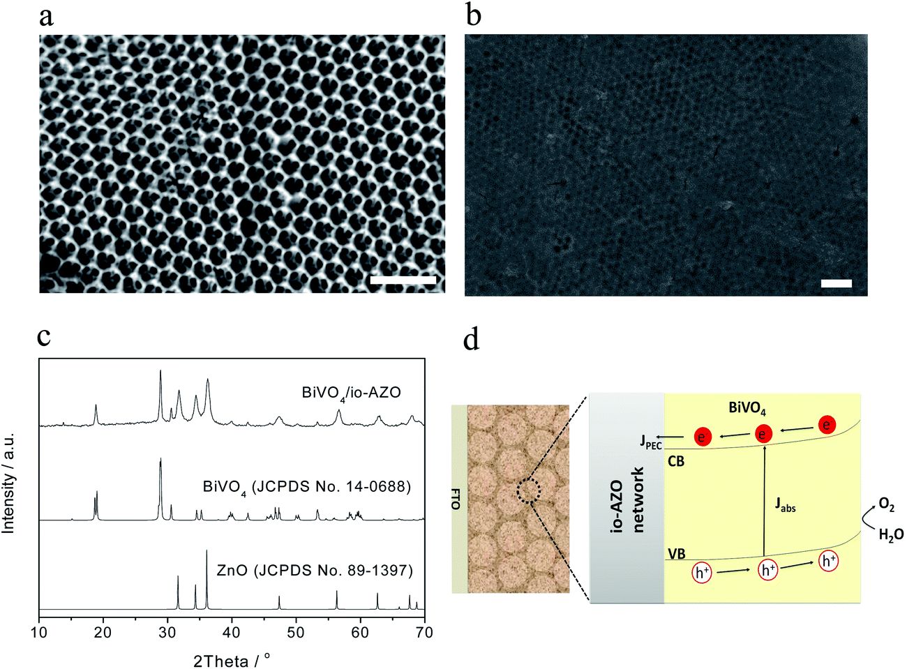 | ||
| Fig. 1 (a) SEM image of the io-AZO electrode. (b) SEM image of the BiVO4/io-AZO heterostructure. (c) XRD pattern of the BiVO4/io-AZO heterostructure. (d) Schematic illustration of the BiVO4/io-AZO heterostructure, where the conductive io-AZO network can readily collect the photogenerated electrons. The scale bars in 1(a) and 1(b) are 1 μm. | ||
The photoelectrochemical response of the planar BiVO4 and BiVO4/io-AZO heterostructure electrodes were studied both in the dark and under AM 1.5G illumination (100 mW cm−2). A conventional three electrode configuration was used with BiVO4 on FTO as working electrode, a Pt wire as the counter electrode, and a Ag/AgCl reference electrode. All the potentials are reported against the reversible hydrogen electrode (RHE). The electrolyte was aqueous phosphate buffer at pH 7 without any additive. Fig. 2a shows the linear voltammetry sweeps (scan rate: 10 mV s−1) on the planar BiVO4 and BiVO4/io-AZO anodes under chopped illumination from the backside of the electrodes. The anodic photocurrent was observed once the open-circuit potential of 0.5 V was exceeded and the photocurrent increased steadily with the applied positive potential, whereas the currents are negligible in the dark. It is evident that an enhanced photocurrent is obtained essentially over the entire potential range for the BiVO4/io-AZO heterostructure. In particular, for both electrodes, the photocurrent increased more or less linearly as the potential rises from 0.8 to 1.2 V. It is notable that there is a threefold difference in the slope (photocurrent vs. potential) between the two films. The slope corresponds to the inverse resistance of contact between the working electrode material and the electrolyte,28 implying the BiVO4/io-AZO heterostructure has lower resistance, and as a consequence, the photocurrent increased rapidly with applied potential.
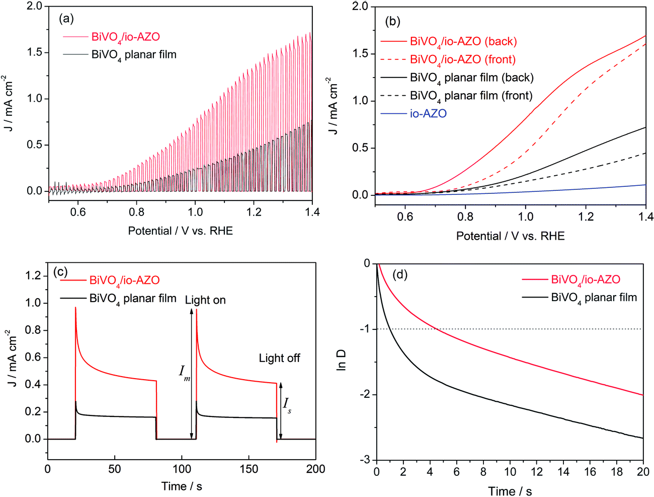 | ||
| Fig. 2 (a) Linear voltammetry sweeps under chopped solar illumination (AM 1.5G) for planar BiVO4 and BiVO4/io-AZO photoelectrodes. (b) Linear voltammetry sweeps under back-side or front-side illuminations of the electrode. (c) Transient photocurrent decay that occurs immediately upon illumination at an applied potential of 1.0 V vs. RHE. (d) Transient decay times of planar BiVO4 film and BiVO4/io-AZO heterostructure electrodes (see text for definition of parameter D). | ||
Fig. 2b shows the linear sweep photocurrents of BiVO4 electrodes under front-side illumination or back-side illumination. A dependence of the photocurrent on the illumination direction can indicate either electron or hole transport limitations in the photoelectrode.27 As shown in Fig. 2b, for the planar BiVO4 film, the front-side illumination generates a photocurrent density of 0.28 mA cm−2 at 1.23 V, whereas the back-side illumination shows an almost 100% higher photocurrent density (0.53 mA cm−2) at the same applied potential. Under front-side illumination, most charge carriers are generated near the semiconductor/electrolyte interface where most of the light is absorbed, and, consequently, the photogenerated electrons have to travel a longer distance before being collected by the FTO back contact. Based on the absorption coefficient of BiVO4 (ref. 29) we can estimate that the light penetration depth of BiVO4 is in the range of 100 to 500 nm in the visible range (420 to 530 nm) and even shorter in the UV region. The short penetration length of light in BiVO4 therefore results in a different response between front and back illumination (Fig. 2b). This observation suggests that the overall photoresponse in the planar BiVO4 photoelectrode (600 nm film thickness) is limited by electron transport, which is consistent with previous reports.27,30,31 By comparison, the electron transport problem seems to be significantly improved when the io-AZO conducting network is combined with the BiVO4 bulk film. In the case of the BiVO4/io-AZO electrode (600 nm thickness), the photocurrent density under front-side illumination at 1.23 V is only 13% lower than back-side illumination. Compared with planar BiVO4 films, the photogenerated electrons can be readily collected by the conducting AZO inverse opal network, which provides a channel for the electron transport, as illustrated in Fig. 1d. A control experiment with io-AZO in the absence of BiVO4 displays a low photocurrent response (back-side illumination) due to the large band gap of ZnO (3.2 eV), which supports that the photocurrent enhancement in BiVO4/io-AZO heterostructure is not induced by an additional contribution from io-AZO (Fig. 2b).
To gain a qualitative understanding of the charge recombination behavior in planar BiVO4 and heterostructured BiVO4/io-AZO, the transient photocurrent decay occurring immediately upon illumination was investigated (Fig. 2c). When the light is switched on, a photocurrent spike is observed at an applied potential of 1.0 V vs. RHE due to the sudden generation of charge carriers, which quickly recombine after generation. The photocurrent decay can thus be attributed to recombination processes. Charge recombination can be caused either by accumulation of electrons in the bulk or accumulation of holes at the surface. The accumulation of holes would cause an equally large cathodic transient when the light is switched off and electrons in the conduction band react with the accumulated holes.32 However, cathodic transients can barely be observed in Fig. 2c, indicating accumulation of holes is not the main recombination process in planar BiVO4 film and BiVO4/io-AZO heterostructure electrodes. The transients in Fig. 2c are thus attributed to the accumulation of electrons due to the poor electron transportation in BiVO4, which is consistent with the results observed from the front-/back-side illumination experiments (Fig. 2b). The transient decay time can be calculated from a logarithmic plot of parameter D, given by the equation33,34
| D = (It − Is)/(Im − Is), |
![[thin space (1/6-em)]](https://www.rsc.org/images/entities/char_2009.gif) D = −1.33 Therefore, based on the photocurrent profiles measured in Fig. 2c, the transient decay times of planar BiVO4 film and BiVO4/io-AZO heterostructure electrodes are calculated and plotted in Fig. 2d. The transient decay time for BiVO4/io-AZO heterostructure electrode is 4.6 s, which is more than four times longer than the transient decay time of planar BiVO4 films (1.0 s). Generally, the photocurrent decay rate is determined by the degree to which recombination dominates the charge generation process.34 Therefore, we expect that a slower recombination rate gives rise to longer transient decay times and a significantly longer transient decay time is observed for the BiVO4/io-AZO heterostructure, suggesting a lower charge-carrier recombination rate in the heterostructure compared to the planar BiVO4 film.
D = −1.33 Therefore, based on the photocurrent profiles measured in Fig. 2c, the transient decay times of planar BiVO4 film and BiVO4/io-AZO heterostructure electrodes are calculated and plotted in Fig. 2d. The transient decay time for BiVO4/io-AZO heterostructure electrode is 4.6 s, which is more than four times longer than the transient decay time of planar BiVO4 films (1.0 s). Generally, the photocurrent decay rate is determined by the degree to which recombination dominates the charge generation process.34 Therefore, we expect that a slower recombination rate gives rise to longer transient decay times and a significantly longer transient decay time is observed for the BiVO4/io-AZO heterostructure, suggesting a lower charge-carrier recombination rate in the heterostructure compared to the planar BiVO4 film.
The dependence of the performance of planar BiVO4 and BiVO4/io-AZO heterostructure electrodes on the film thickness is further studied and displayed in Fig. 3. Although light absorption might further improve with increasing film thickness for planar BiVO4, a photocurrent decrease is found with a thicker film. The reason could be attributed to the poor electron transport in this film, which is caused by the crystal structure of BiVO4. In BiVO4, as displayed in Fig. 3b, the BiVO4 crystal is composed of non-interconnecting VO4 tetrahedra. The conduction band of BiVO4 consists mainly of V 3d orbitals, and, consequently, the photogenerated electrons have to hop between VO4 tetrahedra in BiVO4, as proposed by van de Krol and coworkers.27 In the case of BiVO4/io-AZO heterostructure electrodes, an increase in photocurrent density is observed with the thickness of the film from 300 to 900 nm, suggesting a good electron transport in the BiVO4/io-AZO heterostructure. The io-AZO network has a pore size of 300 nm and the distance for the charge carrier in BiVO4 to reach the io-AZO network is therefore less than 150 nm and therefore equal or less than the charge carrier diffusion length in BiVO4 of approximately 100 to 200 nm.25 In contrast, the electrons need to travel more than 300 nm to reach the FTO conductive substrate during front-illumination with a planar BiVO4 films of more than 300 nm thickness.
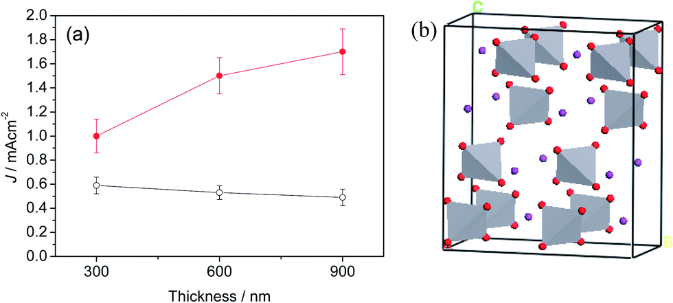 | ||
| Fig. 3 (a) Thickness dependence of the performance of planar BiVO4 and BiVO4/io-AZO heterostructure electrodes. The photocurrent densities were measured at 1.23 V vs. RHE. (b) Crystal structure of BiVO4, purple ball represents Bi and red ball is O. | ||
To further confirm the charge-collecting improvement of the AZO inverse opal network, electrochemical impedance spectroscopy (EIS) studies are carried out at 1.23 V vs. RHE to investigate the impedance across the interface between BiVO4 and AZO inverse opal networks. A sinusoidal alternating-current (AC) perturbation of 5 mV was applied to the electrode over the frequency range of 0.1 to 65000 Hz, and the impedance changes in response to the perturbation were measured. The EIS of planar BiVO4 films and BiVO4/io-AZO heterostructures are plotted in the form of a Nyquist plot and displayed in Fig. 4. An equivalent circuit (inset of Fig. 4a) based on a mid-gap charge carrier trapping mechanism,35 was employed to analyze the data. In the employed equivalent circuit, R1 is the series resistance (including the resistance between BiVO4 and io-AZO), R2 is the resistance to trapping/detrapping electrons in/out of the mid-gap state, R3 represents the charge transfer resistance at the interface, whereas C is the capacitance of the space-charge region and Q represents the constant phase element. The fitted R1 for the planar BiVO4 films and BiVO4/io-AZO heterostructures are 99 ± 2 and 42 ± 3 Ω, respectively. The small series resistance in BiVO4/io-AZO suggests efficient charge transfer from BiVO4 to the charge collecting io-AZO network. A lower value of R3 suggests more efficient charge transfer across the electrode/electrolyte interface, reducing the possibility of charge recombination and thus enhancing the photocurrent response.36 The fitted R3 values for planar BiVO4 films and BiVO4/io-AZO heterostructures are 9200 ± 60 and 1560 ± 10 Ω, respectively. The charge transfer resistance is 83% lower in BiVO4/io-AZO than planar BiVO4, indicating that the BiVO4/io-AZO heterostructure possesses more efficient charge transfer than that of the bare BiVO4 film due to the existence of the conductive charge collecting network.
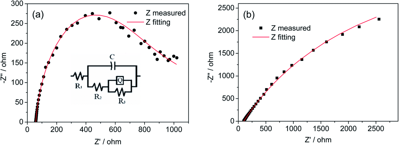 | ||
| Fig. 4 Nyquist EIS plots of (a) BiVO4/io-AZO heterostructure and (b) planar BiVO4 without io-AZO framework. The inset of (a) is the equivalent circuit used to analyze the data, the red solid line is the fitted curve based on the proposed equivalent circuit. | ||
The incident photon-to-charge conversion efficiencies (IPCEs) of the planar BiVO4 film and BiVO4/io-AZO heterostructure are measured and plotted as a function of wavelength, as shown in Fig. 5. The IPCE spectra of the planar and heterostructure electrodes both exhibit photoresponse up to 530 nm, as expected from the absorption edge of BiVO4. For both electrodes, the maximum IPCE is achieved at 420 nm with 11.6% and 30.7% for the planar and BiVO4/io-AZO electrode, respectively. We emphasize that the performance of the BiVO4/io-AZO heterostructure is almost three times as high as that of the planar BiVO4 film, suggesting the introduction of conductive inverse opal networks into the BiVO4 film significantly improve the IPCE. A comparison of the UV-Vis absorbance spectra (Fig. S1† in ESI) of the planar BiVO4 and BiVO4/io-AZO heterostructure electrodes reveal that light absorption is enhanced by approximately 10% at 450 nm in the BiVO4/io-AZO heterostructure electrode compared to planar BiVO4, which may be attributed to light scattering within the io-AZO inverse opal network. This enhanced light absorption may also contribute to a small extent to the improved photocurrent. The heterostructure displays good photostability and the photocurrent only decreased by 6% at an applied potential of 1.23 V vs. RHE after 4 hours photoelectrochemical water splitting (see Fig. S2† in the ESI).
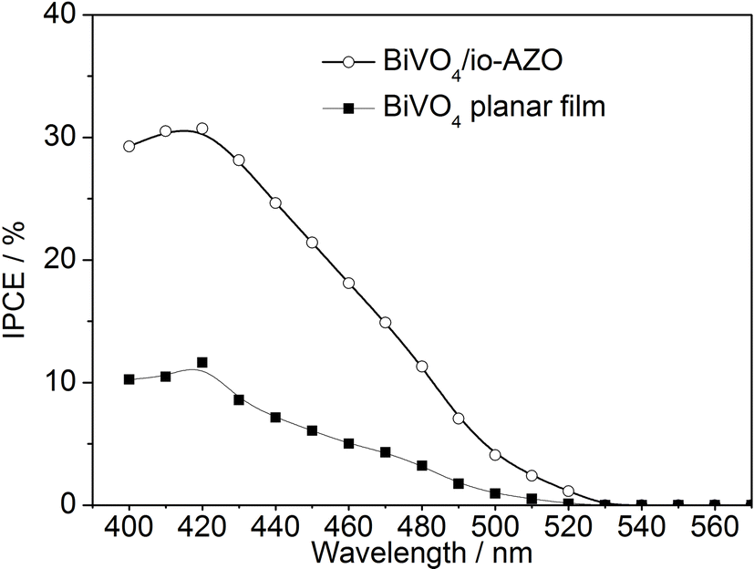 | ||
| Fig. 5 IPCE of BiVO4/io-AZO heterostructure and planar BiVO4 without io-AZO. | ||
In conclusion, to address the photogenerated electron transport problems in BiVO4 photoanodes, an inverse opal structured Al-doped ZnO network with continuous pores and good conductivity is prepared and employed as charge transporter in BiVO4 photoanodes to improve charge collection. The BiVO4/io-AZO heterostructure shows a photocurrent of 1.5 mA cm−2 at 1.23 V vs. RHE, which is a threefold enhancement compared to that of planar BiVO4 photoanodes. The introduction of the conducting io-AZO network into BiVO4 thereby significantly improves the charge collection in the BiVO4/io-AZO hybrid photoelectrode. Our approach has wide potential to be applied to other solar fuels systems to improve charge collection and solar energy conversion efficiency.
Experimental
Synthesis of AZO inverse opal
Monodisperse PS (polystyrene) spheres with diameters of 320 nm (Sigma-Aldrich Chemie Gmbh) were diluted with deionized water to 0.2 wt%. The FTO glass slide was held vertically in a 10 mL vial containing the suspension of the monodisperse PS spheres (320 nm diameter). As the water evaporates and the meniscus sweeps down the substrate and capillary forces induce ordering of the spheres on the surface of the FTO glass slide.The precursor for AZO was prepared by dissolving 0.02 mol zinc acetate dihydrate and 6 × 10⁻⁴ mol aluminium nitrate in 100 mL deionized water. To achieve a homogeneous infiltration of the transparent precursor into opal template, dip-coating infiltration was employed. The FTO glass with opal template was dipped into the precursor, and this process repeated until the template was well infiltrated with the precursor. Finally, the templates and organic components in the precursor were removed by heating at 450 °C for 3 hours in air.
Synthesis of BiVO4/io-AZO heterostructure
The BiVO4 precursor solution used for the infiltration of the void volume of the io-AZO is produced as follows: 0.02 mol of diethylenetriaminepenta-acetic acid (H5DTPA) and 7.5 mL ammonia in water (13.0 mol L−1) were added to 200 mL hot distilled water. After dissolution, 10 mmol of Bi(NO3)3 (Sigma-Aldrich) and 4.850 mmol of V2O5 powder (Sigma-Aldrich) were added. The resulting mixture was stirred and heated at 80 °C to promote complexation of Bi3+ and V5+ with DTPA and formation of a transparent solution.The as-prepared io-AZO was dipped into the precursor, and this process repeated until the io-AZO was well infiltrated with the precursor. Then BiVO4 is formed from the precursor and crystallized by heating at 500 °C for 3 hours in air. A planar BiVO4 with a comparable thickness was prepared for comparison employing the same method but without io-AZO network.
Photoelectrochemical measurement
Photoelectrochemical measurements were carried out on an electrochemical workstation (IVIUMSTAT). A conventional three electrodes configuration was used with BiVO4, Pt wire and Ag/AgCl electrode as working electrode, counter electrode and reference electrode, respectively. The electrolyte was an aqueous phosphate buffer at pH 7. The working electrodes were illuminated from the back side unless otherwise noted. The light source is a 100 mW cm−2 solar light simulator equipped with an air mass 1.5 global filter and an IR water filter (Newport Oriel, 150 W). For IPCE measurements an Oriel Cornerstone 130 monochromator was used. All the potentials are reported against the reversible hydrogen electrode (RHE) by using the equation E (V vs. RHE) = E (V vs. Ag/AgCl) + 0.059 pH + 0.197. The software ZSimpWin was employed to analyze the EIS data.Acknowledgements
This work was financially supported by the UK Engineering and Physical Science Research Council (EP/H00338X/2 to E.R., EP/G060649/1 to J.J.B.), the Christian Doppler Research Association (Austrian Federal Ministry of Economy, Family and Youth and National Foundation for Research, Technology and Development), the OMV Group (to E.R.), a Marie Curie Intra-European Fellowship (FP7-PEOPLE-2011-IEF 298012 to L.Z.) and the ERC (ERC LINASS 320503 to J.J.B.).Notes and references
- M. Pagliaro, A. G. Konstandopoulos, R. Ciriminna and G. Palmisano, Energy Environ. Sci., 2010, 3, 279–287 CAS.
- P. D. Tran, L. H. Wong, J. Barber and J. S. C. Loo, Energy Environ. Sci., 2012, 5, 5902–5918 CAS.
- S. Bensaid, G. Centi, E. Garrone, S. Perathoner and G. Saracco, ChemSusChem, 2012, 5, 500–521 CrossRef CAS PubMed.
- A. Paracchino, V. Laporte, K. Sivula, M. Grätzel and E. Thimsen, Nat. Mater., 2011, 10, 456–461 CrossRef CAS PubMed.
- A. J. Cowan, C. J. Barnett, S. R. Pendlebury, M. Barroso, K. Sivula, M. Grätzel, J. R. Durrant and D. R. Klug, J. Am. Chem. Soc., 2011, 133, 10134–10140 CrossRef CAS PubMed.
- A. Kay, I. Cesar and M. Grätzel, J. Am. Chem. Soc., 2006, 128, 15714–15721 CrossRef CAS PubMed.
- K. Sivula, F. Le Formal and M. Grätzel, ChemSusChem, 2011, 4, 432–449 CrossRef CAS PubMed.
- G. Wang, Y. Ling, D. A. Wheeler, K. E. N. George, K. Horsley, C. Heske, J. Z. Zhang and Y. Li, Nano Lett., 2011, 11, 3503–3509 CrossRef CAS PubMed.
- D. K. Zhong and D. R. Gamelin, J. Am. Chem. Soc., 2010, 132, 4202–4207 CrossRef CAS PubMed.
- A. Walsh, Y. Yan, M. N. Huda, M. M. Al-Jassim and S. H. Wei, Chem. Mater., 2009, 21, 547–551 CrossRef CAS.
- L. W. Zhang, C. Baumanis, L. Robben, T. Kandiel and D. Bahnemann, Small, 2011, 7, 2714–2720 CrossRef CAS PubMed.
- A. Kudo, K. Ueda, H. Kato and I. Mikami, Catal. Lett., 1998, 53, 229–230 CrossRef CAS.
- A. Kudo, K. Omori and H. Kato, J. Am. Chem. Soc., 1999, 121, 11459–11467 CrossRef CAS.
- R. G. Li, F. X. Zhang, D. G. Wang, J. X. Yang, M. R. Li, J. Zhu, X. Zhou, H. X. Han and C. Li, Nat. Commun., 2013, 4, 1432 CrossRef PubMed.
- H. Ye, J. Lee, J. S. Jang and A. J. Bard, J. Phys. Chem. C, 2010, 114, 13322–13328 CAS.
- S. Kohtani, M. Tomohiro, K. Tokumura and R. Nakagaki, Appl. Catal., B, 2005, 58, 265–272 CrossRef CAS PubMed.
- Q. Jia, K. Iwashina and A. Kudo, Proc. Natl. Acad. Sci. U. S. A., 2012, 109, 11564–11569 CrossRef CAS PubMed.
- W. Luo, Z. Yang, Z. Li, J. Zhang, J. Liu, Z. Zhao, Z. Wang, S. Yan, T. Yu and Z. Zou, Energy Environ. Sci., 2011, 4, 4046–4051 CAS.
- K. J. McDonald and K.-S. Choi, Energy Environ. Sci., 2012, 5, 8553–8557 CAS.
- S. K. Pilli, T. E. Furtak, L. D. Brown, T. G. Deutsch, J. A. Turner and A. M. Herring, Energy Environ. Sci., 2011, 4, 5028–5034 CAS.
- L. Tong, A. Iwase, A. Nattestad, U. Bach, M. Weidelener, G. Götz, A. Mishra, P. Bäuerle, R. Amal, G. G. Wallace and A. J. Mozer, Energy Environ. Sci., 2012, 5, 9472–9475 CAS.
- F. F. Abdi, L. Han, A. H. M. Smets, M. Zeman, B. Dam and R. van de Krol, Nat. Commun., 2013, 4, 2195 Search PubMed.
- W. J. Jo, J.-W. Jang, K.-J. Kong, H. J. Kang, J. Y. Kim, H. Jun, K. P. S. Parmar and J. S. Lee, Angew. Chem., Int. Ed., 2012, 51, 3147–3151 CrossRef CAS PubMed.
- K. P. S. Parmar, H. J. Kang, A. Bist, P. Dua, J. S. Jang and J. S. Lee, ChemSusChem, 2012, 5, 1926–1934 CrossRef CAS PubMed.
- D. K. Zhong, S. Choi and D. R. Gamelin, J. Am. Chem. Soc., 2011, 133, 18370–18377 CrossRef CAS PubMed.
- H. S. Park, K. E. Kweon, H. Ye, E. Paek, G. S. Hwang and A. J. Bard, J. Phys. Chem. C, 2011, 115, 17870–17879 CAS.
- Y. Liang, T. Tsubota, L. P. A. Mooij and R. van de Krol, J. Phys. Chem. C, 2011, 115, 17594–17598 CAS.
- L.-W. Zhang, Y.-J. Wang, H.-Y. Cheng, W.-Q. Yao and Y.-F. Zhu, Adv. Mater., 2009, 21, 1286–1290 CrossRef CAS.
- S. Stoughton, M. Showak, Q. Mao, P. Koirala, D. A. Hillsberry, S. Sallis, L. F. Kourkoutis, K. Nguyen, L. F. J. Piper, D. A. Tenne, N. J. Podraza, D. A. Muller, C. Adamo and D. G. Schlom, APL Mater., 2013, 1, 042112 CrossRef PubMed.
- L. Chen, E. Alarcón-Lladó, M. Hettick, I. D. Sharp, Y. Lin, A. Javey and J. W. Ager, J. Phys. Chem. C, 2013, 117, 21635–21642 CAS.
- F. F. Abdi, T. J. Savenije, M. M. May, B. Dam and R. van de Krol, J. Phys. Chem. Lett., 2013, 4, 2752–2757 CAS.
- R. v. d. Krol and M. Grazel, Photoelectrochemical Hydrogen Production, Springer, 2012 Search PubMed.
- A. Hagfeldt, H. Lindstroem, S. Soedergren and S.-E. Lindquist, J. Electroanal. Chem., 1995, 381, 39–46 Search PubMed.
- N. J. Bell, Y. H. Ng, A. Du, H. Coster, S. C. Smith and R. Amal, J. Phys. Chem. C, 2011, 115, 6004–6009 CAS.
- K. J. Pyper, J. E. Yourey and B. M. Bartlett, J. Phys. Chem. C, 2013, 117, 24726–24732 CAS.
- S. J. Hong, S. Lee, J. S. Jang and J. S. Lee, Energy Environ. Sci., 2011, 4, 1781–1787 CAS.
Footnote |
| † Electronic supplementary information (ESI) available. See DOI: 10.1039/c3ee44031a |
| This journal is © The Royal Society of Chemistry 2014 |