 Open Access Article
 This Open Access Article is licensed under a Creative Commons Attribution-Non Commercial 3.0 Unported Licence
Dye sensitized solar cells as optically random photovoltaic media†
Francisco Enrique
Gálvez
a,
Piers R. F.
Barnes
c,
Janne
Halme
b and
Hernán
Míguez
*a
aMultifunctional Optical Materials Group, Instituto de Ciencia de Materiales de Sevilla, Consejo, Superior de Investigaciones Científicas-Universidad de Sevilla(US-CSIC), Américo Vespucio 49, 41092 Sevilla, Spain. E-mail: h.miguez@csic.es
bDepartment of Applied Physics, Aalto University School of Science, P.O. Box 15100, FI-00076, Aalto, Finland
cDepartment of Physics, Imperial College London, South Kensington Campus, London SW7 2AZ, UK
First published on 11th November 2013
Abstract
In order to enhance optical absorption, light trapping by multiple scattering is commonly achieved in dye sensitized solar cells by adding particles of a different sort. Herein we propose a theoretical method to find the structural parameters (particle number density and size) that optimize the conversion efficiency of electrodes of different thicknesses containing spherical inclusions of diverse composition. Our work provides a theoretical framework in which the response of solar cells containing diffuse scattering particles can be rationalized. Optical simulations are performed by combining a Monte Carlo approach with Mie theory, in which the angular distribution of scattered light is accounted for. Several types of scattering centers, such as anatase, gold and silver particles, as well as cavities, are considered and their effect compared. Estimates of photovoltaic performance, insight into the physical mechanisms responsible for the observed enhancements, and guidelines to improve the cell design are provided. We discuss the results in terms of light transport in weakly disordered optical media and find that the observed variations between the optimum scattering configurations attained for different electrode thicknesses can be understood as the result of the randomization of the light propagation direction at different depths within the active layer. A primary conclusion of our study is that photovoltaic performance is optimised when the scattering properties of the film are adjusted so that the distance over which incident photons are randomized is comparable to the thickness of the film. This simple relationship could also be used as a design rule to attain the optimum optical design in other photovoltaic materials.
Broader contextOptical disorder is often introduced in dye solar cells to improve their efficiency as a result of the increased light harvesting that photon trapping gives rise to. Most of the time, the type of disorder actually introduced is based on practical considerations, such as the commercial products available, and empirical analysis, rather than on modelling of precise structures and their optical effects. This is a consequence of the complexity involved in preparing and describing theoretically well-defined disordered materials. In our work, we find a simple way to simulate the effect of disorder on the performance of dye solar cells considering realistic available materials, which allows us to both propose optimized configurations and find a design rule based on the concept of light randomization within the electrode. |
Introduction
Since its discovery in 19911 by O'Regan and Grätzel, the dye-sensitized solar cell (DSC), an electrochemical nanostructured device, environmentally gentle, economically promising, and rich in operational mechanisms, has been an object of intense research. Current laboratory devices can reach record efficiencies above 12%.2 Optimization of cell design also includes that of light harvesting efficiency, defined as the fraction of the incident photons that are absorbed by dye molecules sensitizing the nanocrystalline titania film. To achieve this, an increase of electrode thickness is discouraged since it implies an increased probability of recombination for conducting electrons due to the longer distance they need to travel to reach the collection point. Successful strategies have been developed based on the use of dye molecules with a spectrally wider absorption band and high molar extinction coefficient.3 Complementary or alternative to this approach is one that includes optical elements within the cell to either prevent unabsorbed light from escaping or to increase the optical path or electromagnetic energy density locally in the electrode. In DSCs, the most widely used dye, N719, absorbs weakly at the longer wavelengths of the visible spectrum. In the last decade, photonic crystal mirrors coupled to the electrode have been demonstrated to improve the performance of DSCs by enhancing the absorption of reflected photons while partially preserving their optical transparency, thus maintaining interest in the device for building integration.4–9 Diffuse scattering design also gives rise to an increase of the optical path length either by diffusely reflected light10–14 or by multiple scattering within the absorbing electrode.13,15–19 The former approach is based on the deposition of a layer of large (on the order of hundreds of nanometers) titania particles that behave as a diffuse back reflector, while the latter takes advantage of embedded scattering centers within the photoanode, which can be done either by admixing inorganic particles15–17 or organic ones18,19 that will yield cavities after calcination. Already successfully tested in other solar cells,20 plasmonic structures offer the possibility of guiding and trapping light by scattering as well as by near-field enhancement effects.21 Recently, several papers have reported an improvement of DSC performance by embedding gold and silver nanoparticles, be they bare or covered with an insulating shell.22–27Even though diffuse scattering layers attached at the back of the active area have been proven to provide the largest reinforcements of optical absorption, and actually all record cells have taken advantage of this effect, the scattering particles admixed with the paste offer two advantages of great interest. The first is avoiding the additional steps of fabrication and attachment of the scattering layer. The second is that diffuse back reflectors or photonic crystals are of no use in DSCs that operate under counter electrode illumination conditions, as it happens for cells fabricated on stainless steel substrates which are flexible and thus candidates for up-scaling and mass production.28 Additionally, the use of cavities offers the possibility of improving the electrolyte transport through the electrode, which may be a great advantage when high viscosity electrolytes, capable of raising the open circuit voltage, are employed. Cavities may also help the infiltration of hole transporting materials into the nanocrystal pores in solid state DSCs.
Tools to simulate, assess and optimize the light harvesting due to scattering in photoactive films have potential applications beyond DSCs. For example, extremely thin absorber cells, semiconductor sensitized solar cells and many photoelectrodes for solar fuel production exhibit strong scattering although there are currently few good approaches for estimating the optical absorption profile. A knowledge of these absorption profiles is generally critical for understanding the device function on a practical level. From a theoretical perspective, seminal computational studies by Ferber et al. and Usami implemented Mie theory in a radiative transfer based approach29 and a Monte Carlo method of multiple scattering,30 respectively. It was found that the benefit attained from embedding large TiO2 spherical scattering centres overcomes the associated drop in dye-loading, and estimations of the optimum particle size and load were provided. Also, Rothenberger et al. applied a semi-empirical four flux model to explain diffuse scattering effects in DSCs.31 In a recent paper,32 we analysed the effect of considering isotropic scattering by individual scatterers, which fairly accounts for the effect of actual commercial scattering paste, since the inclusions are usually broad size distribution polyhedra, which have been shown to display quite isotropic scattering.33 All scattering effects were determined by a single input parameter, the scattering mean free path. Interestingly, in good agreement with experimental observations, our work predicted a clear prevalence of designs in which a diffuse back scattering layer is coupled to the standard semitransparent electrode over those in which isotropic scattering particles are dispersed in the nanocrystalline titania paste. Our work also highlighted the importance of the interplay between the effect of the diffuse scattering design, the electron diffusion length and the electrode thickness, showing that different optical designs give rise to very different spatial distributions of optical absorption and therefore electron generation functions, thus affecting the electron collection efficiency. In general, the importance of an optoelectronic model of the DSCs is now being realized and addressed from different perspectives.34 More recently, the importance of the optical absorption profile on the collection efficiency has been further highlighted in nanostructured electrodes in which gaussian shape electron generation functions were considered.35
Herein we simulate the effect of the scattering caused by randomly distributed spherical inclusions of different kinds (titania, cavities, metallic beads) on the optical absorption, and hence photovoltaic performance, of a dye sensitised electrode. A Monte Carlo method in which the angular probability of scattering is weighted by the results of Mie scattering calculations is employed. The diameter, refractive index and concentration of scatterers are fully accounted for. Results of the optical modelling are used as an input for an electrical model based on a continuity equation for conduction band electron transport with sublinear recombination, from where we obtain all relevant photovoltaic parameters. Our motivation is two-fold: first, from a fundamental point of view, to establish a correlation between the key parameters typically employed to describe optically random media, i.e. scattering and transport mean free paths, and the improved conversion efficiency predicted; also, to provide an integral theoretical framework in which the performance of all types of currently proposed spherical scatterers can be compared. We find that the optimum set of particle parameters (size, refractive index, concentration) depends strongly on the electrode thickness considered. Optimization is driven by the balance between light randomization at the required depth in the photovoltaic material and the losses (observed as diffuse transmittance and reflectance, or parasitic absorption in the case of metals) optical disorder gives rise to. A main conclusion, consistent across the materials studied here, is that the scattering design optimizing the device performance achieves randomization of light propagation on a length scale on the order of the electrode thickness. In other words, the magnitude of the so-called transport mean free path, which is defined as the average distance over which the direction of propagation of a photon is randomized,36 should be approximately equal to the electrode thickness. This simple relationship could be used as a design rule to attain the optimum optical design of any random photovoltaic material, as well as a simple design rule to maximize light absorption.
Optical scattering model
To start with, spectral light harvesting efficiency, ηLH(λ), and optical absorption profile functions, g(x, λ), were calculated for the DSCs embedding different types of dispersed spherical scattering particles. We have employed a Monte Carlo approach to simulate the trajectory of 107 photons that enter the different cells under consideration. In this approximation, we are assuming Mie effects arising from the scattering of photons with wavelengths similar to the size of the particles, which yields highly anisotropic angular distributions.In our optical model, the incident beam is described as a collection of individual photons. Once a photon enters the cell, the distance travelled before experiencing either absorption or scattering,  , is given by the expression
 | (1) |
| αext = αsc + αA, | (2) |
| αsc = ρσsc, | (3) |
| αA = αA,dye + αA,elec + αA,part | (4) |
Please notice that the only optical losses contributing to photocurrent are those resulting from light harvesting occurring at dye molecules, while absorption occurring in the electrolyte or particles is unproductive. The absorption coefficient of the particles is given by
| αA,part = ρσA, | (5) |
If  attained from eqn (1) is longer than the electrode thickness, d, then the photon is ballistically transmitted or back reflected as explained below. If
  < d then a new random number, r′, is generated. If r′ ≤ αsc/(αA + αsc), the photon is scattered; for αsc/(αA + αsc) < r′ ≤ (αsc + αdye)/(αA + αsc), it is absorbed by the dye, thus generating charges capable of contributing to the photocurrent; for (αsc + αdye)/(αA + αsc) ≤ r′, the photon is captured either by the electrolyte or by the metal particle and then lost. The relative contribution to parasitic absorption of each one of these components can also be estimated by following a similar procedure. After a scattering event occurs, the new direction (ϕ, θ) of the propagating photon is determined by taking into account the numerically calculated angular distribution of scattered radiation attained from Mie theory.37
Finally, if a photon reaches the TCO outer surface, or any of the interfaces between the dyed TiO2 film and the TCO or the electrolyte, it has a certain probability of being back-reflected into the photoanode according to Fresnel coefficients. As has been pointed out by Usami, the presence of flat interfaces gives rise to confinement by total internal reflection that largely contributes to light harvesting. In our case, we assume that only the air–TCO and the TCO–nanocrystalline TiO2 edges are flat. The effect of the roughness at the tens of nanometers length scale, typically observed for the back surface of printed TiO2 electrodes (that is, the electrode–electrolyte interface), is accounted for by simulating a gradual decrease of refractive index as light enters the electrolyte layer.
All these possible events are considered until the photon escapes the cell, is removed by parasitic losses, or is productively absorbed by the dye at a specific depth in the electrode. In this way, light harvesting spatial profiles are obtained and serve as electron generation rate functions, G(x), (illustrative examples are provided in Fig. S1, as well as a drawing of the simulated cell in Scheme S1†) for a conduction band electron density continuity equation with sublinear recombination, which we use to calculate the energy conversion efficiency, as explained in the next section. It should be noticed that such electron generation rate functions strongly deviate from those derived from the Lambert–Beer law, applicable only to semi-transparent electrodes. This has a significant impact on the electron collection efficiency for those cells in which electron diffusion is somewhat hindered,32 not considered in the work herein presented.
Electrical model
Herein we use a state of the art electrical model based on a continuity equation in which multiple trapping electron transport kinetics38,39 and sublinear recombination are considered. In particular, we make use of a code developed by Barnes et al.40 For a thorough analysis of the validity and applicability of this model with respect to the standard one introduced by Södergren et al.,41 we refer the reader to the work by Bisquert et al.42 and Barnes et al.43 We note that the model explicitly assumes non-linearity in free electron recombination while free electron conduction is linear. Free electron transport may also be non-linear in many DSCs and either or both recombination and transport could contribute to the non-ideality of the observed photovoltaic characteristics.44,40 In this work it is sufficient to parameterise both these effects within the non-linearity of the recombination term to reproduce realistic current–voltage characteristics.Once the electrons are injected into the semiconductor conduction band, they must reach the contact in order to contribute to the photocurrent. Each individual electron does not feel the electric field caused by the imbalance between electrons and holes in the semiconductor or the reduced species of the electrolyte couple after dye-regeneration because both phases are interpenetrated in the nanometre scale and single phase charge imbalances are shielded. As a result, the driving force for the conduction is the gradient of the electron concentration of the conduction band through the photoanode and the transport is diffusive. In a nanocrystalline semiconductor, such transport is slowed by the presence of localized states with energy below the conduction band in which conduction electrons are trapped and released after some time. The equilibrium between the populations of trapped localized electrons and those free to move in the conduction band is reached instantaneously compared to the other characteristic times of phenomena occurring in a DSC. Transport properties in transient measurements depend on the sharpness of trap energy distribution and the amount of traps occupied. Sub-linear recombination can be explained by a fraction of the electrons recombining with the electrolyte from trap states localized at the surface of the particles in addition to those recombining from the conduction band. This recombination rate depends on the energy distribution of the states according to Marcus electron transfer theory.45 Electrons can also be lost by recombination with dye oxidized molecules but this effect typically plays a minor role and is not considered in this paper. Furthermore the effects of variations in the concentration profile of electron accepting ions in the electrolyte are also neglected; this effect which leads to spatial variations in kr could be significant in devices with high electrolyte viscosity or low photoanode porosity.
With the above assumptions the continuity equation adopts the shape:
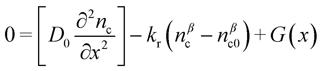 | (6) |
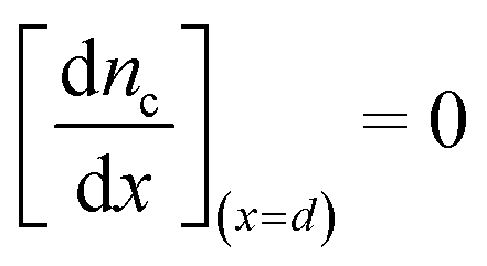 | (7) |
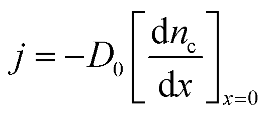
At the collection point, x = 0, the flux extracted and injected into the external circuit is proportional to the slope of the electron concentration:
 | (8) |
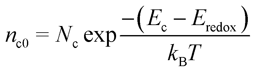
In turn, nc at the contact is determined by the voltage of the cell by the following expression, which considers the Boltzmann approximation:
 | (9) |
 | (10) |
The continuity equation, with the above boundary conditions, is solved using a parabolic elliptic partial differential equation MatLab solver40 for each one of the electron generation profiles obtained from the optical model. The cell current density is given by the electron flux at x = 0. The I–V curve can then be obtained by varying V between short circuit conditions (V = 0) and the value at which current density falls to zero, corresponding to open circuit conditions. The efficiency of the cell is obtained as the ratio between the incident solar energy and the maximum power provided by the cell.
Results and discussion
As an initial test of the validity of our optical scattering model we calculated the absorptance as a function of wavelength for two DSCs as described in ref. 13, using the reported fabrication details as input parameters to our model. In that paper, Arakawa et al. presented incident photon-to-electron conversion efficiency (IPCE) measurements for devices fabricated with and without the addition of scattering particles. The electron injection and collection efficiency in these devices was optimised to be close to 100% such that the resulting IPCE spectrum is expected to be approximately equivalent to the cell's absorptance spectrum. Fig. 1a shows the IPCE spectrum presented in ref. 13 for a cell sensitized with N719 dye with no scattering particles and a similar cell containing 40 wt% of 100 nm scattering particles. Fig. 1b shows the corresponding absorptance spectra calculated in this work. There is excellent quantitative agreement between the spectra. This gives confidence that the optical model results yield physically meaningful results. Below we present optoelectronic simulations to explore the influence of differing optical scatterers on the performance of DSCs.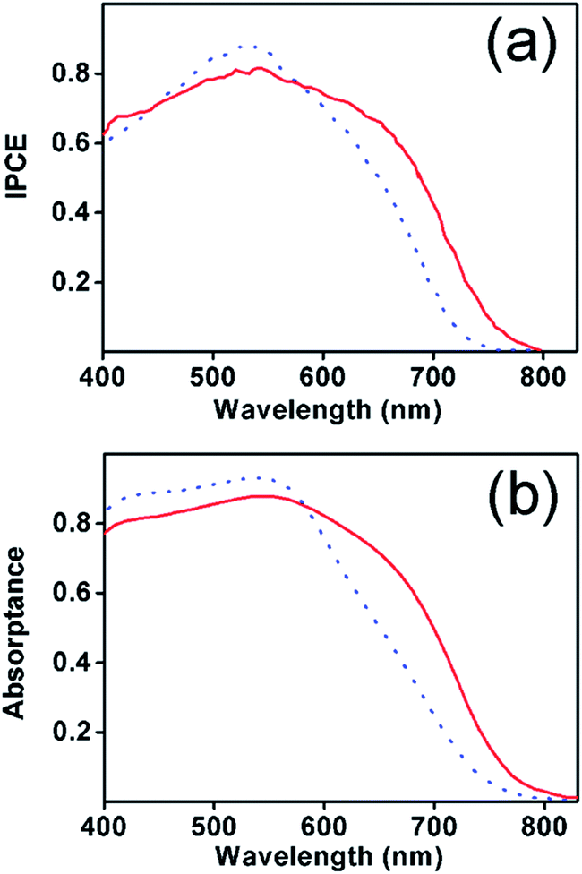 | ||
| Fig. 1 (a) Experimental IPCE as reported by Arakawa et al. in ref. 13 and (b) calculated optical absorptance as estimated with the theoretical model herein proposed. In our model, we use as input parameters the data reported in their manuscript (electrode thickness of 17.5 microns, 40 vol% particle concentration, and 100 nm diameter). | ||
The performance of solar cells made of nanocrystalline TiO2 electrodes with thickness comprised in the range 1 μm < d < 8 μm was simulated using the optical and electrical models described above. Spherical scattering centres consisting of anatase, gold, silver and holes filled with electrolyte, with diameters comprised between 20 and 400 nm and with volume fractions in the range 0 to 40%, were considered. Although they can be estimated from first principles,49,50 in this case the wavelength dependent refractive index and absorption coefficients employed for the calculations were extracted from the optical characterization of the electrodes51 and can be found in the ESI (Fig. S2†), along with the values of all relevant electrical parameters, which are consistent with those previously employed to simulate the performance of DSCs.40
Power conversion efficiency, η, maps as a function of radius, a, of the scatterers and the total volume occupied by them were attained. An illustrative example is shown in Fig. 2, which corresponds to electrodes of d = 8 μm respectively (results for electrodes of other thicknesses are provided in the ESI, Fig. S3–S5†). In all cases, the configuration that yields the highest cell performance was sought after. One of the first conclusions that could be extracted from this analysis is that, in all cases, it is possible to find conditions under which the scattering caused by the inclusions gives rise to better photovoltaic performance when compared to that of a reference cell (0% concentration in the efficiency maps). Please notice that the presence of scattering particles not only implies the removal of part of the light harvesting material (i.e., dyed nanocrystalline titania), but also concentrates the electrons generated within a smaller conducting volume, which raises nc, thus boosting the voltage logarithmically. Interestingly, in all cases, optimum performance occurs for a relatively broad range of sizes and concentrations, which implies that there is a high degree of tolerance to experimental deviations from a predetermined set of structural parameters. The results attained for the optimum particle radius and concentration for each type of embedded particle and electrode thickness are summarized in Table 1, in which the values of short circuit photocurrent, Isc, open circuit voltage, Voc, fill factor, FF, and conversion efficiency are shown.
 | ||
| Fig. 2 Power conversion efficiency versus sphere radius and volume fraction for electrodes of 8 micron thick electrodes including (a) titania, (b) electrolyte filled cavities, (c) gold, and (d) silver particles. | ||
| Material | Radius (nm) | Load (%V) | I sc (mA cm−2) | V oc (V) | FF (%) | Eff. (%) |
|---|---|---|---|---|---|---|
| Thickness 1 micron | ||||||
| None | — | — | 2.43 | 0.72 | 80 | 1.40 |
| Cavities | 95 | 32 | 4.05 | 0.75 | 81 | 2.45 |
| Anatase | 105 | 32 | 4.43 | 0.75 | 81 | 2.70 |
| Gold | 75 | 1.2 | 2.98 | 0.72 | 81 | 1.74 |
| Silver | 70 | 2.2 | 4.02 | 0.74 | 80 | 2.38 |
| Thickness 2 microns | ||||||
| None | — | — | 4.39 | 0.71 | 81 | 2.52 |
| Cavities | 100 | 32 | 7.29 | 0.75 | 81 | 4.41 |
| Anatase | 120 | 30 | 7.89 | 0.75 | 81 | 4.79 |
| Gold | 75 | 0.6 | 5.11 | 0.72 | 81 | 2.96 |
| Silver | 70 | 1.2 | 6.47 | 0.73 | 81 | 3.81 |
| Thickness 4 microns | ||||||
| None | — | — | 4.13 | 0.71 | 81 | 4.13 |
| Cavities | 110 | 30 | 11.11 | 0.74 | 81 | 6.67 |
| Anatase | 130 | 26 | 11.68 | 0.74 | 81 | 7.01 |
| Gold | 80 | 0.4 | 7.96 | 0.71 | 81 | 4.60 |
| Silver | 65 | 0.6 | 9.38 | 0.72 | 81 | 5.47 |
| Thickness 8 microns | ||||||
| None | — | — | 9.93 | 0.70 | 82 | 5.67 |
| Cavities | 115 | 24 | 13.86 | 0.72 | 82 | 8.17 |
| Anatase | 140 | 22 | 14.20 | 0.72 | 82 | 8.37 |
| Gold | 85 | 0.2 | 10.64 | 0.70 | 82 | 6.10 |
| Silver | 80 | 0.4 | 11.75 | 0.70 | 82 | 6.77 |
Regarding spherical dielectrics, we observe that dispersed cavities of the appropriate size and at the right concentration perform almost as well as anatase particles do, which open interesting possibilities since large spherical pores should also allow better flow of electrolyte species through the cell. This might also be of particular relevance for processing of cells using solid state electrolytes where infiltrating the hole conducting material into small pore sizes can be problematic. The possibility of achieving a similar performance with anatase particles and electrolyte filled cavities is somewhat surprising, since the scattering strength of TiO2 spheres (n = 2.5) is expected to be higher than that of electrolyte filled cavities (n = 1.42) when both are embedded in an electrolyte filled nanocrystalline titania medium (n = 1.96). The origin of the comparable magnitude of the enhancement effect caused by both types of particles is due to the different angular distribution of scattered light and is discussed below in detail. In both cases, an optimized DSC performance is found for inclusions of radius within the range 95 nm < a <140 nm, depending on the electrode thickness. The thicker the electrode, the larger the particle or cavity size that makes the cell efficiency maximum, and the lower the concentration required, which drops from around 30 vol% for 1 μm thick electrodes to around 20 vol% for the thickest electrodes considered.
In the case of metallic particles, a similar trend is observed. An optimized DSC performance is found for radii in the range 65 nm < a < 85 nm, with concentrations up to around 2 vol% for thin electrodes, and as low as 0.2 vol% for electrodes of standard thickness (4 μm to 8 μm). These low values of the optimum concentrations for both gold and silver are a constraint imposed by the presence of parasitic losses introduced by metal beads due to the absorption caused by excitation of localized surface plasmon modes. On the other hand, when results for metallic and dielectric particles are compared, it is immediately seen that the optimum scattering configurations provide significantly less improvement for the former than for the latter. This difference might be overcome by field enhancement effects that occur very close to the metal particle surface, not considered here but broadly investigated experimentally in different types of solar cells lately.21 Such effects are particularly intense for very small particles (r < 5 nm), although for them also parasitic absorption takes very high values (please see Fig. S6 in the ESI†) and scattering cross-section diminishes, which is actually the reason why poorer performance than the reference is found for the smaller size metal particles herein considered, irrespective of their concentration. Repeatedly reported experimental confirmation of photocurrent improvement of thin DSCs (d < 2 μm) caused by local field enhancement around very small metal inclusions seems to indicate that this effect is strong enough to surpass the competing losses caused by parasitic absorption or plasmon oscillation damping. However, the relative importance of the different optical and electrical effects that arise from the presence of metals within nanostructured electrodes is yet to be unveiled, as has been recently pointed out.52 Metallic particles may in some cases catalyse electron recombination with the electrolyte. A further concern is that metal particles are also susceptible of being corroded by the electrolyte, which implies that it may be necessary to coat them with a thin layer of dense metal oxide to include them in the electrode.22 Since the optical field intensity is maximum at the particle surface, such coating may render field enhancement effects, and hence the concomitant improvement of photovoltaic performance, significantly smaller.
Insight of the origin of the features and trends observed in the efficiency plots (as displayed Fig. 2 and S3–S5†) is provided by analysing the effect of concentration and particle size on the key parameters employed to describe light propagation in random media, namely the scattering mean free path, lsc, and the transport mean free path, lt.53–55 While the former corresponds to the average distance travelled by photons between two scattering events, the latter provides information on the average distance at which the direction of a propagating beam can be considered randomized. For diluted dispersions of scattering particles, like the ones herein assumed, phase correlations (i.e. wave interference effects) can be neglected. The particle density and scattering cross-section determine lsc, which is the inverse of the scattering coefficient defined in eqn (3), lsc = (ρσsc)−1, while lt depends on the angular distribution of a single scattering event. Both parameters are related by the scattering anisotropy parameter, g, through the formula56
 | (11) |
![[thin space (1/6-em)]](https://www.rsc.org/images/entities/char_2009.gif) θ〉 is the average of the cosine of the scattering angle, that is, the average weighted by the angular distribution of intensity provided by Mie theory, with θ measured from the direction of the incident beam. If isotropic scattering occurs,32 then g ≈ 0 and lt ≈ lsc and light transport can be considered diffusive after one scattering event. However, for spherical inclusions of size comparable to the wavelength, as is the case herein, the probability of scattering in the forward direction is high, which yields g closer to 1 and hence lt > lsc, implying that photons must be dispersed several times before the light beam direction becomes randomized.
θ〉 is the average of the cosine of the scattering angle, that is, the average weighted by the angular distribution of intensity provided by Mie theory, with θ measured from the direction of the incident beam. If isotropic scattering occurs,32 then g ≈ 0 and lt ≈ lsc and light transport can be considered diffusive after one scattering event. However, for spherical inclusions of size comparable to the wavelength, as is the case herein, the probability of scattering in the forward direction is high, which yields g closer to 1 and hence lt > lsc, implying that photons must be dispersed several times before the light beam direction becomes randomized.
In Fig. 3 and 4 we plot the spectral variation of the parameters Qsc, g, lsc and lt for the optimized configuration (particle size and concentration) attained for the different electrode thicknesses considered for titania and silver particles, respectively, which are selected as illustrative examples. Similar graphs for the two other particle types are provided as ESI (see Fig. S7 and S8†). Interestingly, for the case of titania, the optimum diffuse scattering design is that in which the randomization distance lt is on the order of or smaller than d in the spectral range 400 nm < λ < 650 nm, for which the dye absorption is significant. This relationship determines the observed trends for the optimum particle size and concentration with d: as the electrode becomes thinner, a wider angular distribution (that is, smaller value of g) of scattered light is required in order to randomize light at shorter depths. This is better achieved by small particles that, on the other hand, show lower scattering efficiency in the targeted spectral range (please see Qscvs. λ in Fig. 3a). Such reduced scattering is counterweighted by increasing particle concentration ρ, which then allows the reduction of lsc so that lt is shorter, i.e. light randomization occurs at a smaller depth. Similar conclusions can be extracted from the analysis of the same parameters for the optimized spherical cavities' size and concentration (Fig. S7†). As mentioned above, a similar cell performance is achieved with both kinds of dielectric scatterers at a relatively similar ρ value, even though Qsc of an electrolyte filled cavity is substantially smaller than that of a titania particle. In this case, a similar degree of light randomization at the right depth is attained by the effect of the angular distribution of the scattering angle, which is significantly broader for the case of light dispersed by electrolyte filled cavities. Please notice that for a given particle size, lsc and hence lt could always be made shorter at the expense of increasing ρ, but this would imply both reducing the total amount of dye and increasing reflectance losses, hence reducing the efficiency of the cell.
 | ||
| Fig. 3 (a) Scattering cross-section (Qsc), (b) scattering anisotropy parameter, g, (c) scattering mean free path (lsc), and (d) transport mean free path (lt), both in microns, for nanocrystalline titania electrodes including anatase particles as scatterers. Electrode thicknesses are d = 1 μm (red dotted line), d = 2 μm (green dashed line), d = 4 μm (blue dashed dotted line) and d = 8 μm (black solid line). The scattering particle size and concentration are such that they optimize light harvesting and thus power conversion efficiency in each case (see Table 1). | ||
 | ||
| Fig. 4 (a) Scattering and absorption cross-section (Qsc, Qa), (b) scattering anisotropy parameter, g, (c) scattering mean free path (lsc), and (d) transport mean free path (lt), both in microns, for nanocrystalline titania electrodes including silver particles. Electrode thicknesses are d = 1 μm (red dotted line), d = 2 μm (green dashed line), d = 4 μm (blue dashed dotted line) and d = 8 μm (black solid line). The particle size and concentration are such that they optimize light harvesting and thus power conversion efficiency in each case (see Table 1). | ||
For silver particles, Qsc takes higher values than for dielectric ones. However, lsc is always much longer for metal particles, as their optimum concentration is between one and two orders of magnitude smaller than that for dielectric particles, which is a direct consequence of their parasitic absorption. This is somewhat compensated by the broad angular distribution of light scattered by silver particles, as the low values of g indicate, which ends up resulting in lt values that are on the order of d in the targeted spectral range 500 nm < λ < 600 nm. The higher parasitic absorption of gold and its lower Qsc, in the range at which the N-719 dye used here absorbs (λ < 650 nm), results in an even lower optimum particle number density which, together with higher values of g, gives rise to lt much longer than d (see Fig. S8†). All this explains the poorer performance of gold particles as absorption enhancers when compared to silver beads.
Although the analysis of lsc and lt provides a description of the phenomena occurring within optically disordered photovoltaic materials, it is also helpful to introduce a parameter directly related to the enhancement of light–matter interaction that is ultimately responsible for the improvement of performance. Such a parameter is the average path lp, which we define as the mean length of the full trajectory travelled by photons within the electrode before escaping, being absorbed by the electrolyte or, in the case of gold and silver particles, being absorbed by the metal. Like lt and lsc, lp is estimated for the dye free media. As can be seen in Fig. 5, the optimized configurations give rise to average light path lengths between two (1 μm thick electrodes) and four (8 μm thick electrodes) times longer than the electrode thickness for the case of embedded dielectric scatterers. As expected, longer average photon trajectories are found for electrodes containing silver particles, in good agreement with the shorter light randomization lengths observed. The electrode thicknesses we have employed (1 μm, 2 μm, 4 μm and 8 μm) for our calculations are representative as most electrode widths employed lie within the 1–8 μm range. The comparative analysis of these four cases allows us to define clear trends that can be interpolated and extrapolated to explain the behaviour of electrodes of arbitrary thickness.
 | ||
| Fig. 5 Average path (lp) travelled by photons inside the different electrodes under consideration. Results are shown for nanocrystalline titania electrodes including (a) anatase particles, (b) electrolyte filled cavities, (c) gold particles, and (d) silver particles. Electrode thicknesses for which curves are plotted are d = 1 μm (red dotted line), d = 2 μm (green dashed line), d = 4 μm (blue dashed dotted line) and d = 8 μm (black solid line). The particle size and concentration are such that they optimize light harvesting and thus power conversion efficiency in each case (see Table 1). | ||
Conclusions
We have established a relationship between the structural features of optically disordered photovoltaic materials, such as dyed electrodes containing spherical scattering centres, with the relevant parameters that describe light propagation in random media, i.e., the scattering mean free path and the transport mean free path. We demonstrate that the optimized particle size and concentration, for dielectric and low absorption metal particles, are the ones that give rise to light randomization lengths, i.e., transport mean free paths, on the order of the electrode thickness. This conclusion is in principle independent of the type of photovoltaic material considered. A comparative analysis between the performance as efficiency enhancers of different types of dielectric and metallic scattering particles commonly employed in the field of dye sensitized solar cells yields that the former always performs better than the latter. The competing parasitic absorption of metal particles limits the maximum absorption enhancement that can be achieved and imposes a low particle number density in the electrode. Interestingly, as a consequence of the combined effect of both scattering intensity and its angular distribution, it is possible to achieve similar values of light randomization and hence the efficiency using different dielectrics of different refractive indices by adjusting the particle size and concentration. This opens the interesting possibility of using cavities rather than particles to enhance the conversion efficiency, which will improve electrolyte flow. Furthermore, this is the first time that a simple design rule has been proposed that allows mastering optical disorder in dye sensitized electrodes to achieve maximum efficiency. These methods and concepts may also apply to other photovoltaic devices, such as those based on extremely thin absorbers or on semiconductor sensitized photoconducting electrodes, as well as to photoelectrodes used for solar fuel production. We foresee further applications of this model in the development of advanced electrochromic windows, paints and papers.Acknowledgements
The research leading to these results has received funding from the European Research Council under the European Union's Seventh Framework Programme (FP7/2007–2013)/ERC grant agreement no. 307081 (POLIGHT), the Spanish Ministry of Economy and Competitiveness under grants MAT2011-23593 and CONSOLIDER HOPE CSD2007-00007, and the Junta de Andalucía under grants FQM3579 and FQM5247. PB is grateful to funding from the EPSRC APEX project (EP/H040218/1) and fellowship (EP/J002305/1).References
- B. O'Regan and M. Grätzel, Nature, 1991, 353, 737 CrossRef CAS.
- A. Yella, H. W. Lee, H. N. Tsao, C. Yi, A. K. Chandiran, M. K. Nazeeruddin, E. W.-G. Diau, C. Y. Yeh, S. M. Zakeeruddin and M. Grätzel, Science, 2011, 334, 629–634 CrossRef CAS PubMed.
- M. K. Nazeeruddin, P. Pechy, T. Renouard, S. M. Zakeeruddin, R. Humphry-Baker, P. Comte, P. Liska, L. Cevey, E. Costa, V. Shklover, L. Spiccia, G. B. Deacon, C. A. Bignozzi and M. Gratzel, J. Am. Chem. Soc., 2001, 123, 1613 CrossRef CAS PubMed.
- S. Colodrero, A. Forneli, C. López-López, L. Pellejà, H. Míguez and E. Palomares, Adv. Funct. Mater., 2012, 22, 1303 CrossRef CAS.
- C. T. Yip, H. Huang, L. Zhou, K. Xie, Y. Wang, T. Fenq, J. Li and W. Y. Tam, Adv. Mater., 2011, 23, 5624 CrossRef CAS PubMed.
- A. Mihi, C. Zhang and P. Braun, Angew. Chem., Int. Ed., 2011, 50, 5712 CrossRef CAS PubMed.
- S. Nishimura, N. Abrams, B. A. Lewis, L. I. Halaoui, T. E. Mallouk, K. D. Benkstein, J. van de Lagemaat and A. J. Frank, J. Am. Chem. Soc., 2003, 125, 6306 CrossRef CAS PubMed.
- S. Guldin, S. Huttner, M. Kolle, M. E. Welland, P. Müller-Buschbaum, R. H. Friend, U. Steiner and N. Tetreault, Nano Lett., 2010, 10, 2303 CrossRef CAS PubMed.
- S. Colodrero, A. Mihi, L. Häggman, M. Ocaña, G. Boschloo, A. Hagfeldt and H. Míguez, Adv. Mater., 2009, 21, 764 CrossRef CAS.
- S. Ito, S. M. Zakeeruddin, R. Humphry-Baker, P. Liska, R. Charvet, P. Comte, M. K. Nazeeruddin, P. Pechy, M. Takata, H. Miura, S. Uchida and M. Gratzel, Adv. Mater., 2006, 18, 1202 CrossRef CAS.
- A. G. Agrios, I. Cesar, P. Comte, M. K. Nazeeruddin and M. Grätzel, Chem. Mater., 2006, 18, 5395 CrossRef CAS.
- K. M. Lee, V. Suryanarayanan and K. C. Ho, Sol. Energy Mater. Sol. Cells, 2006, 90, 2398 CrossRef CAS PubMed.
- A. S. Wang, H. Kawauchi, T. Kashima and H. Arakawa, Coord. Chem. Rev., 2004, 248, 1381 CrossRef PubMed.
- F. Huang, D. Chen, X. L. Zhang, R. A. Caruso and Y. B. Cheng, Adv. Funct. Mater., 2010, 20, 1301 CrossRef CAS.
- C. J. Barbé, F. Arendse, P. Comte, M. Jirousek, F. Lenzmann, V. Shklover and M. Grätzel, J. Am. Ceram. Soc., 1997, 80, 3157 CrossRef.
- J. Xi, Q. Zhang, K. Park, Y. Sun and G. Cao, Electrochim. Acta, 2011, 56, 1960 CrossRef CAS PubMed.
- Z. Tian, H. Tian, X. Wang, S. Yuan, J. Zhang, X. Zhang, T. Yu and Z. Zou, Appl. Phys. Lett., 2009, 94, 031905 CrossRef PubMed.
- S. Hore, P. Nitz, C. Vetter, C. Prahl, M. Niggemann and R. Kern, Chem. Commun., 2005, 2011–2013 RSC.
- H. J. Koo, Y. J. Kim, Y. H. Lee, W. I. Lee, K. Kim and N. G. Park, Adv. Mater., 2008, 20, 195 CrossRef CAS.
- K. R. Catchpole and A. Polman, Opt. Express, 2008, 16, 21793 CrossRef CAS.
- H. A. Atwater and A. Polman, Nat. Mater., 2010, 9(3), 205–213 CrossRef CAS PubMed.
- M. B. Brown, T. Suteewong, R. S. S. Kumar, V. D'Innocenzo, A. Petrozza, M. M. Lee, U. Wiesner and H. J. Snaith, Nano Lett., 2011, 11, 438 CrossRef CAS PubMed.
- J. Qi, X. Dang, P. T. Hammond and A. M. Belcher, ACS Nano, 2011, 5(9), 7108 CrossRef CAS PubMed.
- W. Hou, P. Pavaskar, Z. Liu, J. Theiss, M. Aykol and S. B. Cronin, Energy Environ. Sci., 2011, 4, 4650–465 CAS.
- N. C. Jeong, C. Prasittichai and J. T. Hupp, Langmuir, 2011, 27, 14609 CrossRef CAS PubMed.
- M. Ihara, M. Kanno and S. Inoue, Physica E, 2010, 42, 2867–2871 CrossRef CAS PubMed.
- S. Lin, K. Lee, J. Wu and J. Wu, Appl. Phys. Lett., 2011, 99, 043306 CrossRef PubMed.
- G. Hashmi, K. Miettunen, T. Peltola, J. Halme, I. Asghar, K. Aitola, M. Toivola and P. Lund, Renewable Sustainable Energy Rev., 2011, 15, 3717 CrossRef CAS PubMed.
- J. Ferber and J. Luther, Sol. Energy Mater. Sol. Cells, 1998, 54, 265 CrossRef CAS.
- A. Usami, Sol. Energy Mater. Sol. Cells, 2000, 64, 73 CrossRef CAS.
- G. Rothenberger, P. Comte and M. Grätzel, Sol. Energy Mater. Sol. Cells, 1999, 58, 321 CrossRef CAS.
- F. J. Gálvez, E. Kemppainen, H. Míguez and J. Halme, J. Phys. Chem. C, 2012, 116, 11426 Search PubMed.
- C. Hrelescu, T. K. Sau, A. L. Rogach, F. Jäckel, G. Laurent, L. Douillard and F. Charra, Nano Lett., 2011, 11, 402 CrossRef CAS PubMed.
- S. Wenger, M. Schmid, G. Rothenberger, A. Gentsch, M. Grätzel and J. O. Schumacher, J. Phys. Chem. C, 2011, 115, 10218–10229 CAS.
- J. P. González-Vázquez, G. Bigeriego and J. A. Anta, Mol. Simul., 2012, 38, 1242 CrossRef.
- P. D. Kaplan, A. D. Dinsmore, A. G. Yodh and D. J. Pine, Phys. Rev. E: Stat. Phys., Plasmas, Fluids, Relat. Interdiscip. Top., 1994, 50, 4827 CrossRef CAS.
- C. F. Bohren and D. R. Huffman, Absorption and Scattering of Light by Small Particles, John Wiley & Sons, 1983 Search PubMed.
- J. Bisquert and V. S. Vikhrenko, J. Phys. Chem. B, 2004, 108, 2313–2322 CrossRef CAS.
- J. Bisquert, J. Phys. Chem. B, 2004, 108, 2323–2332 CrossRef CAS.
- P. R. F. Barnes, A. Y. Anderson, J. R. Durrant and B. C. O'Regan, Phys. Chem. Chem. Phys., 2011, 13, 5798–5816 RSC.
- S. Södergren, A. Hagfeldt, J. Olsson and S. Lindquist, J. Phys. Chem., 1994, 98, 5552 CrossRef.
- J. Bisquert and I. Mora-Seró, J. Phys. Chem. Lett, 2010, 1, 450–456 CrossRef CAS.
- P. R. F. Barnes and B. O'Regan, J. Phys. Chem. C, 2010, 114, 19134–19140 CAS.
- P. R. F. Barnes, K. Miettunen, X. Li, A. Y. Anderson, T. Bessho, M. Grätzel and B. C. O'Regan, Adv. Mater., 2013, 25, 1881–1922 CrossRef CAS PubMed.
- Q. Wang, S. Ito, M. Grätzel, F. Fabregat-Santiago, I. Mora-Seró, J. Bisquert, T. Bessho and H. Imai, J. Phys. Chem. B, 2006, 110, 19406 CrossRef PubMed.
- L. M. Peter, J. Phys. Chem. C, 2007, 111, 6601–6612 CAS.
- A. Hagfeldt, G. Boschloo, L. Sun, L. Kloo and H. Pettersson, Chem. Rev., 2010, 110, 6595–6663 CrossRef CAS PubMed.
- H. Reiss, J. Phys. Chem., 1985, 89, 3783–3791 CrossRef CAS.
- B. M. Wong, M. Piacenza and F. Della Sala, Phys. Chem. Chem. Phys., 2009, 11, 4498 RSC.
- T. Stein, L. Kronik and R. Baer, J. Chem. Phys., 2009, 131, 244119 CrossRef PubMed.
- J. Halme, P. Vahermaa, K. Miettunen and P. Lund, Adv. Mater., 2010, 22, E210 CrossRef CAS PubMed.
- H. Choi, W. T. Chen and P. Kamat, ACS Nano, 2012, 6, 4418 CrossRef CAS PubMed.
- A. Lagendijk and B. A. van Tiggelen, Phys. Rep., 1996, 270, 143 CrossRef CAS.
- P.-A. Lemieux, M. U. Vera and D. J. Durian, Phys. Rev. E: Stat., Nonlinear, Soft Matter Phys., 1998, 57, 4498 CrossRef CAS.
- M. Reufer, L. F. Rojas-Ochoa, S. Eiden, J. J. Sáenz and F. Scheffold, Appl. Phys. Lett., 2007, 91, 171904 CrossRef PubMed.
- P. D. Kaplan, A. D. Dinsmore, A. G. Yodh and D. J. Pine, Phys. Rev. E: Stat. Phys., Plasmas, Fluids, Relat. Interdiscip. Top., 1994, 50, 4827 CrossRef CAS.
Footnote |
| † Electronic supplementary information (ESI) available. See DOI: 10.1039/c3ee42587h |
| This journal is © The Royal Society of Chemistry 2014 |