
 Open Access Article
 This Open Access Article is licensed under a
 Creative Commons Attribution 3.0 Unported Licence
Facile synthesis of phosphine free ultra-small PbSe nanocrystals and their light harvesting studies in ETA solar cells†
Javeed
Akhtar
*ab,
Mateusz
Banski
c,
Mohammad Azad
Malik
d,
Neerish
Revaprasadu
e,
Artur
Podhorodecki
c and
Jan
Misiewicz
c
aDepartment of Physics, Polymers & Materials Synthesis (PMS) Lab, COMSATS, Institute of Information Technology, Park Road, Islamabad 44000, Pakistan
bDepartment of Chemistry, The University of Azad Jummu and Kashmir Muzaffrabad, Pakistan
cInstitute of Physics, Wroclaw University of Technology, Wybrzeze Wyspianskiego 27, Wroclaw, 50-370, Poland
dSchool of Chemistry and Materials Science Centre, The University of Manchester, Oxford Road, Manchester, M13 9PL, UK
eDepartment of Chemistry, University of Zululand, Private Bag X1001, KwaDlangezwa, 3880, South Africa. E-mail: javeedkt@gmail.com
First published on 4th September 2014
Abstract
Ultra-small PbSe nanocrystals (NCs) were synthesized via a ‘one-pot’ approach in olive oil as the reaction medium and capping agent. The optical spectra showed discernible blue shifts in the absorption band edges (570–780 nm) due to strong quantum confinement effects and photoluminescence (PL) spectra showed significant strong emission peaks in the range of 780–850 nm. The broad peaks in the powder X-ray diffraction (p-XRD) pattern indicate the ultra-small size of the as-prepared NCs. These NCs were used to construct an extremely thin absorber (ETA) solar device after surface modification. The preliminary results indicate their potential as light harvesting entities in nanostructure based solar cells.
Introduction
Lead chalcogenide nanocrystals (NCs) have been the focus of interest lately due to their enhanced optical properties in the visible and near infrared region of the solar spectrum.1–5 This key property has been particularly studied in solar cell devices as light harvesting materials.1–5 Another exciting feature of lead chalcogenide NCs stems from their ability to exhibit multiple exciton generation,6–8 also known as the carrier multiplication effect, potentially increasing the amount of energy generated from a high energy photon which thereby increases the AM 1.5 power conversion efficiency. Other notable applications of lead chalcogenide NCs include biological imaging/labeling, light emitting diodes and telecommunication.2,5,9Bulk lead selenide (PbSe) is a narrow bandgap (0.28 eV) material that has a large exciton Bohr radius of 23 nm and small effective masses for both holes and electrons.10,11 In 2001, Murray and co-workers12 reported the first successful synthesis of PbSe NCs, thereafter several modifications to the experimental procedure have been applied.10,11,13 Usually lead oleate and n-trioctylphosphine selenide (TOPSe) are used as lead and selenium reagents, respectively. One of the limitations of the method is the inconsistency and inability to produce small PbSe NCs.14,15 A huge motivation for smaller PbSe NC synthesis arises from recent studies, which showed that PbS NCs smaller than 3 nm overcome air sensitivity by forming different surface oxidation products due to their reduced faceting.16 Successful demonstrations of improved photovoltaic devices based on ultrasmall PbS and PbSe NCs have been reported.17–19 Thus, an efficient synthesis of PbSe NCs of diameter smaller than 3 nm is of high interest.
Efforts to produce small PbSe NCs include the introduction of diphenylphosphine (DPP) and 1,2-hexadecanethiol in the synthesis. However, these modifications were not able to produce small-sized PbSe NCs in high yields.15,18 Recently, several groups have highlighted the presence of dialkylphosphine impurities in 90% pure trioctylphosphine (TOP) used in most synthesis and their effect on the final product.15,20–22 Krauss and co-workers reported that pure tertiary phosphine selenide (e.g. TOPSe) was unreactive towards the lead oleate.22 Small quantities of secondary phosphines present as impurities in tertiary phosphines accounted for the poor reactivity and low yields. Replacing TOPSe with a secondary phosphine such as diphenylphosphine selenide (DPPSe) led to marked improvements in reactivity as well as reaction yields. However, with DPPSe, the control over PbSe NCs is poorly understood.22 It is worth mentioning that the commonly used phosphines such as TOP and n-tributylphosphine contain dioctylphosphine and dibutylphosphine as impurities, respectively.23 For a better control over ultrasmall PbSe NC synthesis, Alivisatos et al . have recently used bis(trimethylsilyl) selenide ((TMS)2Se) as a selenium source with lead oleate.24 The authors have explained that the formation of ultrasmall PbSe NCs is a result of (i) the highly reactive selenium precursor, (ii) the lower concentration of oleic acid and (iii) the high concentration of lead oxide during the synthesis. The used method is a slight modification of a previous synthetic route for producing PbS NCs using bis(trimethylsilyl) sulfide (TMS)2 as a sulfur source.25 We have reported homogeneous nanoalloys of PbSxSe1−x (x = 0–1) using (TMS)2S and (TMS)2Se.26 It was important to overcome the differences in reactivity of sulfur and selenium sources using reagents with similar structures and by inference reactivity. Herein we report the synthesis of ultrasmall PbSe NCs by a green route using olive oil.
In the first part of this work, we report detailed investigations on the optical properties of ultrasmall PbSe NCs (<3 nm) with interesting size dependent properties, prepared using a modified procedure.26,27 Low temperature annealing and the optical and structural properties of ultrasmall PbSe NCs are also demonstrated. In the second part, we demonstrate the potential of ca. 2 nm PbSe NCs in extremely thin absorber layer (ETA) solar cells in a ZnO–SnO2/In2S3/PbSeNCs/PEDOT:PSS configuration.28 In general, a typical ETA solar cell consists of a porous n-type semiconducting metal oxide anode to facilitate electron transport, a conformal light harvesting layer (known as the ETA layer), and a pore filling p-type semiconducting layer for hole transport. Similar to dye-sensitized solar cells, the process of light absorption is followed by charge separation and carrier transport.29 It is worth mentioning that the objectives of the composite metal oxide electrodes (ZnO–SnO2) as photoelectrodes are to enhance the key ETA cell properties such as open circuit voltage (Voc), short circuit photocurrent density (Jsc), and fill factor (FF).29 We show preliminary results of both modified and unmodified surfaces of PbSe NCs. To the best of our knowledge, this is the first example of PbSe NCs as an absorbing semiconductor in ETA solar cells.
Experimental section
Materials
All the chemicals were purchased from Sigma Aldrich Ltd, UK and used as received. Bis(trimethylsilyl) selenide ((TMS)2Se) was obtained from Gelest, Inc. All the solvents were dried prior to use. Olive oil (extra virgin) was purchased from Tesco supermarket, UK. Fluorine-doped tin oxide (FTO) coated glass substrates (TEC8, 8 Ω) were purchased from Pilkington. All the manipulations were carried out using standard Schlenk line techniques.Synthesis of PbSe nanocrystals
PbO (0.90 g, 4 mmol) was dissolved in 12.5 mL of olive oil, 1 mL of oleic acid and 1 mL of octadecene and heated to 150 °C under vacuum for 2 h. The flask was purged with nitrogen and the injection temperature was adjusted to 50 °C. In another flask 15 μL (0.93 mmol) of bis(trimethylsilyl)selenide (TMS)2Se was dissolved in 2 mL of olive oil and 0.5 mL (1.5 mmol) of octadecene and kept under nitrogen for 30 min at room temperature. The rapid injection of (TMS)2Se solution into the reaction flask changed the color of the reaction mixture from colorless to brown-red and then to dark black depending on the growth time (60–300 s) as monitored using a stopwatch. The mixture was cooled to room temperature and 20 mL of anhydrous acetone was added to give a black precipitate of PbSe NCs which was separated by centrifugation for 10 min at 4000 rpm. The material obtained was then re-dispersed in dry toluene (5 mL) and re-precipitated by adding anhydrous acetone to wash off any excess olive oil.Synthesis of the ZnO–SnO2 electrode
The ZnO–SnO2 composite electrode was prepared by aerosol-assisted chemical vapor deposition (AACVD) involving a single source precursor solution containing Zn and Sn (50 mol% Zn![[thin space (1/6-em)]](https://www.rsc.org/images/entities/char_2009.gif) :50 mol% Sn). This single source precursor solution was prepared by dissolving 2.97 g (10 mmol) zinc nitrate in 200 mL methanol, 3.56 g (40 mmol) N,N-dimethylaminoethanol and 2.62 g (10 mmol) tin(IV) chloride in a flask placed in an ice bath and stirred for 30 minutes and used in situ. Decomposition of the precursor occurred in the heated zone (∼420 °C) resulting in a thin film of the ZnO–SnO2 composite on the fluorine-doped tin oxide (FTO) glass substrates. The deposition experiments were conducted for 30 min each. The ZnO–SnO2 composite electrodes were then annealed in air at temperatures ranging from 200 to 500 °C. A thin buffer layer of indium sulfide, In2.77S4, was deposited by chemical-bath deposition (CBD) on the porous ZnO–SnO2 composite film using indium chloride (0.025 M), thioacetamide (0.1 M) and hydrochloric acid (2 mL, 1 M) for 30 min. This cycle was repeated three times in order to obtain an appropriate film thickness and was annealed in argon at 300 °C for 30 min.
:50 mol% Sn). This single source precursor solution was prepared by dissolving 2.97 g (10 mmol) zinc nitrate in 200 mL methanol, 3.56 g (40 mmol) N,N-dimethylaminoethanol and 2.62 g (10 mmol) tin(IV) chloride in a flask placed in an ice bath and stirred for 30 minutes and used in situ. Decomposition of the precursor occurred in the heated zone (∼420 °C) resulting in a thin film of the ZnO–SnO2 composite on the fluorine-doped tin oxide (FTO) glass substrates. The deposition experiments were conducted for 30 min each. The ZnO–SnO2 composite electrodes were then annealed in air at temperatures ranging from 200 to 500 °C. A thin buffer layer of indium sulfide, In2.77S4, was deposited by chemical-bath deposition (CBD) on the porous ZnO–SnO2 composite film using indium chloride (0.025 M), thioacetamide (0.1 M) and hydrochloric acid (2 mL, 1 M) for 30 min. This cycle was repeated three times in order to obtain an appropriate film thickness and was annealed in argon at 300 °C for 30 min.
Sensitization of the ZnO–SnO2 electrode with PbSe NCs
To sensitize the FTO/ZnO–SnO2/In2.77S4 electrodes with PbSe, two strategies were employed. The first approach (D-1) involved the direct sensitization of olive oil capped PbSe NCs to the electrodes. Herein, the electrode was initially washed in a solution of 1,2-ethanedithiol (EDT) (0.05 M) in anhydrous acetonitrile by dipping the substrate (1 cm s−1) at 45° angle three times in the EDT solution. After the evaporation of any residual solvent the electrode was dipped in a colloidal solution of PbSe NCs in hexane (10 mg/1 mL) using the same angle and dipping rate. Following the complete evaporation of the hexane from the electrode, the sample was once again washed with the EDT solution. Subsequently the electrode was rotated by 90° and dipped in the solution of PbSe NCs (dipping rate ∼1 cm s−1). This process was repeated 4 times to produce a uniformly thick layer of PbSe NCs on the electrode.In the second method (D-2), sensitization of EDT-capped PbSe NCs was carried out by a ligand exchange reaction with EDT. In a two necked flask, EDT (0.5 M) was added to acetonitrile (10 mL) and placed under vacuum for 5 min. The EDT solution was then gradually heated up to 60 °C under N2. In a separate flask PbSe NCs (∼50 mg) were dissolved in anhydrous acetonitrile (2 mL) and subsequently rapidly injected into the EDT solution. The temperature of the solution was lowered to 40 °C and it was stirred for 5 min. The EDT-capped PbS NCs were washed and purified by dissolving the product in chloroform. The mixture was then centrifuged for 5 minutes, and the obtained EDT-PbSe NCs were then used to sensitize the electrodes. First, the electrode was dipped in the EDT containing anhydrous acetonitrile (1 cm s−1) at 45° angle for 2 min. This step was repeated further 6–8 times to deposit a layer of PbSe NCs on the electrode. The remaining porous void space was filled with the hole collector, [poly(3,4-ethylenedioxythiophene) poly(styrenesulfonate)] (PEDOT:PSS) by spin coating. The fabrication of the ETA cell was then completed by providing the Cgraphite back contact (by sandwiching the device with a graphite coated FTO counter electrode). The typical area of a completed cell was approximately 0.3 cm2.
Characterization
Powder X-ray diffraction (p-XRD) patterns were obtained using a Bruker D8 AXE diffractometer (Cu-Kα). Transmission electron microscopy (TEM) samples were prepared by evaporating a dilute toluene solution of the nanoparticles on carbon coated copper grids (S166-3, Agar Scientific). A Philips Technai transmission electron microscope was used to obtain TEM images of the nanoparticles. For optical characterization, absorption spectra were recorded on a HR4000 Ocean Optics CCD spectrophotometer coupled via fibers with a deuterium tungsten halogen lamp. Photoluminescence was measured using a HR4000 Ocean Optics CCD, and excitation was achieved using a 532 nm Ar laser. Photoluminescence decays were measured on a custom modified PTI spectrofluorometer with 532 nm nanosecond laser excitation. In PL time trace experiments, an excitation power was tuned in order to reach the maximum fraction of charged NCs. IPCE measurements were conducted using a 75 W xenon lamp connected to a monochromator (Bentham, TMc300) and the system was calibrated using a silicon diode (Bentham). The ETA cells were illuminated through the ZnO–SnO2 composite electrode at zero bias, using a chopping frequency of 11 Hz. Current–voltage (I–V) measurements of the completed ETA cells were performed using a potentiostat (Eco Chemie Autolab PGSTAT 12). The cells were illuminated through the composite layer using an AM 1.5 class A solar simulator (Solar Light 16S-300 solar simulator) at a 100 mW cm−2 illumination intensity, calibrated using a solar pyranometer (Solar Light Co., PMA2144 Class II). For determination of the size distribution profile of samples, we used the Image J software. Three samples on the TEM grid of each C-1, C-2 and C-5 sample were prepared and different resolution images were obtained. The size distribution was determined by measuring the diameter of over 100 nanoparticles.Results and discussion
The p-XRD patterns of the PbSe NCs revealed the halite structure (ICDD: 06-3540) with the characteristic peaks for (111), (200), (220), (311), (400) and (420) planes (Fig. 1). Fig. 1a shows the p-XRD pattern of PbSe NCs prepared after 60 s. All peaks are very broad showing that the size of as-prepared NCs is very small. The peaks along the (111) and (200) planes have merged due to the ultra-small size of these NCs. As the growth time is increased from 1 min to 5 min, the (111) and (200) peaks as depicted in Fig. 1b and c are well-resolved. For clarity, samples grown for 1, 2 and 5 min are labeled as C-1, C-2 and C-5, respectively, throughout the manuscript. The diameter of NCs calculated using Scherrer's equation (measuring the FWHM of peaks along the (200), (220) and (311) planes) was found to be 1.8, 2.1, and 2.2 nm for samples C-1, C-2 and C-5, respectively. | ||
| Fig. 1 p-XRD patterns of PbSe NCs prepared at 50 °C for (a) C-1, (b) C-2, and (c) C-5. | ||
The morphology of the as-prepared PbSe NCs was investigated by electron microscopy which showed the ultra-small PbSe particles to be spherical in shape. Fig. 2 shows a typical TEM image of the as-prepared PbSe NCs synthesized at 50 °C for one minute (C-1). The average size determined from TEM of samples C-1, C-2 and C-5 is 1.7 ± 0.3, 1.8 ± 0.5, and 2.12 ± 0.6 respectively as depicted in Table S1 (ESI†). The size distribution profile of three samples determined from TEM is shown in Fig. S1, S2 and S3 (ESI†) for samples C-1, C-2 and C-5 respectively. In order to examine an opportunity of applying as synthesized PbSe NCs in photovoltaics, we performed optical spectroscopic characterization. Table S1 (ESI†) summarizes optical properties of the investigated samples. At first, absorption spectra of all three samples were measured. The small size of NCs is clearly confirmed by a significant blue shift of absorption band edges due to quantum confinement effects. Since the observed energy gaps are more than twice as large as that for bulk PbSe (0.28 eV) all these NCs are in an extremely strong quantum confinement regime.30 Based on the first absorption peak positions and empirical relationship proposed by Quanqin Dai et al,13 we calculated average sizes of NCs, which are below 2 nm for C-1 and C-2 and 2.15 nm for the C-5 sample which are in good agreement with TEM observations. Thus, they are one of the smallest PbSe NCs reported in the literature.13,24 We expect that, for such small NCs, surface effects will be very distinct.
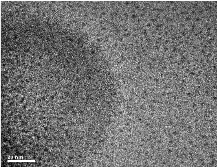 | ||
| Fig. 2 HR-TEM image of PbSe NCs prepared at 50 °C for one minute (C-1) (scale bar in the image is 20 nm). | ||
The absorption spectra for all three samples are shown in Fig. 3a and the photoluminescence (PL) spectra are shown in Fig. 3b. The blue shifts are clearly present in the absorption and PL spectra with the decrease of nanocrystal size. The blue shift and the characteristic time of PL decay (discussed in detail later on) confirm that intensive PL emission peaks between 780 and 850 nm are excitonic transitions. The relatively large value of the Stokes shift was calculated for PbSe NC samples as shown in the inset in Fig. 3a. There are many factors influencing the Stokes shift. However, its large value observed for our NCs most likely arises from the many energy levels characterized by different oscillation strengths as has already been shown for the near-edge energy spectrum of 3 nm PbSe NCs.31 Thus, the contribution of particular energy levels to absorption and emission spectra can be different giving rise to the large values of the Stokes shift. We also note that the observed increase in Stokes shifts for smaller NCs is in good agreement with the experimental values in the literature.13,32
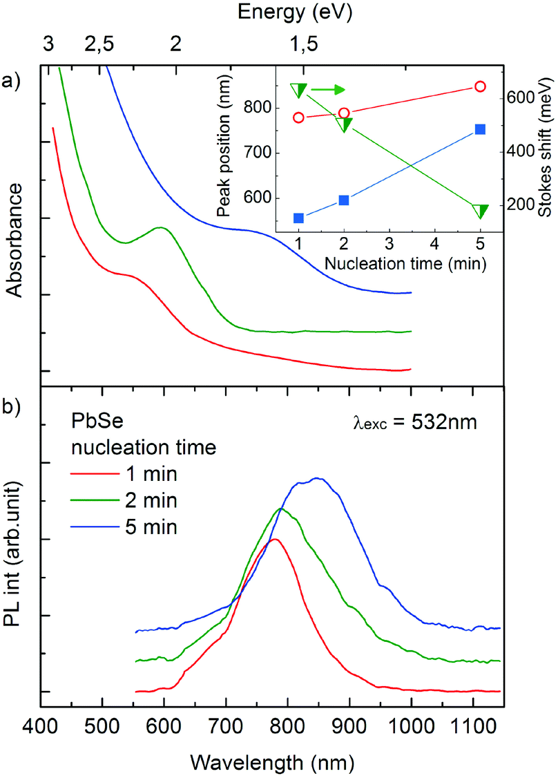 | ||
| Fig. 3 Absorption (a) and PL (b) spectra. The inset shows the absorption (blue rectangles) and emission (red open circles) band position, as well as the Stokes shift (half open green triangles) in a function of nucleation time. | ||
The PL efficiency is strictly related to the crystal quality of the samples and can be significantly reduced by e.g. crystal defects and surface states due to weak surface passivation by ligands, which can induce non-radiative exciton recombination. One more type of PL quenching mechanism in NCs can also be observed.
We investigated the photocharging of NC assembly by time traces of PL intensity variation when NC solution is static and stirred. We assumed that stirring is efficient enough and that the illuminated NC ensemble contains only neutral excitons and the charged NCs are outside the excitation volume.
Fig. 4 shows the time traces of C-1, C-2, and C-5 samples, when NC suspension was stirred or static (non-stirred). The PL intensity seems to be stable for every sample in all time ranges. When stirring is stopped, the accumulation of charged NCs in the excitation volume causes the PL intensity to decrease. In order to characterize the samples we used an F parameter determined as a ratio of PL intensity drop and its value when the solution is stirred (Fig. 4b). For all investigated samples the F parameter was relatively high, compared to the literature33 and a maximum value up to 42% was obtained for the C-2 sample. This is the sample for which the highest homogeneity among investigated samples was determined from broadening of an absorption spectrum. The unusually high F parameter determined for our small size PbSe NCs can find justification in the observation of the Klimov group, which associated PbSe and PbS NC photocharging with carrier (an electron or a hole) excitation into the 1P state.33 Moreover, Nootz et al. suggested that in smaller size particles, the strength of nominally forbidden transitions (e.g. 1S1P) increases due to an increase in the structural asymmetry.34 As a result, the probability of excitation to the 1P state via a 1S1P transition should increase with decreasing NC size. Thus, the likelihood of photocharging may increase for smaller sized NCs.
 | ||
| Fig. 4 Time traces of the PL intensity recorded for stirred (PLstir) and static (PLstat) NC solutions. The decrease of PL intensity means that charging of NC takes place. F parameter says how many NC are charging. | ||
We measured PL decays for C-1, C-2 and C-5 samples and the results are presented in Fig. 5 and a difference in PL dynamics of charged and uncharged NCs can be observed. As previously, the excitation wavelength was 532 nm and the PL decays were measured for static and stirred NC solutions. In general, NC solution is a complex ensemble of non-perfect NCs and, moreover, some of them are charged under the experimental conditions. Thus, it is expected that the PL decays are of complex nature and an appropriate function should be used to fit the experimental PL decays. In these experiments we used a stretched exponential function, which takes into account a distribution of relaxation time.35 In Fig. 5b, the fitting parameters are summarized. The expected value of the effective PL decay times 〈τ〉, which were calculated based on the fitting parameters, decreased for samples synthesized for longer than 1 minute. Moreover, the value of 〈τ〉 does not depend on the static–stirring conditions. On the other hand, the β parameter describes how much non-exponential a PL decay process is. β does not vary significantly from sample to sample, but increases clearly when the NC solution is stirred.
 | ||
| Fig. 5 PL decays recorded for static (filled blue dots) and stirred (open green dots) NC solutions (a); expected value of the effective relaxation time 〈τ〉 and β parameters obtained from stretched exponential function fitting (solid line and filled dots for static, dotted line and open dots for stirred case) (b). Uncertainties of fitting parameters are smaller than dots on the graph. | ||
The interpretation of the observed changes in PL decay times of NC solution upon static–stirring transitions is not as clear as previously proposed for a single NC experiment. However, based on the fact that the expected value of the effective PL decay times 〈τ〉 is unaffected by stirring, we propose that the observed NC charging is due to the electron-accepting surface sites. These sites intercept ‘hot’ electrons, before they relax into emitting core states.35–37 Thus, the small size of NCs and the related high surface-to-volume ratio may be an origin of the reported high efficiency charging.
Photovoltaic properties of PbSe NCs
The light capturing efficiency of as-prepared ultra-small PbSe NCs was investigated by fabricating an ETA solar cell. The details of the fabrication process of the electrode and sensitization of PbSe nanocrystals are described in the Experimental section.The incident photon to energy conversion efficiency (IPCE) spectra were measured by illuminating the cell through the composite layer. The ZnO–SnO2 layer provides the route for electron transport. The comparatively low IPCE in the UV region (300–400 nm) may be partly due to the strong light absorption of the FTO layer. The IPCE of devices consisting of electrodes D-1 and D-2 was found to be ∼7.3 and ∼8% respectively (Fig. S4, ESI†). The IPCE of the ETA cell shows appreciable photon to electron conversion efficiencies in the visible region, with a maximum efficiency of ∼8% in the 500–600 nm range.
Fig. 6a illustrates the internal structure of the constructed ETA device while Fig. 6b depicts interfacial charge transfer processes occurring at a typical metal oxide/PbSe/PEDOT:PSS (hole transporting material) interface.28,29 Under the impact of photons from light, PbSe NCs produce electrons and holes (exciton) as shown in step 1. The excited electron is then injected into the conduction band of the sensitizer (step 2). Step 3 represents the hole transport material. Efficient operation of the ETA device requires a high yield of interfacial charge separation and the minimization of recombination losses. Consequently, bulk PbSe is not suitable for such devices due to the lower thermodynamic driving force (ΔG) for electron injection and the regeneration processes.28
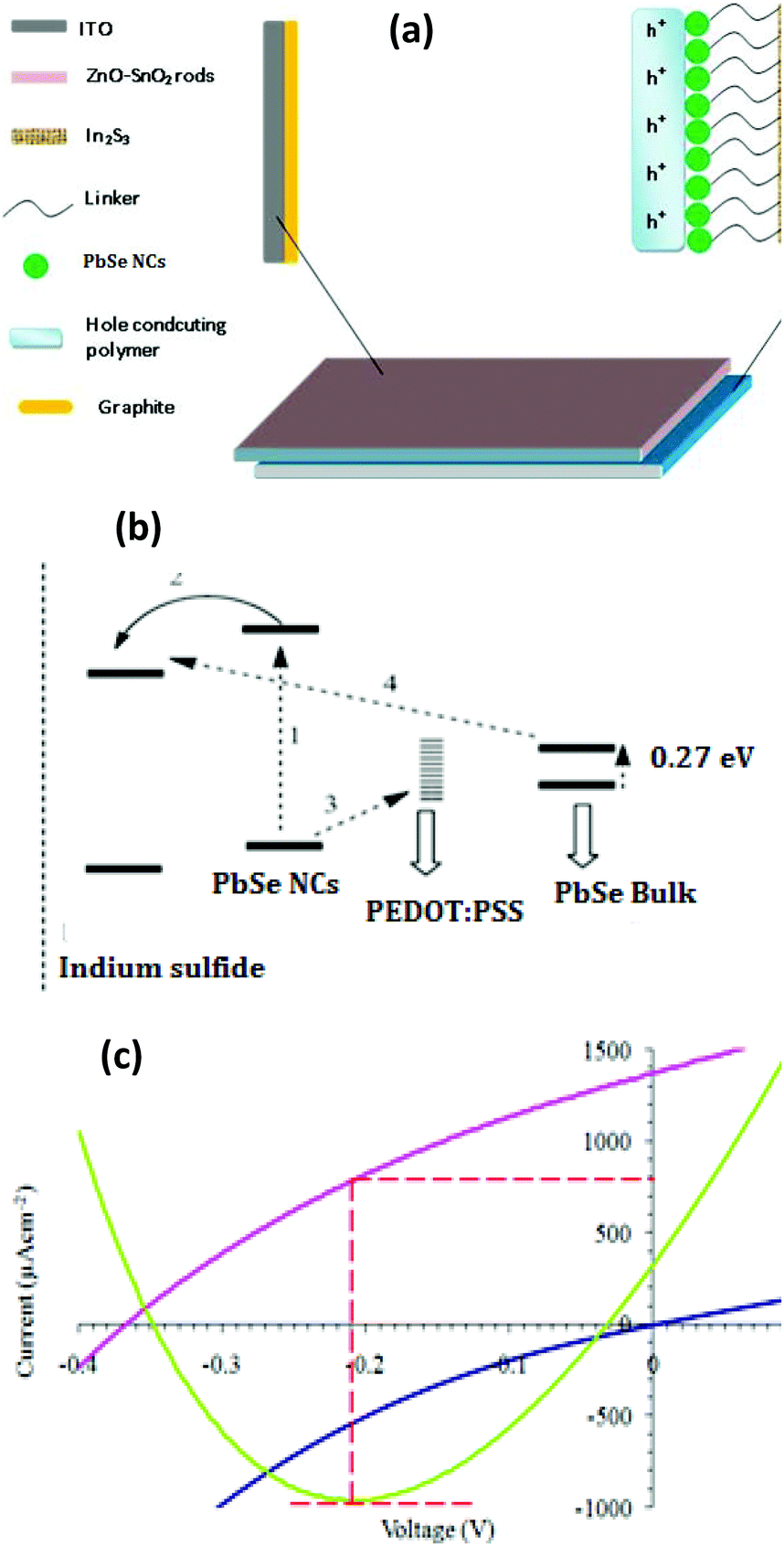 | ||
| Fig. 6 (a) Schematic diagram of the as-constructed ETA cell. (b) Simplified illustration of the chemical reactions at the interface of the ETA device, following photoexcitation from PbSe NCs.28 (c) Current–voltage measured characteristics of the ETA solar device containing the electrode D-2. | ||
The schematic energy diagram shown in Fig. 6c proposed for the cell device suggests that only quantized PbSe NCs are able to effectively inject electrons into the conduction band of In2S3 leading to the highest photon to electron conversion efficiency of 7–8%.28
The cells displayed a short circuit current density (Jsc) of 650 μA cm−2 and a Voc 0.33, a fill factor 0.33 and an overall efficiency of 0.07%. However, the cell containing the electrode (D-2) showed enhanced Jsc and Voc (Fig. 6c). The short circuit current density (Jsc) was 1379 μA cm−2 and Voc was 0.36. The calculated fill factor (FF) in this case was 0.33 and the overall efficiency was 0.17%. The higher current density and efficiency of the cell containing the electrode (D-2) showed that ligand exchanged PbSe NCs efficiently attached themselves on the surface of the electrode. Therefore, large IPCE values were observed. The direct sensitization method of PbSe NCs on the surface did not completely replace the long chain insulating capping molecule which affects the Jsc and Voc as well.
Conclusion
Ultra-small PbSe NCs were prepared in a one-pot using a greener route method. The optical studies of the as-prepared PbSe NCs showed that these NCs have a high potential in photovoltaic applications. The ETA solar device fabricated using these NCs showed promising photovoltaic activity. Further studies are in progress to evaluate and optimize the configuration of a device for higher conversion of sunlight and also to study the effect of PbSe nanoparticles on photovoltaic characteristics.Acknowledgements
The authors greatly acknowledge and thank the Dr Upul Wijayantha research group, Department of Chemistry, Loughborough University, Loughborough for providing lab facilities to do photoelectrochemical measurements. J.A. thanks the COMSATS Institute of Information Technology (CIIT), Islamabad for funding the project, no. 16-61/CRGP/CIIT/IBD/12/943 and also acknowledges the financial assistance from higher education commission (HEC). M.B. would like to acknowledge The Iuventus Plus program (no. IP2011 001271) and the Foundation for Polish Science (FNP) “Start” program for financial support. N.R. acknowledges the National Research Foundation (South Africa) for funding.References
- G. I. Koleilat, L. Levina, H. Shukla, S. H. Myrskog, S. Hinds, A. G. Pattantyus-Abraham and E. H. Sargent, ACS Nano, 2008, 2, 833–840 CrossRef CAS PubMed.
- T. Otto, C. Miller, J. Tolentino, Y. Liu, M. Law and D. Yu, Nano Lett., 2013, 13, 3463–3469 CrossRef CAS PubMed.
- D. D. Wanger, R. E. Correa, E. A. Dauler and M. G. Bawendi, Nano Lett., 2013, 13, 5907–5912 CrossRef CAS PubMed.
- M. H. Zarghami, Y. Liu, M. Gibbs, E. Gebremichael, C. Webster and M. Law, ACS Nano, 2010, 4, 2475–2485 CrossRef CAS PubMed.
- N. Zhao, T. P. Osedach, L.-Y. Chang, S. M. Geyer, D. Wanger, M. T. Binda, A. C. Arango, M. G. Bawendi and V. Bulovic, ACS Nano, 2010, 4, 3743–3752 CrossRef CAS PubMed.
- M. C. Beard, K. P. Knutsen, P. Yu, J. M. Luther, Q. Song, W. K. Metzger, R. J. Ellingson and A. J. Nozik, Nano Lett., 2007, 7, 2506–2512 CrossRef CAS PubMed.
- J. M. Luther, M. C. Beard, Q. Song, M. Law, R. J. Ellingson and A. J. Nozik, Nano Lett., 2007, 7, 1779–1784 CrossRef CAS PubMed.
- J. E. Murphy, M. C. Beard, A. G. Norman, S. P. Ahrenkiel, J. C. Johnson, P. Yu, O. I. Mićić, R. J. Ellingson and A. J. Nozik, J. Am. Chem. Soc., 2006, 128, 3241–3247 CrossRef CAS PubMed.
- J. S. Steckel, S. Coe-Sullivan, V. Bulović and M. G. Bawendi, Adv. Mater., 2003, 15, 1862–1866 CrossRef CAS.
- I. Kang and F. W. Wise, J. Opt. Soc. Am. B, 1997, 14, 1632–1646 CrossRef CAS.
- W.-k. Koh, A. C. Bartnik, F. W. Wise and C. B. Murray, J. Am. Chem. Soc., 2010, 132, 3909–3913 CrossRef CAS PubMed.
- C. B. Murray, S. Sun, W. Gaschler, H. Doyle, T. A. Betley and C. R. Kagan, IBM J. Res. Dev., 2001, 45, 47–56 CrossRef CAS.
- Q. Dai, Y. Wang, X. Li, Y. Zhang, D. J. Pellegrino, M. Zhao, B. Zou, J. Seo, Y. Wang and W. W. Yu, ACS Nano, 2009, 3, 1518–1524 CrossRef CAS PubMed.
- W. W. Yu, J. C. Falkner, C. T. Yavuz and V. L. Colvin, Chem. Commun., 2004, 2306–2307 RSC.
- J. Joo, J. M. Pietryga, J. A. McGuire, S.-H. Jeon, D. J. Williams, H.-L. Wang and V. I. Klimov, J. Am. Chem. Soc., 2009, 131, 10620–10628 CrossRef CAS PubMed.
- J. Tang, L. Brzozowski, D. A. R. Barkhouse, X. Wang, R. Debnath, R. Wolowiec, E. Palmiano, L. Levina, A. G. Pattantyus-Abraham, D. Jamakosmanovic and E. H. Sargent, ACS Nano, 2010, 4, 869–878 CrossRef CAS PubMed.
- A. G. Pattantyus-Abraham, I. J. Kramer, A. R. Barkhouse, X. Wang, G. Konstantatos, R. Debnath, L. Levina, I. Raabe, M. K. Nazeeruddin, M. Grätzel and E. H. Sargent, ACS Nano, 2010, 4, 3374–3380 CrossRef CAS PubMed.
- J. M. Luther, J. Gao, M. T. Lloyd, O. E. Semonin, M. C. Beard and A. J. Nozik, Adv. Mater., 2010, 22, 3704–3707 CrossRef CAS PubMed.
- J. A. McGuire, M. Sykora, J. Joo, J. M. Pietryga and V. I. Klimov, Nano Lett., 2010, 10, 2049–2057 CrossRef CAS PubMed.
- W.-k. Koh, Y. Yoon and C. B. Murray, Chem. Mater., 2011, 23, 1825–1829 CrossRef CAS.
- F. Wang, R. Tang, J. L. F. Kao, S. D. Dingman and W. E. Buhro, J. Am. Chem. Soc., 2009, 131, 4983–4994 CrossRef CAS PubMed.
- C. M. Evans, M. E. Evans and T. D. Krauss, J. Am. Chem. Soc., 2010, 132, 10973–10975 CrossRef CAS PubMed.
- J. Ouyang, C. Schuurmans, Y. Zhang, R. Nagelkerke, X. Wu, D. Kingston, Z. Y. Wang, D. Wilkinson, C. Li, D. M. Leek, Y. Tao and K. Yu, ACS Appl. Mater. Interfaces, 2011, 3, 553–565 CAS.
- W. Ma, S. L. Swisher, T. Ewers, J. Engel, V. E. Ferry, H. A. Atwater and A. P. Alivisatos, ACS Nano, 2011, 5, 8140–8147 CrossRef CAS PubMed.
- M. A. Hines and G. D. Scholes, Adv. Mater., 2003, 15, 1844–1849 CrossRef CAS.
- J. Akhtar, M. Afzaal, M. Banski, A. Podhorodecki, M. Syperek, J. Misiewicz, U. Bangert, S. J. O. Hardman, D. M. Graham, W. R. Flavell, D. J. Binks, S. Gardonio and P. O'Brien, J. Am. Chem. Soc., 2011, 133, 5602–5609 CrossRef CAS PubMed.
- J. Akhtar, M. A. Malik, P. O'Brien and M. Helliwell, J. Mater. Chem., 2010, 20, 6116–6124 RSC.
- R. Dharmadasa, K. G. U. Wijayantha and A. A. Tahir, J. Electroanal. Chem., 2010, 646, 124–132 CrossRef CAS PubMed.
- B. O'Regan and M. Gratzel, Nature, 1991, 353, 737–740 CrossRef.
- Q. Dai, Y. Wang, X. Li, Y. Zhang, D. J. Pellegrino, M. Zhao, B. Zou, J. Seo, Y. Wang and W. W. Yu, ACS Nano, 2009, 3, 1518–1524 CrossRef CAS PubMed.
- R. Leitsmann and F. Bechstedt, ACS Nano, 2009, 3, 3505–3512 CrossRef CAS PubMed.
- E. Lifshitz, M. Brumer, A. Kigel, A. Sashchiuk, M. Bashouti, M. Sirota, E. Galun, Z. Burshtein, A. Q. Le Quang, I. Ledoux-Rak and J. Zyss, J. Phys. Chem. B, 2006, 110, 25356–25365 CrossRef CAS PubMed.
- L. A. Padilha, I. Robel, D. C. Lee, P. Nagpal, J. M. Pietryga and V. I. Klimov, ACS Nano, 2011, 5, 5045–5055 CrossRef CAS PubMed.
- G. Nootz, L. A. Padilha, P. D. Olszak, S. Webster, D. J. Hagan, E. W. Van Stryland, L. Levina, V. Sukhovatkin, L. Brzozowski and E. H. Sargent, Nano Lett., 2010, 10, 3577–3582 CrossRef CAS PubMed.
- C. Galland, Y. Ghosh, A. Steinbrück, J. A. Hollingsworth, H. Htoon and V. I. Klimov, Nat. Commun., 2012, 3, 908 CrossRef PubMed.
- L. W. Golacki, A. Podhorodecki, J. Misiewicz and N. V. Gaponaneko, Opt. Express, 2010, 18, 22004 CrossRef PubMed.
- K. Weron, A. Jurlewicz, M. Magdziarz, A. Weron and J. Trzmiel, Phys. Rev. E: Stat. Phys., Plasmas, Fluids, Relat. Interdiscip. Top., 2010, 81, 041123 CrossRef.
Footnote |
| † Electronic supplementary information (ESI) available. See DOI: 10.1039/c4dt01941e |
| This journal is © The Royal Society of Chemistry 2014 |