 Open Access Article
 This Open Access Article is licensed under a
 Creative Commons Attribution 3.0 Unported Licence
Heteroatom-doped graphene materials: syntheses, properties and applications
Xuewan
Wang
a,
Gengzhi
Sun
a,
Parimal
Routh
a,
Dong-Hwan
Kim
a,
Wei
Huang
b and
Peng
Chen
*a
aSchool of Chemical and Biomedical Engineering, Nanyang Technological University, 70 Nanyang Drive, 637457, Singapore. E-mail: ChenPeng@ntu.edu.sg
bSingapore-Jiangsu Joint Research Center for Organic/Bio-Electronics and Information Displays & Institute of Advanced Materials (IAM), Nanjing Tech University, 30 South Puzhu Road, Nanjing, 211816, China
First published on 23rd June 2014
Abstract
Heteroatom doping can endow graphene with various new or improved electromagnetic, physicochemical, optical, and structural properties. This greatly extends the arsenal of graphene materials and their potential for a spectrum of applications. Considering the latest developments, we comprehensively and critically discuss the syntheses, properties and emerging applications of the growing family of heteroatom-doped graphene materials. The advantages, disadvantages, and preferential doping features of current synthesis approaches are compared, aiming to provide clues for developing new and controllable synthetic routes. We emphasize the distinct properties resulting from various dopants, different doping levels and configurations, and synergistic effects from co-dopants, hoping to assist a better understanding of doped graphene materials. The mechanisms underlying their advantageous uses for energy storage, energy conversion, sensing, and gas storage are highlighted, aiming to stimulate more competent applications.
 Xuewan Wang | Xuewan Wang received his BS from Yantai University (China) in 2008 and MS from Zhejiang University (China) in 2011. He is currently a 3rd year PhD student in Prof. Peng Chen's group in Nanyang Technological University (Singapore). His main research focus is on the synthesis of graphene materials and their applications for energy storage and conversion, and sensing. |
 Peng Chen | Peng Chen is currently an Associate Professor in the School of Chemical and Biomedical Engineering at Nanyang Technological University (Singapore). He completed his PhD in the University of Missouri (Columbia) in 2002, followed by a period of postdoctoral research at Harvard University. His current research focuses on nanomaterials (particularly graphene), biosensors, and bionanotechnology, which has resulted in >120 publications. |
1 Introduction
In the past decade, we have witnessed immense progress in graphene research since the first isolation of this “wonder material”. Graphene has been changing the landscape of many fields in science and technology, particularly condensed matter physics,1,2 electronics,3,4 energy storage and conversion,5–7 and biomedical research.8–10 Tremendous efforts are still ongoing to uncover the full potential of graphene and its derivatives.The fascinating properties of pristine graphene (single-atom-thick layer of sp2 bonded carbon atoms tightly packed into a 2D honeycomb lattice) are now largely understood and well-recognized through extensive research in the past years.11–13 Although the lack of intrinsic bandgap and catalytic abilities seems to greatly limit the practical applications of pristine graphene, the legend of this 2D material is going to continue owing to its structural transformability and highly tunable properties. As recently demonstrated, new properties and application opportunities arise when graphene transforms from its native 2D structure to 0D (graphene quantum dots),14–17 1D (graphene nanoribbons)18,19 or 3D (graphene foam) structures.20–22 In addition, the physicochemical and electronic properties of graphene can be drastically altered by molecular and atomic doping.
Tailoring graphene properties by interacting molecules, which either donate or withdraw free electrons, has been demonstrated in many studies and discussed in recent review articles.23–25 Herein, we focus the discussion on the doping of graphene with various heteroatoms (oxygen, boron, nitrogen, phosphor, sulfur, etc.), i.e., the graphitic carbon atoms are substituted or covalently bonded by foreign atoms. Although several review articles focusing on specific dopants or particular applications have been published,26–29 a more comprehensive and comparative review on this important and quickly evolving topic is necessary. In this article, the synthesis methods, properties and applications of graphene materials doped with various heteroatoms are reviewed extensively. We aim to cover the latest developments, underscore physical mechanisms, highlight unique application-specific advantages conferred by doping, and provide insightful comparison between doped and pristine graphene, different synthesis routes, different dopant atoms, and different doping configurations.
2 Synthesis methods
A large variety of methods have already been developed for the synthesis of graphene materials, from which various doping strategies could be derived. The current methods for heteroatom doping can be categorized into in situ approaches and post-treatment approaches. In situ approaches, which simultaneously achieve graphene synthesis and heteroatom doping, include chemical vapor deposition (CVD), ball milling, and bottom-up synthesis. Post-treatment methods include wet chemical methods, thermal annealing of graphene oxides (GO) with heteroatom precursors, plasma and arc-discharge approaches. In this section, these methods are discussed and compared in detail (Table 1).| Methods | Precursors | Doping | Advantages and limitations | Ref. |
|---|---|---|---|---|
| CVD | H3BO3 + polystyrene | 4.3 at% B | Simultaneous growth and doping of large graphene sheet; controllable doping; complex process and high operating temperature; sometimes hazardous precursors and waste gases are produced; high cost and low yield. | 31 |
| Phenylboronic acid | 1.5 at% B | 36 | ||
| CH4 + H3NBH3 | 10–90 at% BN | 33 | ||
| CH4 + NH3 | 8.9 at% N | 42 | ||
| Sulfur in hexane | <0.6 at% S | 44 | ||
| Iodine + camphor | 3.1 at% I | 46 | ||
| Pyrimidine + thiophene | ≤5.7 N, 2.0 S at% | 45 | ||
| Ball milling | Pristine graphite (PG) + N2 | 14.8 wt% N | Simple and scalable process; doping only at edges; difficult to control the doping process. | 49 |
| PG + sulfur powder | 4.94 at% S | 53 | ||
| PG + Cl2/Br2 | 5.85 Cl/2.78 Br at% | 51 | ||
| Bottom-up synthesis | CCl4 + K + BBr3 | 2.56 at% B | Scalable solution-based reaction under mild conditions; unavoidable high oxygen content. | 54 |
| Li3N + CCl4 | 4.5–16.4 at% N | 55 | ||
| Pentachloropyridine + K | 3.0 at% N | 56 | ||
| Thermal annealing | GO + BCl3 | 0.88 at% B | Wide choices of dopant precursors (gases, liquids, or solids); controllable doping; high temperature required, but helpful to recover sp2 carbon network. | 59 |
| GO + NH3 | 8 at% N | 63 | ||
| GO + melamine/PANI/PPy | 2–18 at% N | 70 and 71 | ||
| GO + ionic liquid | 22.1 N/1.16 P at% | 75 and 76 | ||
| GO + H2S | 1.2–1.7 at% S | 77 | ||
| GO + DDS + DDSe | 0.19 S, 0.05 Se at% | 80 | ||
| Graphite oxide + Cl2/Br2 | 5.9 Cl/9.93 Br at% | 84 | ||
| Wet chemical method | GO + hydrazine | 4.5 at% N | Amenable to low-cost, low-temperature, solution-based mass production; easily achieve doping and decoration (e.g., with various nanoparticles) simultaneously; conveniently form 3D gel structure. | 86 |
| GO + urea | 10.13 at% N | 91 | ||
| GO + NH4SCN | 18.4 N, 12.3 S at% | 95 | ||
| GO + HF/HI | 1.38 F/4.33 I wt% | 96 | ||
| PG + Cl2/Br2 | 21 Cl/ 4 Br at% | 99 | ||
| Plasma | GO + N2 | 2.51 at% N | Short reaction time and low power consumption; low yield. | 108 |
| CVD graphene + Cl2 | 45.3 at% Cl | 112 | ||
| Photo-chemistry | CVD graphene + Cl2, xenon lamp irradiation | 8 at% Cl | Short reaction time and low power consumption; low yield. | 113 |
| Arc-discharge | PG + NH3 | 1 at% N | Mass-production; high voltage or current required; low doping level; mainly multilayer graphene. | 114 |
| PG + B/B2H6 | 3.1 at% B | 115 | ||
| PG + graphite fluoride | 10 wt% F | 116 | ||
2.1 In situ doping
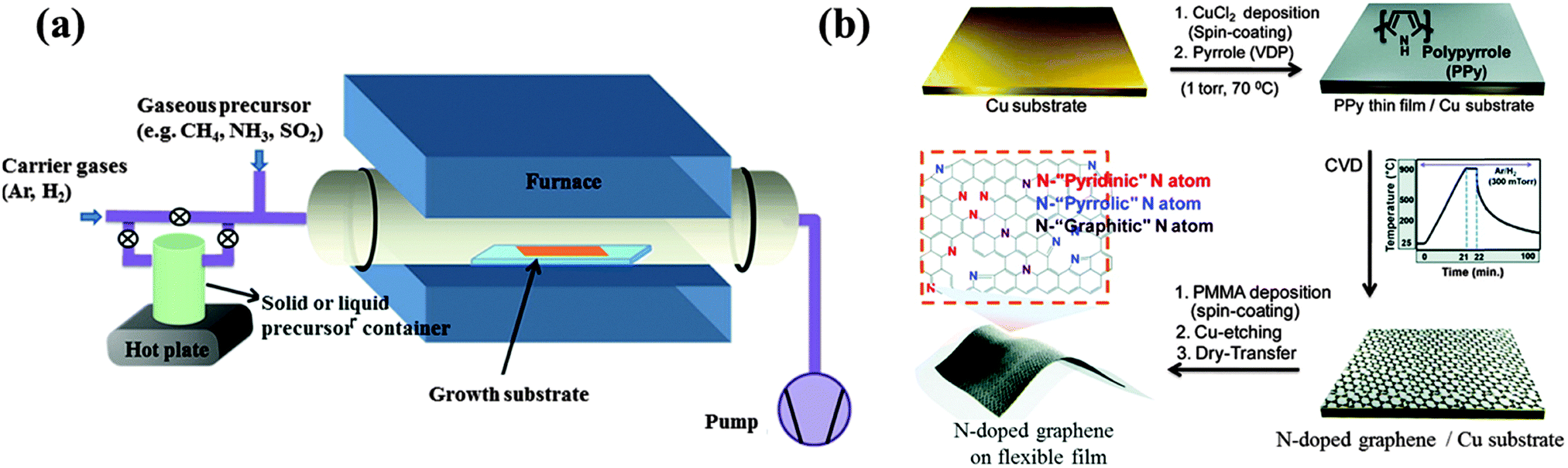 | ||
| Fig. 1 (a) Experimental setup commonly used for CVD graphene doping. Adapted with permission from ref. 30. Copyright (2013) American Chemical Society. (b) N-doped graphene derived from polypyrrole. Adapted with permission from ref. 39. Copyright (2012) American Chemical Society. | ||
Because boron (B) and nitrogen (N) have similar sizes and valence electron numbers as carbon (C), it is relatively easier to incorporate them into graphene. For example, B-doped graphene with a doping level of 4.3 at% (atomic percentage) was grown on a copper (Cu) foil at 1000 °C under the protection of H2/Ar atmosphere, using boric acid and polystyrene as the B and C sources, respectively.31 These solid-phase feedstocks are sublimated upstream and transported by the carrier gases toward the growth substrate (Fig. 1a). B-doping was also realized using ethanol as the carbon source and boron powder as the B-precursor.32 There are two bonding configurations of B atoms observed in CVD graphene lattice: “boron silane” boron (BC4) and graphitic boron (BC3). In contrast to the more commonly occurring BC3 bonding (B replacing C in the hexagonal carbon lattice), BC4 configuration is obtained due to the excess defects or edge sites. Dual B,N doped graphene was reported by Ajayan et al, using methane and ammonia borane (NH3–BH3) as the carbon and B,N sources, respectively.33 The doping level can be tuned by adjusting the reaction parameters. At high doping levels, the resultant large-area B,N co-doped graphene contains B–N hybridized domains (with B/N ratio, ∼1), as evidenced by the X-ray photoelectron spectroscopy (XPS) analyses. The incorporation of small BN domains (B/N ratio, 0.3–0.5) was also reported by Bepete et al., employing boric acid powder and N2 as the precursors.34 Using nickel foam as the growth template, B, N, or (B,N)-doped 3D graphene was also reported, which, when compared with its 2D counterparts, offers a larger active surface area.35
In comparison with the use of multiprecursors, a single precursor, containing both C and alien atom is believed to be more convenient and controllable. For instance, homogeneous B-doping on a graphene monolayer was produced using phenylboronic acid as the sole precursor, without significantly compromising the transmittance and conductivity of the graphene film.36 Pyridinic and pyrrolic N-doped graphene was synthesized using acetonitrile as the only precursor,37 while pyridinic N-doped graphene was CVD-grown, using pyridine as the sole source.38
Heteroatom-containing polymers (sometimes embedded in the polymeric carrier matrix) can be directly vapor-deposited or spin-coated atop the metal catalyst for graphene growth and in situ doping. Such processes are safer without the use of high-temperature gases and can achieve patterned doping. In the work of Kwon et al., pyrrole monomers vapored on a Cu substrate were polymerized by the presence of Cu2+ ions, followed by CVD growth (Fig. 1b).39 The obtained N-doped few-layered graphene contains 3.14 at% N with dominating pyrrolic N probably inherited from the polypyrrole precursor. Sun et al. directly spin-coated the mixture of N-rich melamine and PMMA on a Cu substrate for the growth of N-doped graphene at 1000 °C under atmospheric pressure, reaching a doping level of 2–3.5 at%.40 It is known that melamine can evolve into two-dimensional graphene-like graphitic carbon nitride (g-C3N4).41 Although the configuration of N-doping is mainly graphitic, the mobility of the obtained N-graphene is poor (<10 cm2 V−1 s−1).40
A gaseous precursor is the most commonly used, for which the doping level can be readily controlled by the flow rates (and thus, the percentage ratio between the gaseous reactants). Further, Wei et al. firstly reported the experimental synthesis of N-doped graphene with CH4 and NH3 as the C and N sources, respectively.42 The growth temperature and the ratio between CH4 and NH3 exert a considerable influence on the bonding structure of doped nitrogen. The few-layered N-graphene synthesized at 800 °C enjoys a high N level of 8.9 at%, among which graphitic N is the dominant species (as compared to the co-existing pyridinic and pyrrolic N),42 whereas N-doped graphene synthesized at 1000 °C exhibits dominating pyridinic N and a small fraction of pyrrolic N.43
Fluorine gas (F2) and F-containing compounds are toxic and too reactive at high temperatures. Therefore, to the best of our knowledge, there is still no report on the synthesis of F-doped graphene using the CVD method. Further, it is energetically unfavorable to incorporate large-sized atoms (e.g., silicon, Si; phosphorus, P; sulfur, S; chlorine, Cl; iodine, I) into graphene. Gao et al. demonstrated the CVD growth of S-doped graphene on a Cu substrate using sulfur powder dissolved in hexane as the precursor.44 However, the S-doping level is extremely low (<0.6 at%), likely in the form of –C–S–C– and preferably at the defect sites due to the lowered binding energy. Xu et al. synthesized N, S co-doped graphene at a relatively low temperature of 700 °C using pyrimidine (N, C source) and thiophene (S, C source) as the precursors.45 N and S atoms in the co-doped graphene are uniformly distributed with the doping levels of 3.7 to 5.7 at% and 0.7 to 2.0 at%, respectively. Apart from the –C–S–C– bonding configuration, –C–SOx–C– is also speculated to exist. I-doped graphene was also made using the CVD method, where an iodine and camphor mixture was evaporated and pyrolyzed on a nickel substrate at 800 °C for 3 min.46 All the I atoms (3.1 at%) are doped via ionic bonding in aggregated forms (e.g., I3− and I5−).
By ball-milling graphite under N2 atmosphere over 48 h, Jeon et al. successfully fixed uncleaved N2 at the broken edges of graphene nanoplates with a high nitrogen content of 14.84 wt% (weight percentage) (Fig. 2a).49 They proposed that aromatic 5-membered pyrazole and 6-membered pyridazine rings are energy-favorably formed at zigzag and armchair edges, respectively (Fig. 2b and c). It is more likely to form zigzag edges due to the larger density of states near the Fermi level than that of the armchair edges.50 However, the stability of the 5N ring at the zigzag edges is inferior to the 6N ring at the armchair edges. In addition, the entropy gain from the grain size reduction and enthalpy increase from the edge functionalization facilitate the dispersion of graphene nanoplates in various polar solvents (e.g. water, methanol, isopropyl alcohol, DMF and NMP).51,52 This is desirable for further solution-based processes.
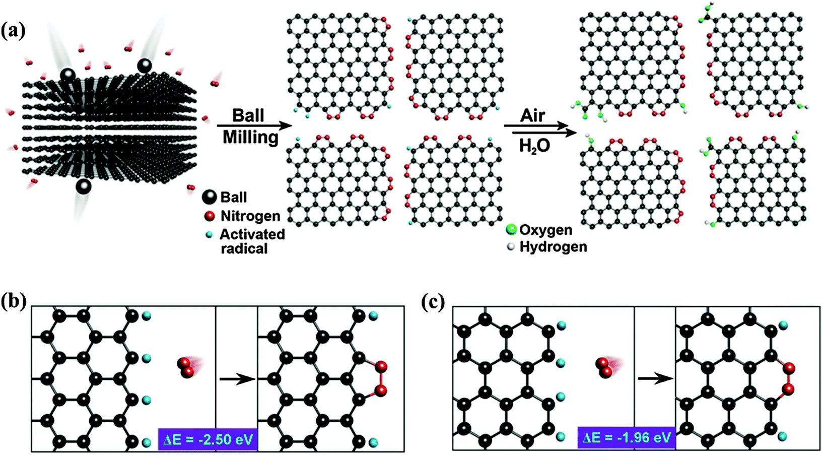 | ||
| Fig. 2 (a) A schematic representation of the physical cracking of graphite flakes in a ball-mill crusher in the presence of nitrogen and subsequent exposure to air moisture to produce N-doped graphene nanoplates. (b and c) The formation of a 5-membered pyrazole ring/6-membered pyridazine ring after the reaction between the active zigzag-edge carbon atoms/armchair-edge carbon atoms and nitrogen. Adapted with permission from ref. 49. Copyright (2013) Nature Publishing Group. | ||
Edge-sulfurized graphene nanoplatelets (SGnP) were also prepared by ball milling graphite in the presence of sulfur (S8) with uniformly-distributed sulfur elements at a level of 4.94 at%.53 Similarly, halogen atom-doped graphene nanoplates (ClGnP, BrGnP and IGnP) were synthesized in the presence of chlorine (Cl2), bromine (Br2) or iodine (I2), respectively.51 The decreasing doping levels (Cl at 5.89, Br at 2.78, and I at 0.95 at%) correlate with the decreasing chemical reactivity and increasing size of these elements. Analogous to ball milling, the N-doping of graphene was achieved by means of mechanically exfoliating graphene sheets by scotch-taping graphite in a nitrogen ambience.50 The freshly generated edges were immediately passivated by nitrogen. Because doping and defects were absent in the basal plane, high mobility of 5000 cm2 V−1 s−1 was measured.
![[double bond, length as m-dash]](https://www.rsc.org/images/entities/char_e001.gif) C– and –CB/N– into two-dimensional hexagonal carbon clusters; and (3) the growth of B/N-doped graphene from these clusters.54 Doping level can be readily controlled by the amount of heteroatom precursors for the WRC reaction. In comparison with CVD growth, it does not require transition metal catalysts, but high oxygen content will be unavoidably introduced.57 Peng et al. developed a different strategy to synthesize N-doped graphene-like sheets by annealing the mixture of PANI and melamine with the addition of Fe3+ ions at 900 °C.58 Fe is believed to catalyze the formation of a sheet structure.
C– and –CB/N– into two-dimensional hexagonal carbon clusters; and (3) the growth of B/N-doped graphene from these clusters.54 Doping level can be readily controlled by the amount of heteroatom precursors for the WRC reaction. In comparison with CVD growth, it does not require transition metal catalysts, but high oxygen content will be unavoidably introduced.57 Peng et al. developed a different strategy to synthesize N-doped graphene-like sheets by annealing the mixture of PANI and melamine with the addition of Fe3+ ions at 900 °C.58 Fe is believed to catalyze the formation of a sheet structure.
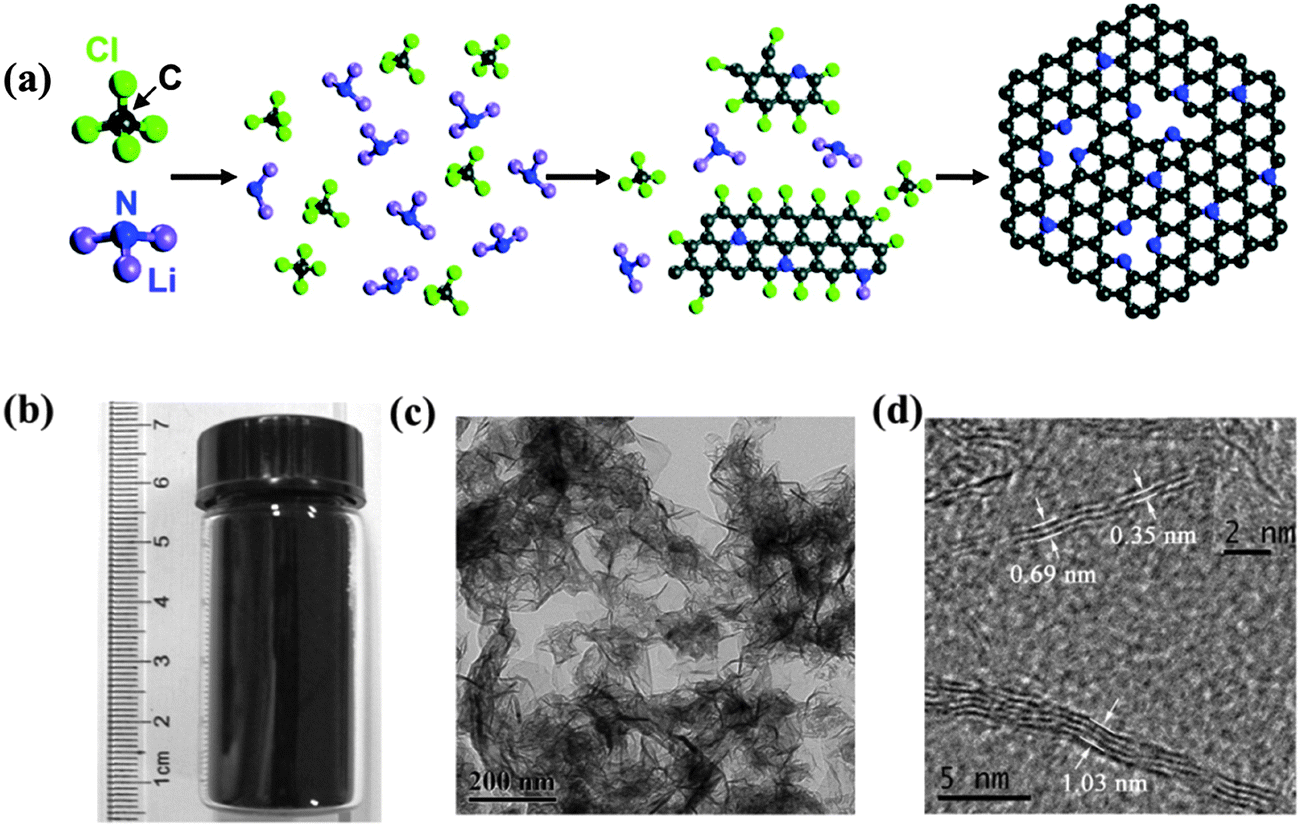 | ||
| Fig. 3 (a) Proposed mechanism for the solvothermal synthesis of N-doped graphene via the reaction of CCl4 and Li3N, where the gray balls represent C atoms; blue, N; green, Cl; and purple, Li. (b) Vial containing the prepared N-doped graphene sample. (c and d) TEM images of the synthesized N-doped graphene samples. Adapted with permission from ref. 55. Copyright (2011) American Chemical Society. | ||
2.2 Post-synthesis treatment
It is unambiguous that temperature is a key factor to determine the N-doping efficiency and bonding configuration. Annealing GO in low-pressure NH3/Ar atmosphere at different temperatures (from room temperature to 1100 °C), Li et al. found that N doping starts to occur at 300 °C and reaches the highest doping level of ∼5 at% at 500 °C.61 It is proposed that 500–600 °C is optimal for the overall stability of all the N species (amino, pyrrolic, pyridinic, and possibly graphitic N).62 Using such temperatures, an even higher N-doping level of ∼8 at% was reported.63,64 At lower temperatures (300–500 °C), N bonding configurations include amino, amide, and pyrrolic N. The amino groups dominate as amino free radicals from ammonia react with the oxygenated groups on GO. In contrast, pyridinic and pyrrolic N are dominant at a temperature of >800 °C.65–68 At a further elevated temperature, some pyridinic and pyrrolic N may be burnt by oxygen released from GO, leading to a decrease in the N content.66 It was reported that annealing at 1100 °C for a long time promotes the formation of graphitic N in the carbon lattice.67 These observations are consistent with the thermal stability of different N bonding configurations: graphitic N > pyridinic N > pyrrolic N. Moreover, Dai et al. demonstrated B,N co-doped graphene by simply thermally annealing GO in the presence of boric acid and NH3 at 1000 °C.69 They also suggested that the increase of annealing time facilitates the formation of BN clusters.
In addition to the annealing temperature, the doping efficiency and configuration also critically depend on the chosen precursor(s) (Fig. 4).70 In addition to NH3, melamine,71 polyaniline (PANI),70,72 polypyrrole (Ppy),70 cyanamide73 and dicyandiamide74 have also been employed. Using these precursors, the N-doping level ranges from 2 to 18 at%. Ionic liquids (IL), which contain N and/or P and whose surface tension and surface energy match well with that of graphene, can serve as excellent doping sources. Liu et al. annealed IL-electrolyzed graphene at a really low temperature of 400 °C and obtained a high N/C ratio of 22.1%.75 The N-bonding configuration is strongly dependent on the charge characteristics, viscosity, and other properties of the used ILs. For example, N-doped graphene synthesized using 1-butyl-3-methylimidazolium bromide ([Bmim]Br) shows the presence of pyrrolic N (major species) and graphitic N. In comparison, [Bmim][Ac] produced N-doped graphene shows dominant pyridinic N, while [Bmim]PF6 produced N-doping is equally contributed by pyridinic and pyrrolic forms. Furthermore, using [Bmim]PF6, but annealed at 1000 °C, P-doped graphene nanosheets (3–4 layers) were obtained.76 P-doping (1.16 at%) equally exists in the two bonding configurations: P–C and P–O.
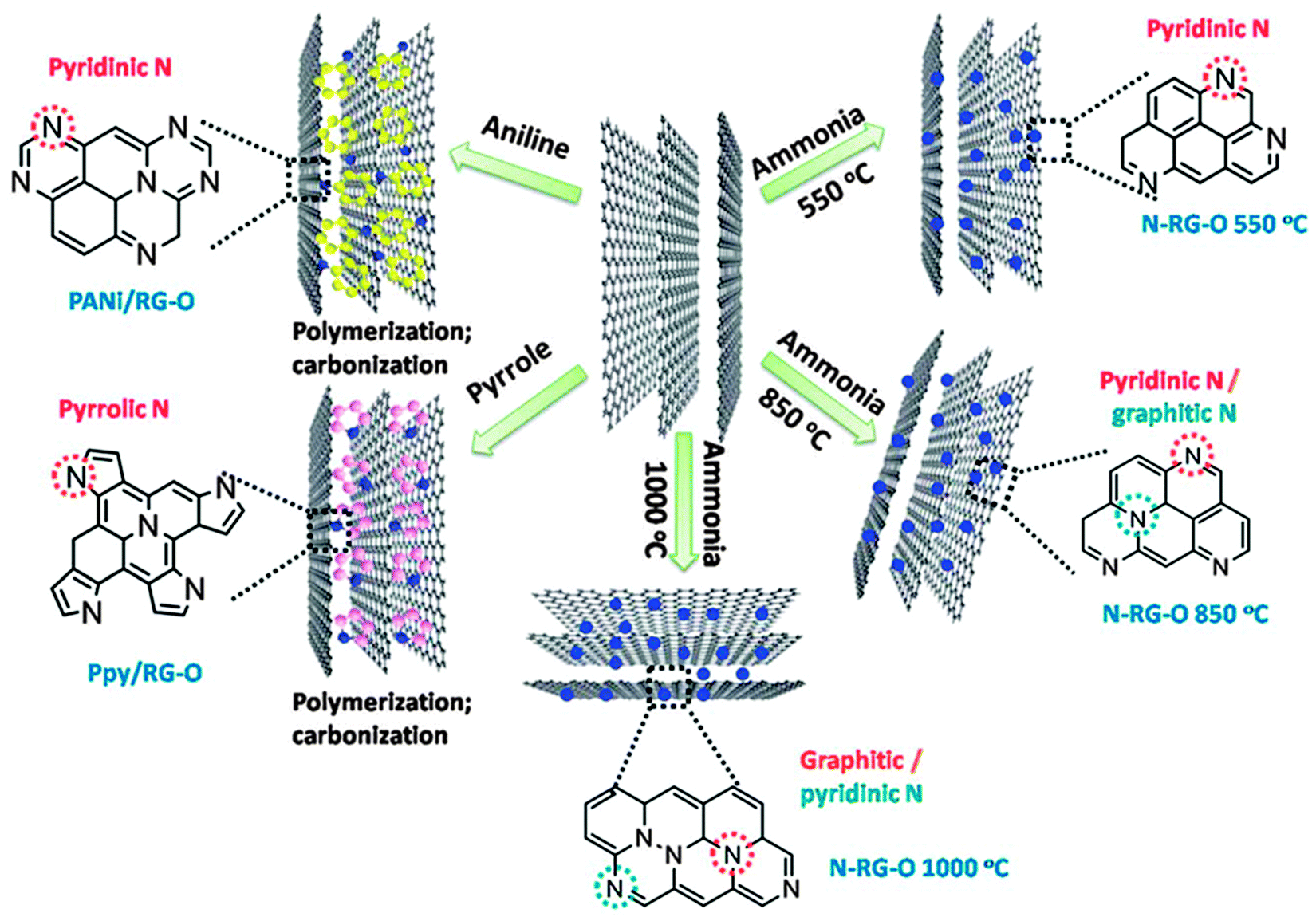 | ||
| Fig. 4 N-doping configuration depends on the precursor and temperature. Adapted with permission from ref. 70. Copyright (2012) Royal Society of Chemistry. | ||
To avoid aggregation during the annealing process and ensure free gas transport, Yang et al. used porous silica to confine GO sheets for N- or S-doping (Fig. 5).77 It was found that S-doping (1.2–1.7 at%) is less effective than N-doping, and S-doping occurring at the defect sites forms thiophene-like structure. The properties of GO (the abundance and composition of oxygenated groups) and chosen S-source (H2S, SO2 or CS2) exert great influences on doping.78 Seredych et al. doped S into graphene by heating rGO in H2S at 800 °C and 3 at% of S was introduced in the thiophenic groups and aromatic rings.79 The XPS analyses indicate that neutral S, –SH, –S2–O– and –SO– co-existed in the resultant materials. The solid precursors normally used for S/Se doping include diphenyldisulfide (DDS),80 phenyl disulfide (PDS),81 benzyl disulfide (BDS),82,83 and diphenyl diselenide (DDSe).80,82 Using BDS and melamine as the precursors, N,S co-doped graphene was produced with 2.0 at% of S and 4.5 at% of N.83
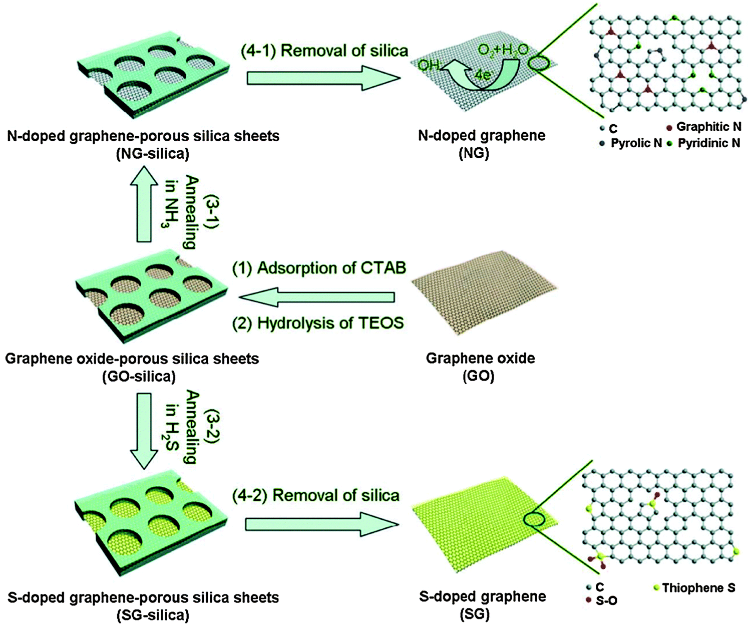 | ||
| Fig. 5 N- or S-doping on porous silica confined GO sheets by thermal annealing. Adapted with permission from ref. 77. Copyright (2012) Wiley Publishing Group. | ||
For halogen doping, Poh et al. successfully synthesized Cl-, Br- and I-doped graphene (with the doping levels of 5.9, 9.93 and 2.31 at%, respectively) by the thermal exfoliation/reduction of graphite oxide in halogen gas atmosphere.84 Considering the poor thermal stability of halogen-doped graphene, the doping process is conducted in a vacuum tight reactor with rapid temperature ramping/cooling rates. Similar to CVD processes, I-doping by this thermal process also relies on ionic bonding. The conductivity of Cl-graphene, Br-graphene and I-graphene increases in this order. On the other hand, their thermal stability decreases in the order in oxygen (but opposite in argon). Alternatively, Yao et al. prepared I-graphene by annealing GO and iodine in argon.85 With the increase of temperature from 500 to 1100 °C, the content of I decreases from 1.21 to 0.83 wt%.
 | ||
| Fig. 6 Schematic illustration of (a) nitrogen insertion routes in GO. (b) Routes for the formation of a hypothetical structure of graphitic N in GO. Adapted with permission from ref. 91. Copyright (2012) Royal Society of Chemistry. | ||
Su et al. used NH4SCN, which decomposes into highly reactive species (NH3, H2S, CS2) under hydrothermal condition, for N,S co-doping on GO.95 The homogeneous doping of S (12.3 at%) and N (18.4 at%) is achieved. N exists in pyridinic (64%) and graphitic (36%) forms, while S mainly dopes at the defect sites and edges in the form of –C–Sn–C– (n = 1 or 2, 55%), –CS– (35%) and other moieties (e.g. –SOn–, –SH). Garrido et al. modified GO with halogen atoms by hydrothermal approaches in HX solutions (X = F, Cl, Br or I), with doping levels of 4.38 (F), 2.28 (Cl), 5.36 (Br), and 4.33 (I) wt%.96
Halogen-doped graphene can also be obtained by the liquid-phase exfoliation (e.g., sonication) of graphite halide.97,98 However, the doping level cannot be tuned using such methods, and it is usually challenging to make a large amount of halogenated graphite except fluorinated graphite. Recently, Zheng et al. developed an interesting microwave-spark method to synthesize Cl- and Br-doped graphite in the presence of liquid chlorine and bromine, which could then be easily exfoliated into single-layered Cl-/Br-doped graphene sheets via sonication (Fig. 7).99 Under the luminous microwave-sparks, active graphite flakes generated by a short temperature shock can react with halogen precursors. Subsequent rapid temperature decrease quenches the reaction and prevents the thermal decomposition of the resultant materials. The obtained graphene sheets contain high percentages of covalently bonded Cl and Br (21 at% and 4 at%, respectively). Different from GO, the resulting doped-graphene is strongly hydrophobic and disperses well in organic solvents (Fig. 7).
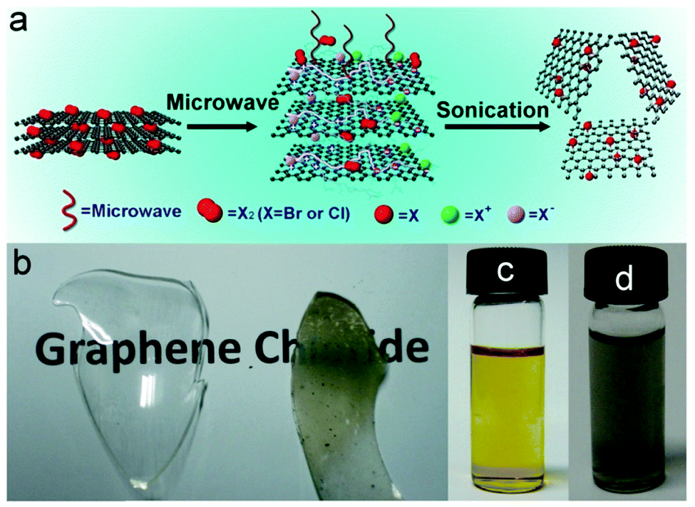 | ||
| Fig. 7 (a) Synthesis of Cl- or Br-doped single-layer graphene sheets using microwave-spark method. (b) Photographs of the graphite chloride coated on the inside surface of the flask. (c and d) Photographs of Cl- and Br-doped graphene dispersion in DMF, respectively. Adapted with permission from ref. 99. Copyright (2012) Nature Publishing Group. | ||
Using wet chemical methods, heteroatoms have also been doped on 3D graphene gels, having a large surface area and macroporous structure.94,95,100,101 For example, Wu et al. employed ammonia boron trifluoride (NH3BF3) for the co-doping of B and N.101 The simultaneous reduction and self-assembly of GO sheets under the hydrothermal condition in addition to the subsequent freeze-drying process cause the formation of B,N-doped rGO aerogel. Solution-based doping processes also permit the simultaneous decoration of various functional nanomaterials (e.g. metallic nanoparticles,102 metal oxide nanoparticles103–107). The doped heteroatoms facilitate the nucleation and anchoring of these nanoparticles.
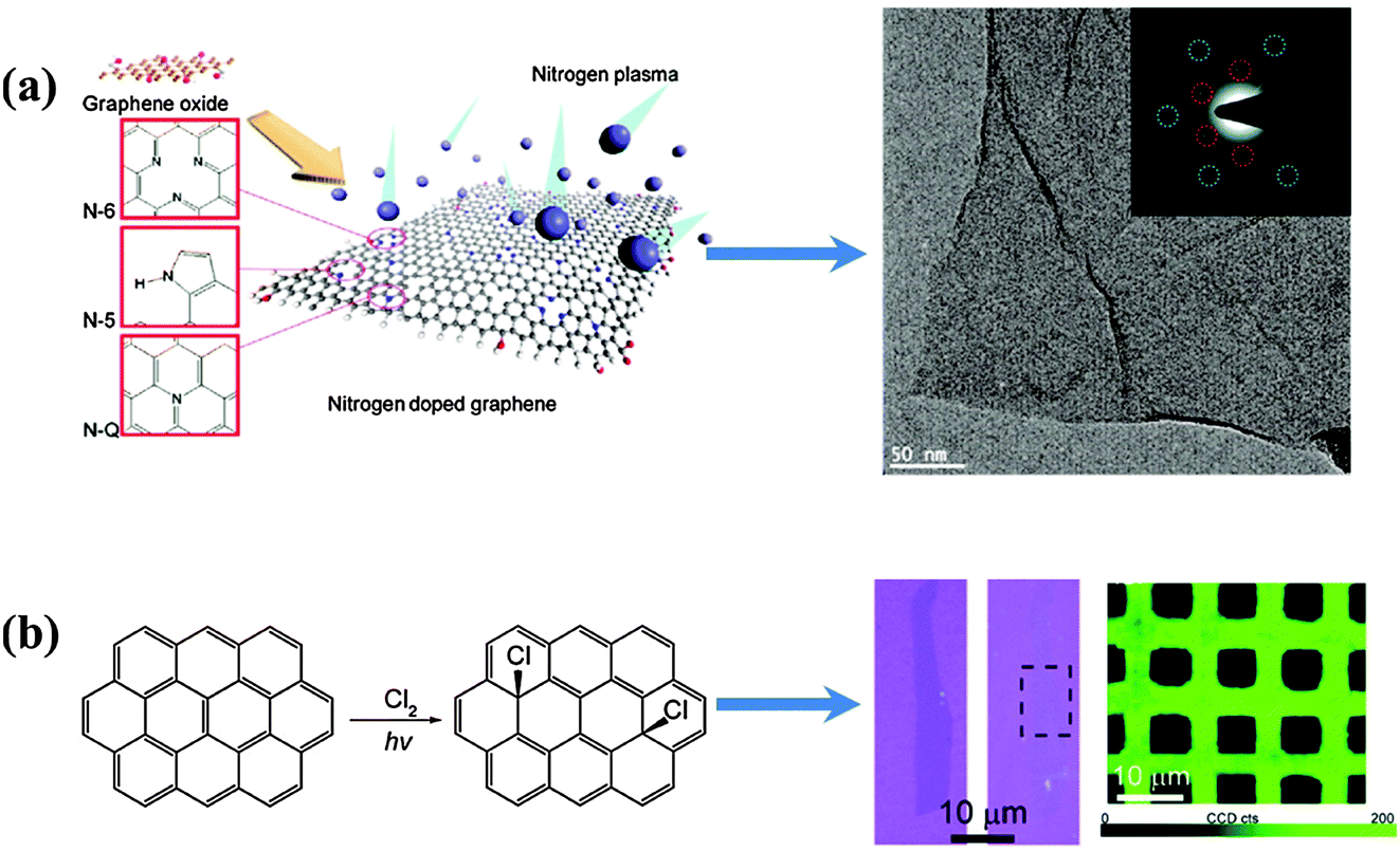 | ||
| Fig. 8 (a) Schematic illustration of nitrogen plasma doping process with possible N configurations (left side); a high-resolution TEM image (right side) and selected area electron diffraction (inset) of the N-doped graphene indicate that the intrinsic layered structure and original honeycomb-like atomic structure were preserved during the plasma process. Adapted with permission from ref. 108. Copyright (2011) American Chemical Society. (b) Scheme of the photochemical chlorination process (left); optical images of a single-layer graphene sheet before and after photochemical chlorination, respectively (right, blue color); D band mapping (λex = 514.5 nm) of CVD-grown graphene film after patterned photochlorination (right, green colour). Adapted with permission from ref. 113. Copyright (2011) American Chemical Society. | ||
However, the level of N-doping attainable by plasma treatment is generally less as compared to other doping methods. Plasma technique is particularly effective for halogen atom doping because halogen atoms are highly reactive. Wu et al. demonstrated plasma-assisted chlorine-doping on CVD graphene at a low power, without the generation of considerable defects.111 A Cl coverage of 8.5 at% and conductance enhancement due to the p-doping effect were observed. By tuning the plasma conditions (reaction time, dc bias, vacuum level, etc.), Zhang et al. achieved extremely high Cl-doping of 45.3 at% (close to C2Cl) on CVD graphene.112 The C/Cl ratio and bonding states (C–Cl interaction through ionic bonding, covalent bonding, and defect creation) are sensitive to the DC bias applied.
Li et al. developed a photochemical method for homogeneous and patternable Cl-doping on graphene (Fig. 8b).113 Under the xenon lamp radiation (maximum power density of 1.4 W cm−2), chlorine molecules split into highly reactive radicals, which, in turn, covalently conjugate to the basal carbon atoms of graphene. Homogeneous doping (∼8 at%) was verified by Raman mapping. Interestingly, doped-graphene becomes more transparent due to the widening of the graphene bandgap.
The arc-discharge approach is another technique to create reactive heteroatom radicals for graphene doping. Li et al. prepared N-doped multi-layered graphene sheets (1 at%) by DC arc-discharge using NH3 as the buffer gas.114 NH3 not only acts as a N precursor but also suppresses the formation of fullerenes by terminating the edge-sited dangling C bonds with the decomposed reactive hydrogen. In addition to NH3, H2 along with B2H6, boron-stuffed graphite and H2 along with pyridine have also been utilized as the heteroatom precursors in arc-discharge processes for the synthesis of B- and N-doped graphene (but with low doping levels <3 at%).115 Shen et al. developed a direct-current arc-discharge method for the preparation of F-doped multilayered graphene sheets.116 A hollow graphite rod filled with powdery graphite fluoride was used as the anode and a discharge current of 140 A was applied. The resultant F-graphene is super-hydrophobic containing ∼10 wt% fluorine. While dealing from low doping levels and difficulty in obtaining single-layered doped graphene, the feasibility for the mass-production and preservation of high crystallinity of graphene are the main advantages of arc-discharge techniques.
3 Properties of heteroatom-doped graphene
The invasion of heteroatoms into the perfect hexagonal carbon sheet of pristine graphene will inevitably cause structural and electronic distortions, leading to alterations (sometimes drastically) of graphene properties, including thermal stability, charge transport, Fermi level, bandgap, localized electronic state, spin density, optical characteristics, and magnetic properties. Depending on the type of dopants (with particular valence and size) and their bonding configurations, new or improved properties may arise and be beneficial for particular applications. A good understanding on how graphene properties can be tailored by heteroatom doping is critical for researchers to design and discover novel functionalities of graphene materials, and therefore, further extend the range of their applications.3.1 Group IIIa element (B)
Boron (2s22p1), which is the neighboring element to carbon (2s22p2) with only one less valence electron, is highly amenable for graphene doping. In-plane substitutional doping (i.e. in-plane BC3) is the most stable when compared with out-of-plane bonding (Fig. 9a).117 As the B atom forms sp2 hybridization in the carbon lattices, the planar structure of graphene is retained. However, the charge polarization exists between neighboring C atom and electron-deficient B atom. In addition, the lattice parameters are slightly altered because a B–C bond (∼1.50 Å) is longer than a C–C bond (1.40–1.42 Å) in pristine graphene.117–119 With lower induced strain energy, homogeneous substitutional B-doping is easier to achieve when compared with in-plane N-doping.120,121 Despite the bond length expansion, the strong B–C bond ensures minimal compromise to the excellent mechanical properties of graphene.122 On the other hand, B-doping introduces significant destructive effect on the thermal conductivity of graphene. Only 0.75 at% of B atoms can reduce more than 60% thermal conductivity of graphene.122 In contrast to graphitic B-doping, the bonding of B atoms at the vacant sites will create structural distortion (thus significant changes in the properties). Ab initio DFT/GGA-simulations were performed to study the situation of filling a divacancy with a B atom.119 The results suggest a new type of structural rearrangement—a symmetric disposition with a tetrahedral-like BC4 unit, wherein all the dangling carbon atoms are saturated (Fig. 9c). Such special fourfold coordination configuration distorts the planar structure of graphene.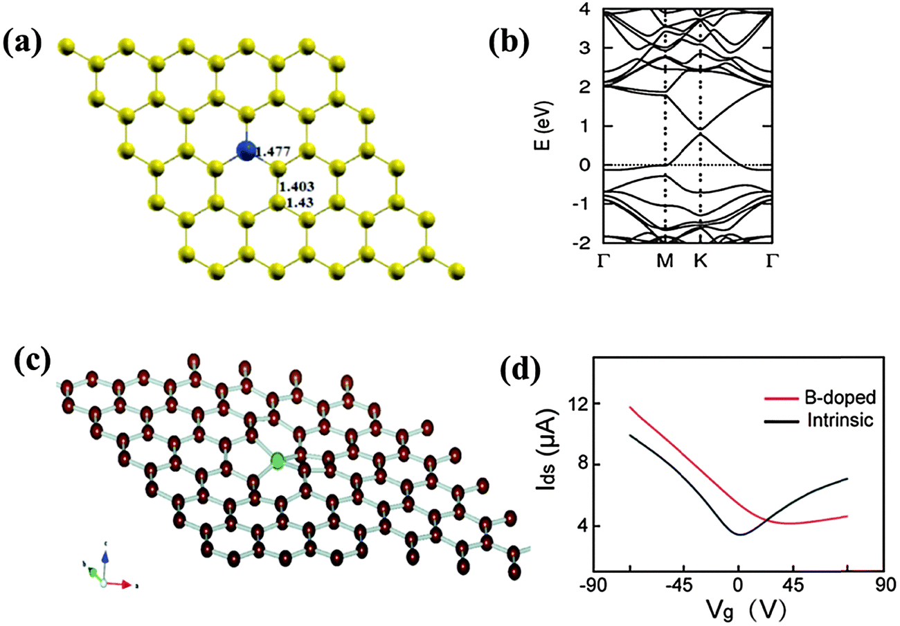 | ||
| Fig. 9 (a) Substitutional doping of B (blue ball). (b) Band structure of a single B atom doped graphene sheet. Adapted with permission from ref. 117. Copyright (2013) Royal Society of Chemistry. (c) B atom in a divacancy with symmetric disposition. Adapted with permission from ref. 119. Copyright (2010) American Chemical Society. (d) Source-drain current (Ids) vs. back gate voltage (Vg) with Vds = 0.1 V of B-doped (red) and pristine (black) graphene device. Adapted with permission from ref. 36. Copyright (2010) Wiley Publishing Group. | ||
Heteroatom doping offers possibilities for tailoring the electronic properties of graphene. The electron-deficient nature of B induces a p-doping effect accompanied with a downshift of the Fermi level towards the Dirac point (Fig. 9b).117 It has been predicted that the Fermi level decreases to ∼0.65 eV with 2 at% graphitic B and even more at higher doping levels.121 Scanning tunneling microscopy (STM) and theoretical simulations show that B-doping pulls more density of states (DOS) above the Fermi level because of the hole-doping effect.118,123 It has been shown theoretically that a bandgap of 0.14 eV can be introduced by doping a B-atom into a 50-C-atom matrix, transforming graphene from a semimetal to a semiconductor.117,124 The symmetry breaking in the carbon lattice is believed to be responsible for the bandgap opening, which is maximized when the B-atoms are located at the same sublattice positions. Bandgap opening is also sensitively dependent on the doping concentration and the graphene thickness (number of layers).117,125 First-principles calculations show that B or N substitution almost does not change the linear dispersion of the electronic bands within 1 eV of the Fermi level (Fig. 9b), meaning that B- or N-doped graphene inherits some intrinsic electronic properties of graphene.117,121 However, the anisotropy caused by B-doping is not sufficient to induce localized states, and thus magnetism.119
As shown by a theoretical study, the remarkable transport properties of graphene are preserved even at a high substitutional B/N doping level of 4.0 at%.126 However, the mobility of electrons and holes (and therefore, the conductivity) becomes asymmetric with respect to the Dirac point. This is supported by the experimental observation that B-doped CVD-graphene exhibits high carrier mobility of 800 cm2 V−1 s−1 and a typical p-type conductive behavior with strong asymmetry in hole and electron conduction (Fig. 9d).36 The large Dirac point shift (∼30 V) corresponds to a hole-doping concentration of ∼2 × 1012 cm−2. The electrical conductivity of B/N-doped graphene increases with the dopant concentration in the low temperature region and decreases due to the elevated scattering effect from the impurity atoms in the high temperature region.127 Considering the remarkable difference in the electronic properties between multilayer and single-layer graphene, Guillaume et al. investigated the influence of asymmetric substitutional B/N doping on bilayer graphene.128 A smaller doping-induced Fermi level shift is observed in the bilayer because electrons and holes are shared by the neighboring carbon layers.
3.2 Group Va elements (N and P)
N is also a neighboring element to carbon in the periodic table. The electron-rich nature of N (1s22s22p3) makes N-doped graphene distinctly different from B-doped graphene. The possible bonding configurations of N dopants are shown in Fig. 10a.129 As discussed in the Synthesis Methods section, mainly three N bonding configurations exist, i.e., graphitic (or quaternary), pyridinic and pyrrolic N. Because of the similar bond lengths of C–N (1.41 Å) and C–C (1.42 Å), pyridinic and graphitic N exert a marginal influence on the graphene structure. In contrast, sp3 bonded pyrrolic N disrupts the planar structure of graphene.130 Pyridinic N bonding configuration is the most stable in the presence of monovacancy, while pyridinic and graphitic N dominate in the presence of Stone–Wales and divacancy defects.131,132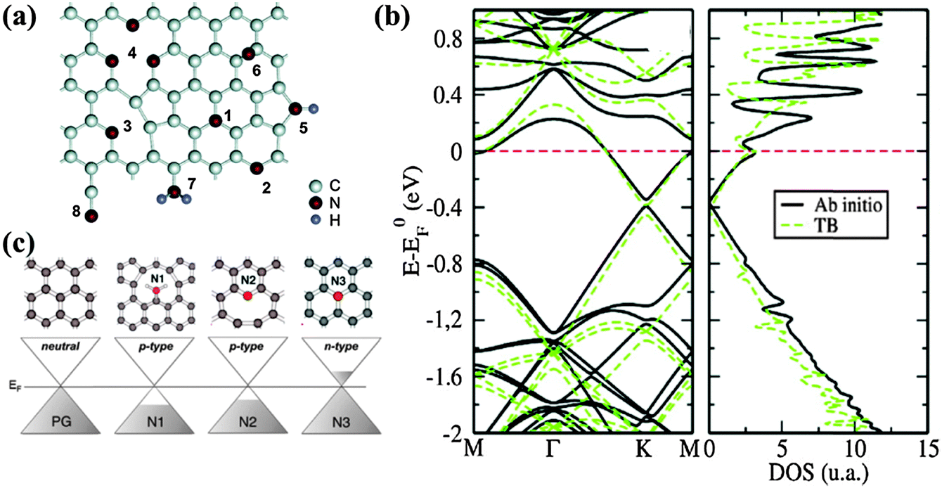 | ||
| Fig. 10 (a) Possible configurations of nitrogen dopants in graphene: 1-graphitic N, 2-pyridinic N, 3-single N pyridinic vacancy, 4-triple N pyridinic vacancy, 5-pyrrolic N, 6-interstitial N or adatom, 7-amine, 8-nitrile. Adapted with permission from ref. 129. Copyright (2011) American Chemical Society. (b) Ab initio (thick black lines) and tight-binding (green dashed lines) band structures (left) and DOS (right) of a 10 × 10 graphene supercell containing one substitutional N dopant. Adapted with permission from ref. 134. Copyright (2013) American Chemical Society. (c) Computed doping effect of N dopant for the different bond types as compared to pristine graphene. Adapted with permission from ref. 137. Copyright (2012) American Chemical Society. | ||
The larger electronegativity of N (3.04 on the Pauling scale) than that of C (2.55 on the Pauling scale) creates polarization in the carbon network, thereby influencing the electronic, magnetic and optical properties of graphene.133 N-doping opens a bandgap near the Dirac point by suppressing the nearby density of states (DOS), thereby conferring graphene with semiconducting properties (Fig. 10b).134,135 The semiconducting behavior of N-doped graphene depends on the doping configurations. For graphitic N, three valence electrons of nitrogen form three σ-bonds with the neighboring carbon atoms, one electron is engaged in a π bond formation, and the fifth electron is partially involved in the π*-state of the conduction band. Each graphitic N can contribute ∼0.5 electron to the π network of the graphene lattice, resulting in an n-doping effect.136 In comparison, pyridinic and pyrrolic N form at the defects sites, and these defects impose the p-doping effect by withdrawing electrons from the graphene sheet (Fig. 10c).137
Liu et al. demonstrated graphitic N-dominated CVD-graphene with n-type behaviour and carrier mobility of 200–450 cm2 V−1 s−1.135 Li et al. further reported crossover behaviour from the p-type to n-type with an increasing N-doping level: even the dominant species are pyridinic and pyrrolic types.138 Schiros et al. attributed this phenomenon to the hydrogenation of pyridinic and pyrrolic N, which transformed them from the p to n type.137 Usachov et al. reported a bandgap opening of ∼0.3 eV and charge-carrier concentration of ∼8 × 1012 cm−2 induced by the 0.4 at% doping of graphitic N.129 Sodi et al. theoretically showed that in contrast to doping at the basal plane, edge functional groups exert a marginal influence on the band structure of graphene.139 As shown by Ouerghi et al., only 0.6 at% graphitic N-doping results in a large carrier concentrations of 2.6 × 1013 cm−2 (4 times higher than that of pristine graphene), while pyridinic and pyrrolic N exert little influence.140
N doping has also been proven to be powerful in tuning the work function of graphene materials, which is instrumental for devices such as organic field effect transistors (OFETs) and light emitting diodes (LEDs). Schiros et al. calculated the work function of pristine graphene (4.43 eV) and graphene doped with graphitic (3.98 eV), pyridinic (4.83 eV), and hydrogenated pyridinic (4.29 eV) N.137 The change of the work function is caused by the electron donating or accepting nature of each N-bonding configuration. Consistently, Kim and co-workers confirmed the reduction of the work function by graphitic N-doping using ultraviolet photoelectron spectroscopy.141 Contradictory to the theoretical predication, Lin et al. showed that pyridinic N reduces the work function of CVD graphene.142 This discrepancy could be due to the hydrogenation of pyridinic N.137
More recently, the creation of a magnetic moment on graphene by heteroatom doping has attracted considerable research interest for spintronic applications. Due to the lack of nonbonding electrons, graphitic N is not able to generate a magnetic moment. Although both pyrrolic and pyridinic N have a non-bonding electron pair, only pyrrolic N can form π and π* states that lead to spin polarization. Therefore, pyrrolic N can create strong magnetic moments, while pyridinic N only has a weak effect.143 Furthermore, Chen et al. theoretically demonstrated that each pyrrolic N doped at the edge sites of graphene nanoribbons (GNR) produces a magnetic moment of 0.95 μB, while pyridinic N at the edges creates a magnetic moment of 0.32 μB.144
N doping can also tailor the optical properties of graphene sheets. Chiou et al. demonstrated the influence of N-doping on the photoluminescence (PL) property of graphene nanoflakes (GNF).145 When excited, the electrons of doped N can transfer energy to the π* state of the sp2 cluster of GNF. Therefore, a larger amount of energy is released when electrons fall from the π* state back to the π state, leading to higher intensity PL (Fig. 11). As demonstrated by Kim et al., pyrrolic, pyridinic and graphitic N result in the blue-shift of the PL peak, while only graphitic N is able to enhance the intensity.146 However, Tang's group reported that with 3.05 at% pyridinic-N, the PL emission of rGO is quenched by 76%, possibly because of the intramolecular energy transfer between the doped N and graphene sheet.147
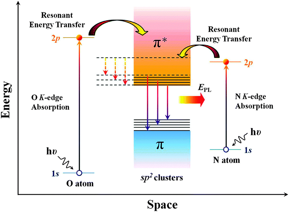 | ||
| Fig. 11 Possible mechanism of photoluminescence enhancement by resonant energy transfer from N and O dopants to the sp2 clusters in the GNFs matrix. EPL stands for the enhanced PL emission. Solid and dotted lines represent radiative (EPL) and nonradiative (low and broad PL) relaxation processes, respectively. Adapted with permission from ref. 145. Copyright (2012) American Chemical Society. | ||
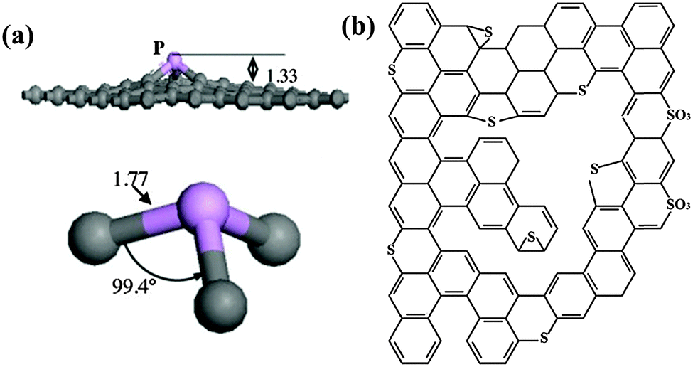
As P is larger than N, P-doping causes more structural distortion. By transforming the sp2 hybridized carbon into the sp3 state, P can form a pyramidal like bonding configuration with three carbon atoms. In such a configuration, P overhangs from the graphene plane by 1.33 Å accompanied with 24.6% increase in the P–C bond length with respect to the C–C bond length of pristine graphene (Fig. 12a).148 Unlike N, the electronegativity of the P atom (2.19) is significantly lower than that of the C atom (2.55);149 therefore, the polarity of the C–P bond is opposite to that of the C–N bond. Further, when compared with N-doping, distinct effects by P-doping may also arise from the additional orbital of P (3s23p3).
 | ||
| Fig. 12 (a) Optimized geometrical structure of P-doped graphene. The gray and pink balls represent the carbon and phosphorus atoms, respectively. The bond distances are in angstroms. Adapted with permission from ref. 148. Copyright (2013) Elsevier Publishing Group. (b) Typical configuration of S-doped graphene. Adapted with permission from ref. 82. Copyright (2012) American Chemical Society. | ||
Hirshfeld population analyses show that P can transfer 0.21e to the graphene sheet148 and graphitic N transfers 0.5e, suggesting the stronger ability of N for electron donation.150 Contrarily, it has been shown that P-doped bilayer graphene exhibits prominent n-type behaviour with 5 times higher electron mobility than pristine bi-layer graphene, while N-doped bi-layer graphene shows a weaker n-type behavior and lower mobility than pristine graphene.151 The same study also shows that unlike N-induced n-doping, the n-type behavior of P-doped graphene is retained in the oxygen atmosphere. The discrepancy between the theoretical prediction and experimental observation may be because N-doping from graphitic N is partially neutralized by the co-existing electron-accepting pyridinic and pyrrolic N.
A theoretical investigation suggests that the bandgap opening positively depends on the P-doping concentration, and a bandgap of 0.3–0.4 eV is resulted with a P-doping level of 0.5 at%.152 Similar to N-doping, P-doping can also induce a magnetic moment. Zhao et al. found that the magnetic moment of P-doped graphene is ∼1.02 μB due to the symmetry breaking of the graphene π-electron framework.148 This value is in good accordance with the DFT calculations (1.05 μB) reported by Dai and Yuan.153 P-doping is more potent than N-doping in inducing magnetic moments.
3.3 Group VIa elements (O and S)
VIa group is also known as the oxygen family, among which, oxygen is the most electronegative element. The substitutional doping of an O atom is impossible because of its strong electronegativity and large size. Graphene oxide (GO), usually oxidatively exfoliated from graphite powder, is the most studied graphene derivative. Having epoxyl (C–O–C) and carbonyl (CO) groups, GO and its reduced form (rGO) can be regarded as O-doped graphene. The covalent attachment of oxygen groups transforms sp2 into the sp3 hybridization state, accompanied by local distortions of the graphene planar structure. The extensive presence of localized sp3 domains gives rise to a bandgap opening,154,155 and together with the defects, they make GO poorly conductive or non-conductive. Excellent hydrophilicity makes GO suitable for solution processes.
It is generally assumed that a GO sheet bears hydroxyl and epoxyl groups on its basal plane and carboxyl and carbonyl groups at the edges.156 As a non-stoichiometric compound, the properties of GO highly depend on the abundance and composition of different types of oxygen groups, which are specific to synthetic processes and post-synthesis treatments.13,157 Intriguingly, the chemistry of GO changes in the ambient condition, for example, epoxyl groups may evolve to hydroxyl groups in the presence of hydrogen.158–160 The acidic and oxidative nature of abundant oxygen functionalities allow GO to function as a mild and green oxidant and catalyst. For example, GO has been reported to be capable of oxidizing substituted cis-stilbenes to their corresponding diketones and facilitating an oxygen activation reaction.161–163 As GO and rGO have already been thoroughly discussed in a number of review articles,13,164,165 in this article, we emphasize more on other heteroatom doping.
S shares similar doping configurations as O, e.g., C–S–C, C–SOx–C (x = 2, 3, and 4) and C–SH (Fig. 12b).82 The C–S bond length (1.78 Å) is ∼25% longer than that of the C–C bond.166 Consequently, a curved carbon nanostructure (e.g., carbon nanotube) favors S-doping more than flat graphene. A theoretical study has proposed that S-doping on graphene occurs in two steps: the formation of defect sites and SS bond rapture, and depending on the doping level, the resultant graphene sheet can become a small-band-gap semiconductor or more metallic than pristine graphene.167 Poh et al. experimentally measured the resistivity of S-doped graphene thermally exfoliated from graphite oxide in the presence of S-precursor.78 In general, S-doped graphene is more resistive than pristine graphene because of the free carrier trapping caused by sulfur and oxygen functionalities.
Unlike B, N, and P, negligible polarization (or charge transfer) exists in the C–S bond because of the similar electronegativity of S (2.58) and C (2.55).168 On the other hand, in contrast to the zero spin density of pristine graphene, the mismatch of the outermost orbitals of S and C induces a non-uniform spin density distribution on S-doped graphene, which consequently endows graphene with catalytic properties useful for many applications (e.g., oxygen reduction reaction, ORR).82,83 Using first-principles calculations, Jeon et al. found that covalently bonded S and oxidized S at both the zigzag and armchair edges of graphene nanoplates (SGnPs) obtained from ball milling can induce a significant spin density increase.82 In addition, the oxidization of SGnPs further enhanced their catalytic activity, accompanied by 5–10 times increase of magnetic moments. The same study also showed that the highest occupied molecular orbital (HOMO) and lowest unoccupied molecular orbital (LUMO) of graphene are strongly polarized by edge-sited S dopants, leading to high catalytic activity towards ORR. In contrast to the extensive studies on O- and S-doping, there are only a few reports on Se-doping.80 The properties of Se-doped graphene remain largely unexplored.
3.4 Group VIIa elements (F, Cl, Br and I)
As is well known, halogens possess higher reactivity than group IIIa–VIa elements. As halogen-doping transforms sp2 carbon bonding to the sp3 state, it results in drastic distortions in the geometric and electronic structures of graphene. As F is one of the most reactive elements, F-bonding is strong and inert. The F–C bond in F-doped graphene sticks out the basal plane (Fig. 13a),111 and it stretches the C–C bond length to 1.57–1.58 Å.169 First-principles calculations suggest that the high affinity of F towards C enables the negative chemisorption energy of F on graphene even at the full coverage of F atoms ([CF]n, which is called fluorographene).170 For fluorographene, F is covalently bonded to sp3 C, and the graphene sheet is buckled as the F attachment alternates on both the sides of the graphene sheet (i.e., basal plane is sandwiched by two F-layers). Fluorographene has attracted a great deal of attention because of its extraordinary mechanical strength, high thermodynamic stability and superb chemical inertness.169,170 These properties promise the use of fluorographene, for example, as a lubricant and battery additive. Fluorographene is the thinnest insulator because of its wide bandgap of ∼3 eV, resulting from a high degree of sp3 bonding of carbon atoms (Fig. 13b).169,171,172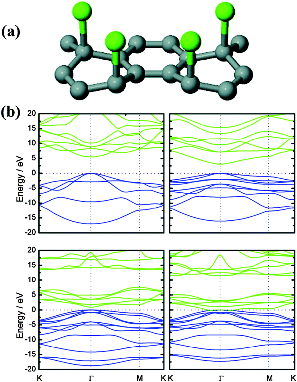 | ||
| Fig. 13 (a) Schematic illustration of partially fluorinated or chlorinated graphene structure. Adapted with permission from ref. 111. Copyright (2011) American Chemical Society. (b) The electronic band structure of CH, CF, CCl, and CBr along lines connecting the high-symmetry points K, Γ and M in the Brillouin zone. The zero-energy level has been set to the valence band maximum. Adapted with permission from ref. 169. Copyright (2010) Wiley Publishing Group. | ||
F-doped graphene can be employed as semiconductors with a bandgap tunable by the F-coverage98 and with luminescence ranging broadly from the ultraviolet to visible light regions.173 Obtained by exposing only one-side of CVD graphene to xenon difluoride, single-sided F-doped graphene (25% F coverage, C4F) is optically transparent with a bandgap of 2.93 eV and over 6 orders of increase in resistance when compared with pristine graphene.171 Further, F-doping increases the hydrophobicity of graphene.116
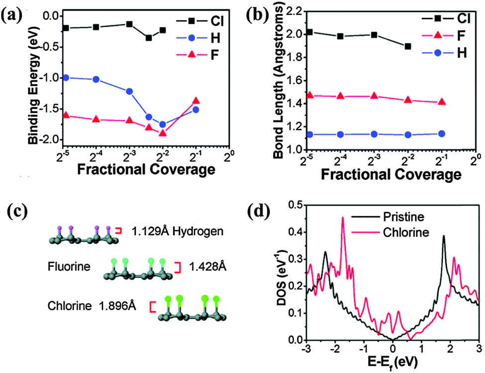
In the case of Cl-doped graphene, ab initio simulations show that Cl atoms on graphene have a lower binding energy and longer bond length than that of F and H, suggesting that the covalent Cl–C bond is less stable than C–F and C–H bonds (Fig. 14a–c).111 Because of the long bond length, Cl-doped graphene (1.1–1.7 nm) is thicker than F-doped graphene.113 In addition to the similar bonding arrangement as F (Fig. 13a), Cl can interact with C via forming charge-transfer complex, covalent bonding, and physical absorption as suggested by DFT calculations.130 Further, 25% coverage of covalently bonded Cl (C4Cl) creates a bandgap of 1.4 eV. At full coverage of Cl, Br and I, non-covalent interaction is more stable.174,175 The full coverage of Cl (like fluorographene) is controversial. It has been theoretically proposed that alternative covalent bonding on both the sides allows full Cl coverage: even at full coverage, the graphene bandgap is only opened to ∼1 eV (Fig. 13b).169 However, Sahin et al. reported that the dense decoration of Cl on a graphene surface leads to the desorption of Cl in the form of Cl2 due to a stronger Cl–Cl interaction.176
 | ||
| Fig. 14 (a) Binding energies and (b) bond lengths of the C–X bond (X = Cl, H, F) as functions of coverage, based on ab initio simulations. (c) Atomistic structures and bond lengths of C–X. (d) Calculated DOS of graphene with a 1/30 coverage of Cl atoms in comparison with that of pristine graphene as a function of energy E − EF, where EF is the Fermi energy. Adapted with permission from ref. 111. Copyright (2011) American Chemical Society. | ||
Cl is a p-dopant (Fig. 14d). Zhang et al. successfully synthesized Cl-doped graphene with a high Cl coverage of 45.3% (close to C2Cl), which was stable over one week under ambient conditions.112 Hall-effect measurements reveal the p-doping effect and a high hole concentration of 1.2 × 1013 cm−2 (increase of ∼3 times) (Fig. 15). In comparison with the carrier mobility decrease of F-doped graphene from 1060 cm2 V−1 s−1 to about 5 cm2 V−1 s−1,171 Cl-doping preserves a high carrier mobility of 1535 cm2 V−1 s−1.112 In addition, Cl-doping enhances the conductivity of graphene by 2 times (Fig. 15). Owing to the low binding energy, Cl-doping and Br-doping start to decompose at a low temperature (<400 °C) and completely evaporate at a temperature of >600 °C.99
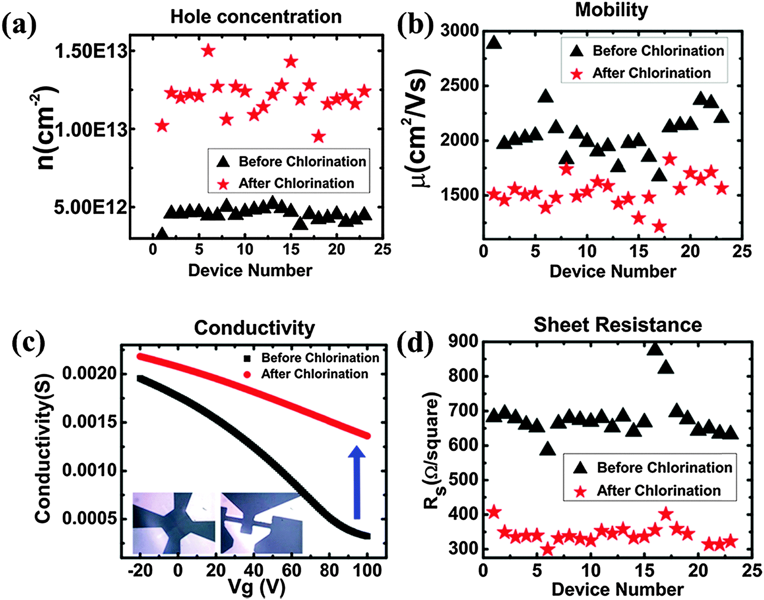 | ||
| Fig. 15 Chlorination changes the transport properties of graphene. (a) Carrier concentration. (b) Mobility. (c) Electrical conductivity. (d) Sheet resistance. Adapted with permission from ref. 112. Copyright (2013) American Chemical Society. | ||
In contrast to the extensive research efforts spent on F- and Cl-doping, there are only a few theoretical and experimental reports on Br- or I-doped graphene. This is due to the thermodynamic instability correlated with their large sizes and low electronegativity (F = 3.98, Cl = 3.16, Br = 2.96 and I = 2.66). Unlike F and Cl, large-sized halogen atoms (Br and I) are likely to interact with graphene only via physisorption or charge-transfer complex formation, without disrupting the sp2 carbon network.174,177 As shown in Fig. 13b, brominated graphene is an indirect gap material with almost zero bandgap. In comparison, hydrogenated, fluorinated and chlorinated graphene materials are direct bandgap materials.169 Further, DFT studies reveal the metallic behaviors of Br- or I-doped graphene materials.169,174 The electronegative and chemically reactive properties of I facilitate its easy aggregation to form linear polyiodide anionic species (e.g. I3− and I5−) on the graphene surface.46,85
3.5 Other dopants
Graphene hydrogenation via sp3 C–H bond can transform zero bandgap graphene into a wide-gap semiconductor.178,179 Many studies have been conducted on the structural, electronic and magnetic properties of fully or partially hydrogenated graphene.180–182 However, because of the small difference in the electronegativity between C and H, the C–H bond is essentially non-polar, and therefore, non-reactive. This largely limits the practical applications of hydrogenated graphene materials.The doping of metallic atoms has rarely been demonstrated experimentally. This is probably because the binding energy between these elements with graphene is much lower than their cohesive energy. Consequently, they tend to form clusters instead of being uniformly doped on the graphene surface.183 In addition, large-sized metal atoms can create a larger local curvature, favoring the chemisorption of small molecules from the ambience (e.g., H2O, O2, NO), which greatly limits the practical applications of such doped graphene.184,185
Silicon (Si), which belongs to the same group as C, is a tetravalent metalloid. The much longer bond length of Si–C (1.75 Å) with respect to the C–C bond forces the Si atom to protrude from the graphene plane, accompanied with remarkable distortion of the graphene planar structure. The created disorders make Si-doped graphene promising as a metal-free catalyst for CO oxidation,186 ORR,187 NO and NO2 reduction.188,189 However, the experimental reports on Si-doped graphene are rare. This may, at least in part, be attributable to the strong chemisorption of the ambient molecules,190 which unavoidably change the intrinsic properties of Si-doped graphene.
3.6 Co-doping
The co-doping of multiple species of foreign atoms may generate new properties or create synergistic effects. B and N atoms are similar in size and produce opposite doping effects on graphene. While being simultaneously doped onto graphene, boron nitride (BN) domains tend to form due to the phase separation between C and BN (Fig. 16a).33,191–194 This is attributed to the larger binding energy of B–N and C–C than that of B–C and N–C bonds. B,N co-doping leads to four bonding configurations, i.e. C–C, B–N (dominating form), C–B and C–N with bond lengths of 1.42 Å, 1.45 Å, 1.49 Å and 1.35 Å, respectively.193 Strong charge polarization exists between B and N,193,195 which yields active surface chemistry. The thermal stability of B,N co-doped graphene is lower than N-doped graphene, but higher than B-doped graphene.35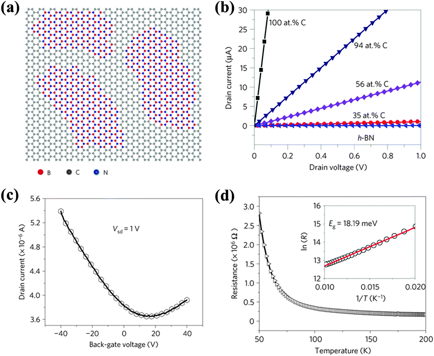 | ||
| Fig. 16 (a) Atomic model of the h-BNC film showing hybridized h-BN and graphene domains. Scale bars: 2 nm. (b) Current–voltage (I–V) characteristics of as-grown BNC with different percentages in carbon measured at room temperature. (c) The drain current as a function of the voltage applied to the back gate for a 7 μm-wide BNC ribbon with 40% carbon. The drain–source voltage is fixed to 1 V. (d) Resistance vs. temperature curve for a typical h-BNC ribbon with a width of 5 μm and a length of 11 μm. The inset shows ln(R) as a function of T−1 in the temperature range from 50 to 100 K. Adapted with permission from ref. 33. Copyright (2010) Nature Publishing Group. | ||
The co-doping of B and N on graphene by CVD produces a sp2 hybridized hexagonal lattice with BN domains (B/N ratio = 1) surrounded by graphitic domains.33 The conductivity of such films (h-BNC) is tunable from insulating to highly conductive depending on the C percentage (Fig. 16b). Similar to previously reported BC2N thin-film,196,197h-BNC exhibits a p-type semiconducting behavior with electron and hole mobility of 5–20 cm2 V−1 s−1 (Fig. 16c). The reduced mobility is attributed to the electron scattering at the boundaries between BN and C domains. Based on the temperature-dependent resistivity of h-BNC (with 56 at% C), a small bandgap (18 meV) is predicted (Fig. 16d). Asymmetric B,N doping (B7.8N4.7C87.5) moderately increases the bandgap (0.49 eV) because of symmetry breaking.198 It has been shown that at an appropriate B/N ratio, the HOMO–LUMO energy gap of graphene may be reduced, leading to enhanced chemical reactivity.69 Both B and N doping creates a bandgap at the Dirac point, but they shift the Fermi level in opposite directions. Uniform B,N co-doping (although it is difficult to experimentally realize) is believed to open a bandgap at the Dirac point without shifting the Fermi level.193,199,200 As suggested by DFT studies, the opened bandgap increases with the size of the BN domains, regardless of their shapes.195
In contrast, random and scattered distribution of foreign atoms is observed in the case of S,N or P,N co-doping.45,201 Crosstalks between the co-dopants may affect their bonding configurations. For example, the co-doping of P may promote the pyridinic bonding of N on graphene.201 Pyrrolic N dominates in N-doped graphene, whereas the co-doping of S makes graphitic N dominant.45
4 Applications
Doping by a range of heteroatoms with varying configurations and doping levels endows graphene with a wide spectrum of new properties, for example, bandgap opening, charge polarization between heteroatom and C atom, magnetic moment, hydrophilicity, increased spin density, catalytic activities, etc. Doped graphene materials are, therefore, useful for various applications including energy storage, energy conversion, sensing, and gas storage (Table 2).| Applications | Materials | Advantages of doping effects | Ref. |
|---|---|---|---|
| Supercapacitors | B/N/P doped graphene | Enhanced electrochemical activity; lower charge-transfer resistance; better sheet-to-sheet separation; improved conductivity than GO precursors. | 203, 206 and 207 |
| B,N co-doped graphene | 101 | ||
| N-doped graphene/MnO2 | 211 | ||
| Lithium ion batteries | B/N/P doped graphene | Achieving balance between Li binding and diffusion; enable abundant and uniform loading of metal oxide nanoparticles. | 59 and 224 |
| N,S co-doped graphene | 225 | ||
| N doped graphene–SnO2/MnO/TiO2/VO2/Zn2GeO4/α-Fe2O3 | 106, 226–230 | ||
| Fuel cells (cathode for ORR and anode of DMFC) | B/N/P/S/halogen doped graphene | Induced charge polarization and spin density enhances oxygen adsorption and cleavage; enable abundant and uniform loading of metal nanoparticles. | 43–47, 51 and 53 |
| N,B/N,P/N,S co-doped graphene | 69, 80 and 201 | ||
| N doped graphene–Pt NW/PtRu | 81 and 251 | ||
| Solar cells (DSSC and heterojunction solar cell) | B/N/F doped graphene | Increases the catalytic activity of DSSC counter electrode; endows graphene with p or n doping effect; increases graphene work function. | 32, 254 and 257 |
| Sensors (electrochemical, electronic and SERS sensors) | B/N/P/Si/S doped graphene | Facilitates charge transfer, analyte adsorption and activation; assists anchoring of functional moieties or molecules; opens graphene bandgap; induces charge polarization. | 39, 262, 263, 269 and 275 |
| B,N/S,N/Si,N co-doped graphene | 261, 266 and 272 | ||
| Gas storage | B/N doped graphene | Increases binding affinity towards gas molecules; enables abundant and uniform loading of metal nanoparticles. | 277, 281 and 282 |
4.1 Supercapacitors
Due to their high power density and long lifecycle, supercapacitors have been intensively researched as energy storage devices. Graphene, which has the highest specific surface area, offers large electric double-layer capacitance (EDLC). However, chemically inert pristine graphene is not able to provide electrochemical capacitance (pseudocapacitance). Hence, doped graphene materials are promising for supercapacitors because of the preserved large EDLC, improved wettability, and existence of pseudocapacitance.202It has been shown that the abundant oxygen groups on rGO enhance its specific capacitance to 189 F g−1.203 When compared with O-doped graphene, graphene materials doped with B, N and P are more advantageous because of their better conductivity, stability, chemical reactivity, and sheet-to-sheet separation. A porous B-doped graphene structure synthesized by annealing frozen GO–boric acid composite shows a specific capacitance of 281 F g−1.60 N-doped graphene hydrogel (5.86 at% N with dominant pyrrolic N) synthesized by the hydrothermal method yields a large specific surface area of ∼1500 m2 g−1 and a high specific capacitance of 308 F g−1.100 The same study also showed that the capacitive performance of N-doped graphene not only depends on the N content but also on the doping configurations. Graphitic and pyridinic N can improve the wettability of doped graphene because of their large dipole moments. Further, graphitic N can facilitate electron transfer, thereby improving the capacitive behavior by lowering the charge-transfer resistance of the electrode at a high current density.108,204 Being electrochemically active in an alkaline aqueous solution, pyridinic and pyrrolic N offer high pseudocapacitance.100 At optimized balancing in N bonding configuration and doping level, a hydrothermally synthesized N-doped graphene (10.13 at%) achieves a specific capacitance of 326 F g−1 and excellent cycling stability (99.85% columbic efficiency after 2000 cycles).205
Jeong et al. fabricated a N-doped graphene-based flexible (wearable) supercapacitor that exhibits 4 times larger capacitance than its pristine graphene-based counterpart, in both aqueous and organic electrolytes (Fig. 17).108 Theoretical calculations suggest that pyridinic N at the basal plane plays a major role for capacitance improvement due to its large binding energy with K+. On the other hand, the strong ionic bonding between negatively charged pyrrolic, and K+ is predicted to be disadvantageous for the reversible charge–discharge process (Fig. 17). Fan et al. synthesized a N-doped graphene (8.7 at%) hollow structure by a thermal annealing of layer-by-layer composited GO, PANI and polystyrene nanospheres.206 Attributable to the synergistic effect of N-doping and hollow-sphere structure, it exhibits a high specific capacitance even at high current densities (381 F g−1 at 1 A g−1; 282 F g−1 at a high current density of 20 A g−1) and outstanding cycling stability (96% retention after 5000 cycles).
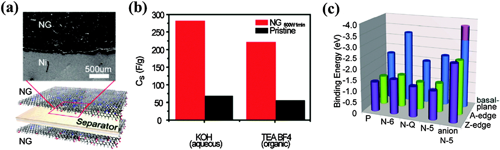 | ||
| Fig. 17 Ultracapacitors based on N-doped graphene and their electrochemical testing. (a) A schematic illustration of the assembled supercapacitor structure alongside a scanning electron microscopy image, showing the top view of the device. (b) The specific capacitances measured in aqueous and organic electrolytes. (c) The binding energies between potassium ions and N-configurations at basal planes and edges, which were calculated by first-principles DFT. “P, N-6, N-Q and N-5” along the horizontal axis indicates “pristine”, pyrrolic, pyridinic and graphitic N, respectively. Adapted with permission from ref. 108. Copyright (2011) American Chemical Society. | ||
Rajalakshmi et al. prepared P-doped graphene by annealing rGO with phosphoric acid at 220 °C.207 Working as the supercapacitor electrode in 1 M H2SO4 electrolyte, it offers a much higher capacitance (367 F g−1 at scan rate 5 mV s−1) than rGO control.207 Phosphorus on graphene is believed to assume the oxidized form and produces pseudocapacitance. S- and halogen atom doping are also expected to enhance the capacitance of graphene-based electrodes. However, their practical applications in this regard are hindered by the complicated synthesis process, limited doping level and/or low yield. In addition, the pseudocapacitive behaviors from these dopants are unclear. A few S-doped activated carbon materials have been reported for supercapacitor applications, and sulfone and sulfoxide species formed have been proposed to participate in the redox faradic reactions during the charge–discharge process.208,209
Wu et al. synthesized 3D B,N co-doped graphene aerogel (BN-GA, ∼0.6 at% B and ∼3.0 at% N) as an additive-free monolithic composite for an all-solid-state supercapacitor (Fig. 18).101 This electrode (with a capacitance of 239 F g−1) outperforms the counterpart electrodes without doping or doped with only B or N because of the synergetic effects between the two co-dopants. The solid-state supercapacitor equipped with such an electrode achieves a high energy density of ∼8.7 W h kg−1 and power density of 1650 W kg−1. O, N and Cl triply-doped rGO (16.36 at% O, 1.46 at% N mainly as pyridinic N, 1.1 at% Cl mainly as C–Cl or C–ClO) has been prepared by the anode polarization of rGO film in nitrogen-deaerated 1 M KCl solution.210 These electron-rich dopants largely increase the electrode capacitance as compared with a rGO based electrode. Heteroatom doping not only enhances the capacitance of graphene materials, but also facilitates the uniform and abundant loading of pseudocapacitive metal oxides via serving as nucleation and anchoring sites. Yang et al. synthesized a composite of N-doped graphene and ultrathin MnO2 sheet by the hydrothermal method and found a specific capacitance increase from 218.8 to 257.1 F g−1 and improved the cycling stability after N-doping.211
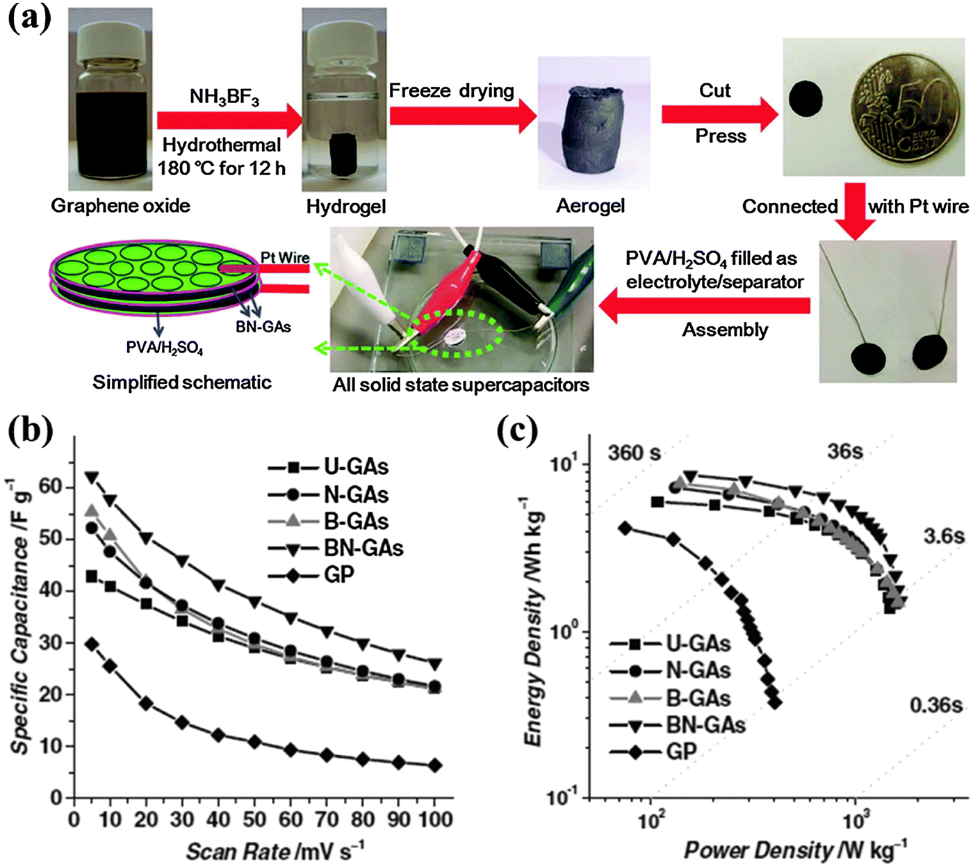 | ||
| Fig. 18 (a) Fabrication of all-solid-state supercapacitor (ASSS) based on B,N-GAs that were produced by a combined hydrothermal process and freeze-drying process. (b) Specific capacitance of undoped GAs (U-GAs), N-GAs, B-GAs, BN-GAs, and graphene paper (GP) based ASSSs on the basis of two-electrode mass as a function of scan rates from 1 to 100 mV s−1. (c) Ragone plot of ASSSs based on U-GAs, N-GAs, B-GAs, B,N-GAs and GP. Adapted with permission from ref. 101. Copyright (2012) Wiley Publishing Group. | ||
4.2 Lithium ion batteries
Lithium ion batteries (LIB) are energy storage devices with a high energy density. However, they have a relatively low power density and poor cycling stability. Pristine graphene is not suitable for Li storage due to (1) its low binding energy towards Li atoms (hence, adsorbed Li atoms tend to cluster on the graphene surface) and (2) high energy barrier for Li to penetrate through the graphene sheet.212,213 The existence of defects enables Li penetration and prevents Li clustering due to the strong interaction between Li and defect sites.213,214 On the other hand, the abundant defect sites not only compromise the mechanical robustness and electrical conductivity of graphene, but also limit the lateral diffusion of Li.215Heteroatom doping could be instrumental to optimally balance Li storage and diffusion for graphene-based electrodes.216 A partial density of states (PDOS) study suggests that a Li atom as a potent electron donor is fully ionized on graphene and interacts with graphene mainly by ionic bonding.217 Graphene substitutionally doped with B atoms is an electron-deficient system, which is desirable for improving the storage capacity of electron-donating Li.217,218 However, the enhanced binding energy between Li and B-doped graphene limits Li diffusion (and therefore, the delithiation process).217,219 In contrast, graphene doped with electron-rich graphitic N shows more efficient delithiation because of the electrostatic repulsion between N and Li.212,217 However, this comes at the price of reduced Li storage capacity due to the lowered binding energy.220 Altogether, graphitic B doping promotes LIB capacity, whereas graphitic N doping improves the charge/discharge rate performance. Both these graphitic doping procedures are not able to enhance the penetration of Li through graphene sheets (perpendicular diffusion).213
Pyridinic and pyrrolic N formed at the edges and defect sites can promote the perpendicular diffusion of Li.213,221 In addition, Cao et al. theoretically showed that pyridinic and pyrrolic N have a higher binding energy with Li than that with graphitic N, which is favorable for increasing the storage capacity.216 On the other hand, the strong coulombic attraction between pyridinic/pyrrolic N and the adsorbed Li+ hinders the delithiation process.213 A theoretical study shows that N-doping at divacancy defects facilitates perpendicular penetration, while doping at both monovacancy and divacancy has the desired binding energy to optimally balance the binding capacity and delithiation of Li.213
Experimental investigations have been conducted to explore the potential of B- or N-doped graphene as an LIB anode. Reddy et al. reported a CVD-grown N-doped graphene (9.0 at%) anode that achieves a higher reversible discharge capacity (0.05 mA h cm−2) than that of pristine graphene.37 The improved performance is benefited from the dominant pyridinic N species and N-doping induced topological defects. Wang et al. synthesized N-doped graphene (∼2 at%) by thermally annealing GO in NH3, which offers a high reversible capacity of 900 mA h g−1 (5 times higher than that of pristine graphene) with an excellent rate performance.68 Using a similar annealing method, Wu et al. prepared B-doped (0.88 at%) and N-doped (3.06 at%) graphene, which gave high reversible capacities of 1549 or 1043 mA h g−1 with superior high rate performances, respectively.59 These B- and N-doped graphene anodes also exhibit excellent energy (∼34.9 kW kgelectrode−1 and ∼29.1 kW kgelectrode−1) and power densities (∼320 W h kgelectrode−1 and ∼226 W h kgelectrode−1), respectively, which are much higher than that of pristine graphene. The improved performance is attributed to the increased conductivity, chemical reactivity, and wettability, resulting from heteroatom doping.
The doping of other heteroatoms (e.g. O, Si, P, and S and halogen atoms) has also been reported to enhance the LIB performance. The oxygen groups (e.g. carbonyl, ester, carboxylic, epoxide and hydroxyl groups) on GO or rGO can enhance the capacity of LIB via Faradaic reaction with Li, for example, Li+ + CO + e− ↔ C–O–Li.222,223 However, their instability at high current densities compromises the rate performance of LIB.59 Theoretical calculations show that the binding of Li to B, Si, and P dopants (but not N and S) are energetically favored.212 Hou et al. reported a P-doped graphene (1.32 at%) anode with a higher reversible capacity (∼460 mA h g−1) than that of pristine graphene.224 The authors attributed this improved performance to the topological defects caused by P doping. Wang et al. fabricated a 3D N,S co-doped graphene hieratical structure (4.2 at% N and 0.94 at% S) as an LIB anode (Fig. 19).225 Owing to the synergistic effects between the 3D structure and co-dopants, such LIB exhibits an excellent rate performance and a high reversible capacity of 1137 mA h g−1, which is ∼3 times the theoretical capacity of graphite and much higher than pristine graphene.
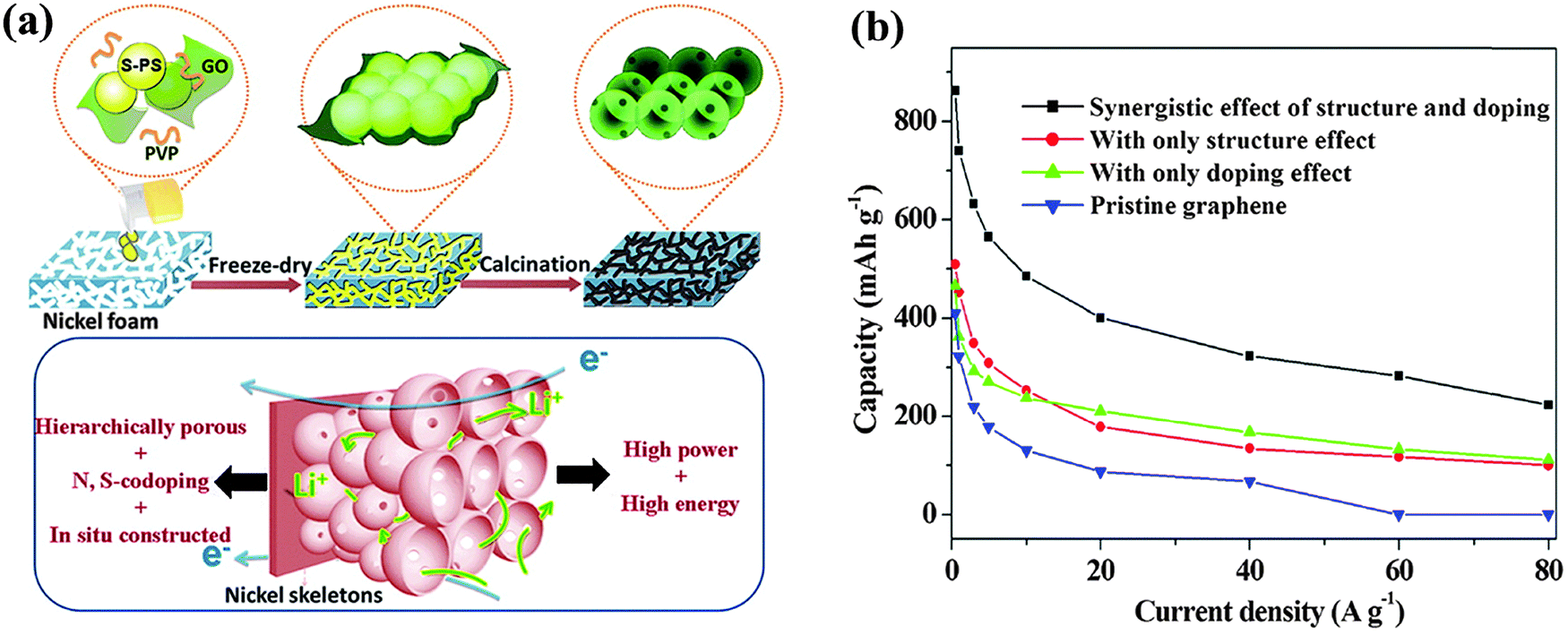 | ||
| Fig. 19 (a) Schematic illustration of synthesis procedures of 3D N,S co-doped graphene hieratical structure. (b) Comparison of lithium storage performance of pristine graphene and graphene with different effects. Adapted with permission from ref. 225. Copyright (2013) American Chemical Society. | ||
Heteroatom doping can be utilized for the anchoring of nanostructured metal oxides (e.g. SnO2,226 MnO,227 TiO2,228 VO2,106 Zn2GeO4229 and α-Fe2O3230) in order to improve the LIB performance. For example, a sandwich paper of N-doped graphene (8 at%) and SnO2 provides a higher capacity (918 mA h g−1) than pure SnO2 nanoparticles or graphene paper.226 In addition to serving as the conducting network, the intercalated N-doped graphene sheets also prevent the aggregation of SnO2 nanoparticles and provide an elastic buffer space for the volume change of SnO2 nanoparticles during Li-ion insertion/extraction process, which is crucial for high rate performance and cycling stability.
4.3 Fuel cells
Developing a state-of-the-art electrocatalyst system with mass-produced and cost-effective materials is pivotal to underpin the industrial operation of fuel cells, in which the sluggish cathodic oxygen reduction reaction (ORR) is often the rate-limiting step. Theoretical and experimental studies have shown that pristine graphene lacks catalytic activities towards ORR and is not efficient in facilitating electron transfer.231 The deliberate doping of graphene with alien atoms (especially B and N) can transform it to an effective metal-free electrocatalyst for ORR. An electrocatalytic ORR process, depending on the catalyst surface chemistry, often involves complex multiple steps and various adsorbed intermediates. As for the ideal four-electron pathway, oxygen is firstly chemisorbed on the catalyst surface followed by reducing into OH−. B, N and P dopants promote the adsorption of oxygen and O–O bond cleavage because of the charge polarization of the heteroatom–C bond.232–236 The catalytic ability of S- or Se-doped graphene originates from the creation of spin density due to orbital mismatch between these heteroatoms and C.53,82 In some cases, a charge polarization and spin density increase may simultaneously contribute (e.g., for N-doped graphene).41,80,237,238The wrinkles and surface tension induced by large-sized dopants also enhance the ORR kinetics by promoting charge transfer.239,240 The binary doping of impurity atoms into graphene (e.g. B–N,69,201,236 P–N,201 N–S/Se45,80,95) reveals the synergistic effects from different co-dopants on the ORR parameters (e.g. onset potential, current density and electron transfer number). A more thorough discussion on B-, N-, P-, S- and Se-doped graphene or other carbon materials for ORR applications can be found in several excellent review articles.29,241,242
Halogen-doped graphene for ORR is much less explored albeit its interesting physicochemical and electrical properties. Jeon et al. synthesized a series of halogenated graphene nanoplates (XGnPs, X = Cl, Br, or I) by a simple ball milling technique and investigated their electrocatalytic performance towards ORR.51 Halogen atoms are selectively doped at the edge of GnP with a doping level of 5.89 at% Cl, 2.78 at% Br and 0.95 at% I, respectively. As shown in Fig. 20a, the ORR performance of XGnPs increases in the order of IGnP > BrGnP > ClGnP, which is contrary to the order of the dopant's electronegativity: Cl (3.16) > Br (2.96) > I (2.66). The excellent performance of IGnP (∼3.9 electrons) is close to the ideal four-electron process. DFT calculations show that substitution bonding at the zigzag edge (e.g. –Cl+–, –Br+–, –I+–) are favorable for O2 adsorption and O–O bond weakening, as evidenced by the increased bond length (Fig. 20c). This is also attributable to the charge transfer between the halogen and O2, the efficiency of which follows the order of Cl < Br < I. In addition to the enhanced catalytic activity, heteroatom doping may also improve the long term stability, selectivity, tolerance to methanol and CO, and electrochemical window (Fig. 20b). Therefore, doped graphene materials are promising to replace the currently used precious metal catalysts (e.g., Pt). Yao et al. reported the excellent ORR performance of I-doped graphene synthesized by simple thermal annealing, which exhibited comparable onset potential, but higher current density as compared with Pt/C electrode.85 I3− induced charge polarization is believed to play a critical role. The ORR performance of doped graphene could be further enhanced by hybridizing it with other catalysts (e.g., Fe3O4 or Co3O4103,243).
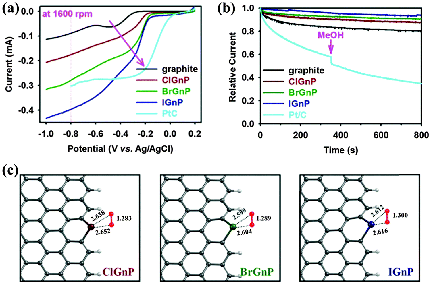 | ||
| Fig. 20 (a) Linear sweep voltammograms (LSV) at a rotation rate of 1600 rpm and a scan rate of 10 mV s−1, showing a gradual increase in current and a positive shift in the onset potential along the order of the pristine graphite, ClGnP, BrGnP, IGnP, and Pt/C (pink arrow). (b) The current–time (j–t) chronoamperometric responses for ORR for pristine graphite, XGnPs, and commercial Pt/C electrocatalysts in an O2-saturated 0.1 M aq. KOH solution at −0.40 V vs. Ag/AgCl and 3.0 M methanol or carbon monoxide (CO, 10 ppm min−1) were added at around 360 s. (c) The optimized O2 adsorption geometries onto XGnPs, where halogen covalently linked to two sp2 carbons. The O–O bond length and the shortest C–O bond are shown in angstroms. Adapted with permission from ref. 51. Copyright (2013) Nature Publishing Group. | ||
Despite the tremendous progress in the use of doped-graphene materials as a metal-free catalyst, the mechanisms of doping induced ORR enhancement is still not completely understood. In fact, some theoretical and experimental results are contradicting to each other,65,70,71,74,244–246 resulting from the large heterogeneity in the properties and structures of doped-graphene materials obtained from the current synthesis methods. The possible existence of a trace amount of metal species introduced by the synthesis procedures may also affect the ORR performance and hence, lead to misinterpretation.58,247,248 The understanding of binary and ternary doped graphene materials is even more challenging.
Doped graphene materials have also been employed as anode materials, especially in direct methanol fuel cells (DMFC). Heteroatom-doped graphene with uniform and dense decoration of precious metal catalysts can improve the catalytic activity and durability of the electrode.249 Wang et al. used S-doped graphene/Pt nanowire composite (S-doped graphene/PtNW) as both the cathode for ORR and anode for methanol oxidation reaction (MOR) (Fig. 21a and b).81 Towards ORR, it exhibits a higher current density and a lower reduction potential than the state-of-the-art Pt/C catalyst (Fig. 21c). In the case of MOR, the S-doped graphene/PtNW electrode gives ∼3 times higher peak current density in comparison with Pt/C electrode (Fig. 21d). N-doped graphene–CNT hybrid with coated PtRu has also been used as a DMFC anode, which offers a higher (>2 times) power density than the commercial PtRu/C catalyst.250 N dopants facilitate PtRu immobilization, rendering a better stability in MOR. The outstanding MOR electrocatalytic performance has also been observed for Pt- and PtAu-modified N-doped graphene materials.251
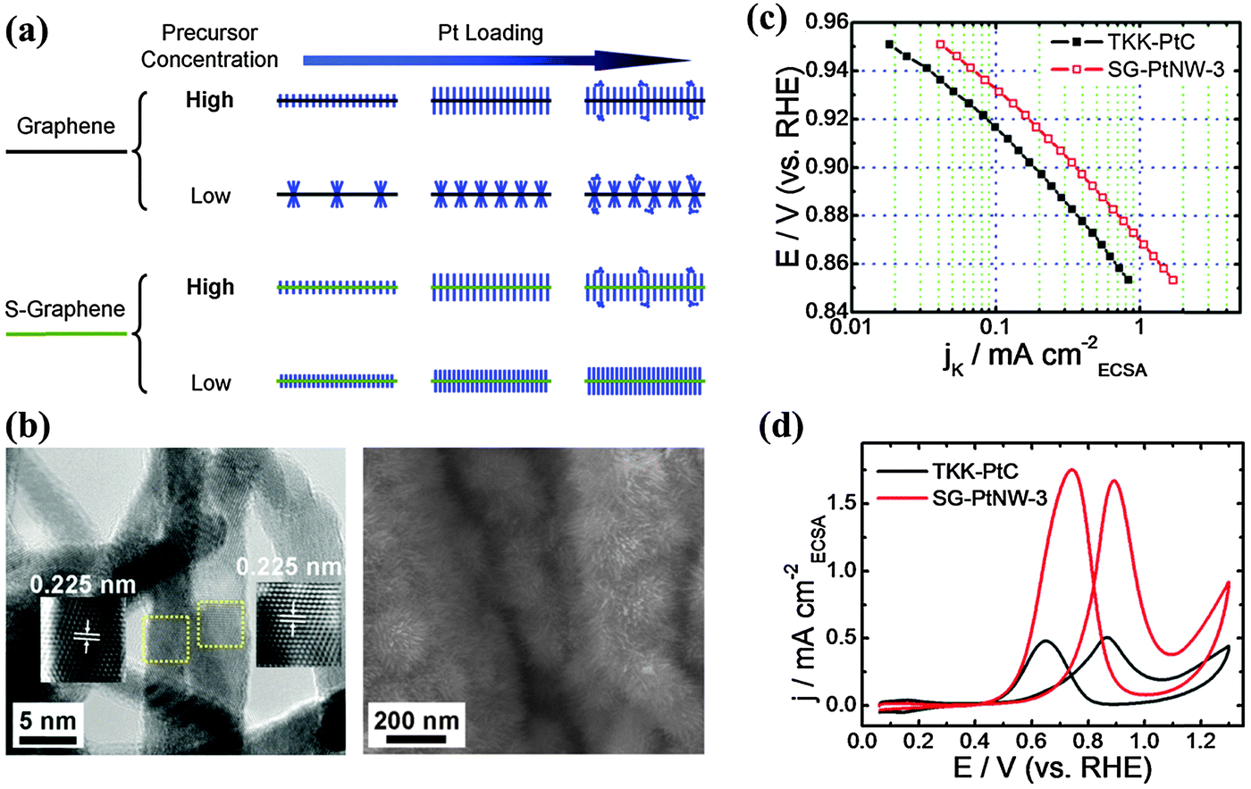 | ||
| Fig. 21 (a) Schematic illustration of the nanostructural evolution of Pt nanowire arrays grown on graphene and S-doped graphene supports. (b) SEM and high resolution TEM images of S-doped graphene/PtNW catalyst. (c) Specific kinetic current densities (jk) of S-doped graphene/PtNW and Pt/C catalysts for ORR at different potentials. (d) Specific current densities of S-doped graphene/PtNW and Pt/C catalysts toward MOR. Adapted with permission from ref. 81. Copyright (2013) Nature Publishing Group. | ||
4.4 Solar cells
A counter electrode with an optimal balance between conductivity and electrocatalytic activity is crucial. B- and N-doped graphene materials are not only highly catalytic to triiodide reduction but also generally more conductive to rGO. Dai et al. demonstrated a DSSC equipped with a N-doped graphene (7.6 at%) foam (NGF) counter electrode that offered a PCE of 7.07% as compared to that of a Pt electrode.254 The NGF electrode exhibited a lower charge transfer resistance (Rct = 5.6 Ω) than that of a Pt electrode (8.8 Ω), indicating its superior catalytic activity towards the I3−/I− redox couple. The high porosity, good hydrophilicity and large surface of NGFs led to a higher short circuit current (Jsc = 15.84 mA cm−2), open circuit voltage (Voc = 0.77 V) and fill factor (FF = 0.58) than that of rGO foam, N-doped graphene film and rGO film. Cui et al. showed that the electrocatalytic activity of N-doped rGO was positively scaled with the doping level.255 Nitrogen bonding configuration is also important to determine the catalytic properties of N-doped graphene. Compared with pyrrolic N, pyridinic and graphitic N have better catalytic activities and decreased adsorption energy toward I−.73
Using a novel redox couple Co(bpy)33+/2+ and a counter electrode fabricated by electrostatically spraying N-doped graphene nanoplatelets (NGnPs, 2.79 at%) on FTO/glass substrate, Kim et al. demonstrated a high-performance DSSC (PCE = 9.05%, Jsc = 13.83 mA cm−2, FF = 74.2%) superior to the DSSC equipped with a Pt counter electrode (PCE = 8.43%, Jsc = 13.48 mA cm−2, FF = 70.6%) (Fig. 22).256 The lower Rct of NGnP electrode (1.73 Ω cm−2) than that of the Pt electrode (3.15 Ω cm−2) suggests the higher catalytic activity of NGnP. The counter electrode based on NGnPs prepared by the ball milling method also significantly outperforms the Pt electrode.49 F-doped graphene is also electrocatalytic to I3−/I−. Das et al. reported the enhanced electrocatalytic activity of graphene towards I3−/I− after CF4-plasma treatment because of the catalytically created active edges, and F-doping enhanced interfacial electron-transfer.257 It has also been shown that B-doped graphene can serve as the back electrode with the desired ohmic contact to improve the hole-collection ability and photovoltaic efficiency of quantum-dot sensitized solar cells.57
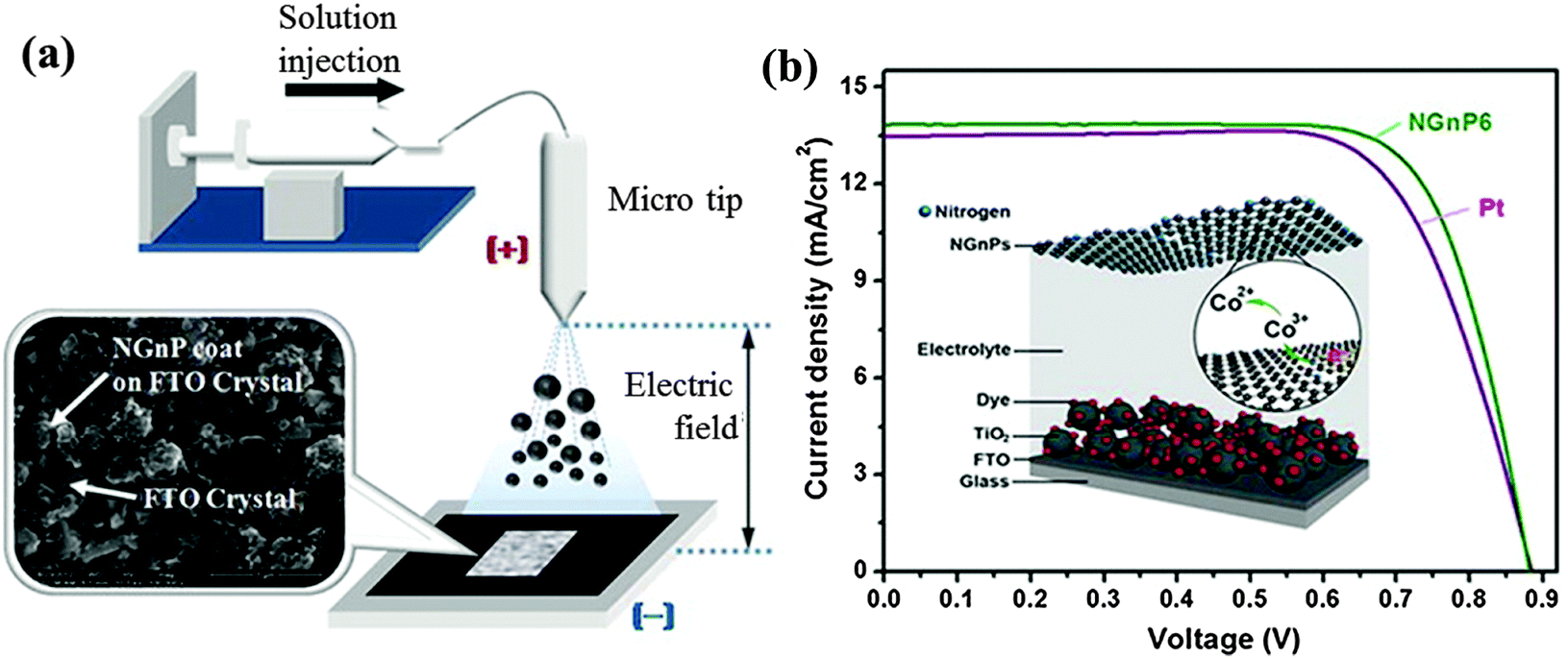 | ||
| Fig. 22 (a) Schematic representation of an e-spray setup and the SEM image of NGnP coat on FTO crystal. (b) I–V characteristics of the DSSCs with Pt and NGnP CEs under one sun illumination (AM 1.5G). Inset is the schematic illustration of DSSC with an NG counter electrode and Co(bpy)33+/2+ redox reduction on the surface of NGnPs. Adapted with permission from ref. 256. Copyright (2013) American Chemical Society. | ||
Organic solar cells (OSCs) are photovoltaic devices possibly with high flexibility, scalable fabrication process and low manufacturing cost. Bulk heterojunctions (BHJs) produced by the phase-separated blending of electron donors and acceptor materials are most commonly used in OSC devices. Heteroatom-doped graphene sheets can be used to improve conductivity, charge transfer, and thermal and chemical stability of the active layer in BHJ-OSC. Jun et al. incorporated N-doped rGO (∼8 at%) to the active layer of BHJ-OSC and found a large increase of Jsc and PCE in comparison with the device without graphene additives or with the addition of undoped rGO (Fig. 23a and b).259 N-doping induces an increase of the work function (∼0.4 eV), which, in turn, reduces the Rct value between the active polymer and graphene (Fig. 23c). The maximum PCE of ∼4.39% with Jsc of ∼14.86 mA cm−2 was obtained with 0.5 wt% addition of N-doped rGO. Overloading causes the agglomeration of graphene sheets and parasitic paths for current leakage.
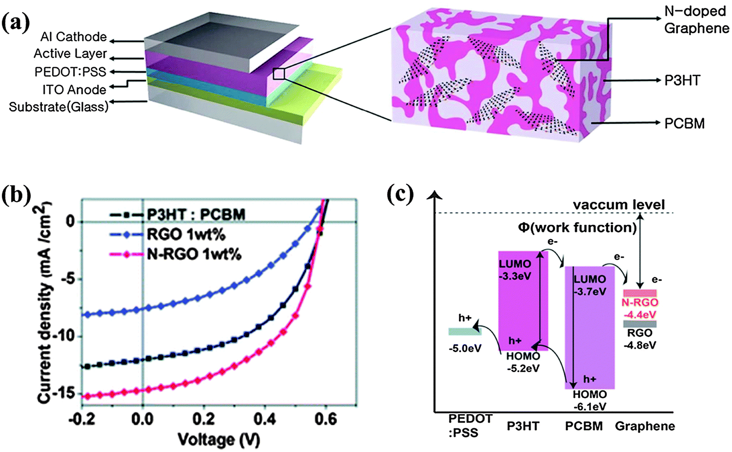 | ||
| Fig. 23 (a) Schematic of the BHJ solar cell using the N-doped graphene/P3HT: PCBM active layer. (b) I–V characteristics of BHJ solar cell devices. (c) Energy-level diagram of a rGO and N-doped RGO/P3HT: PCBM OPV, showing the charge generation and transfer between the two organic components to the electrodes. Adapted with permission from ref. 259. Copyright (2013) Royal Society of Chemistry. | ||
4.5 Sensors
Hydrogen peroxide (H2O2), which is an important signaling molecule to cells and byproduct of many biological processes, can be directly reduced by heteroatom doped graphene. Shao et al. reported an enzyme-free H2O2 sensor based on N-doped graphene electrode.260 The sensor exhibited high sensitivity and a wide linear detection range (10−5–2.8 mM) because nitrogen-induced charge delocalization weakens the O–O bond of H2O2 and the electron-donating ability of N-dopants is advantageous for the reduction reaction.
A N-doped graphene (4.5 at%) based H2O2 sensor with a wide linear range (0.5 μM–1.2 mM), low detection limit (0.05 μM), more positive onset reduction potential, and higher reduction current density was developed by Wu et al.87 The improved performance is due to the narrowed (50% reduction) HUMO–LUMO gap (and hence, higher chemical reactivity) after N-doping. Taking the advantages of the high sensitivity and specificity (against interference from other ROS species) of N-doped graphene, the authors also demonstrated the detection of the triggered release of H2O2 from live cells. Similarly, Yang et al. reported a microwave-synthesized B,N co-doped graphene sensor for the highly sensitive detection of H2O2 and its dynamic release from leukemia cells.261 The co-doped graphene outperformed (linear range: 0.5 μM to 5 mM; detection limit: 0.05 μM) the graphene sensor with single dopant only (B or N) because the charge polarization induced by B and N co-doping leads to better catalytic activity.
As the enzymatic catalysis of glucose is accompanied by the production of H2O2, N-doped graphene is also promising for glucose sensing by compositing with glucose oxidase (GOD). Wang et al. reported an amperometric sensor based on GOD/N-doped graphene electrode, with a linear detection range of 0.1–1.1 mM and detection limit of 0.01 mM.262 Owing to the high density of electronic states and active surface chemistry, N-doped graphene facilitates electron transfer from the catalytic center of GOD to the electrode surface.
N-doped graphene prepared by annealing GO with melamine was used to simultaneously and differentially detect ascorbic acid (AA), dopamine (DA) and uric acid (UA) with high sensitivity (detection limits of 2.2 μM, 0.25 μM, and 0.045 μM, respectively).263 The high sensitivity is ensured by the strong hydrogen bonding and/or π–π interaction between the N-dopants and the target molecules. Li et al. found that pyrrolic N is the most reactive to these molecules.264 N-doped graphene has also been used to electrochemically detect Bisphenol A, a widely used industrial raw material, with a detection limit as low as 5 nM.265
Guo et al. synthesized N,S co-doped graphene (6.11 at% N dominated by pyridinic N, 1.1 at% S dominated by sulfide bonds) by reducing GO using sulfate-reducing bacteria (Fig. 24).266 They were able to simultaneously detect Pb2+ (detection limit of 0.018 μg L−1) and Cd2+ (detection limit of 0.016 μg L−1), with a linear range of 9–30 μg L−1. As compared with single-species doping (N or S alone), N,S co-doping significantly improved the electrocatalytic activity towards Cd2+ (> 90%) and Pb2+ (>20%) because of the synergistic effects between the dual dopants.
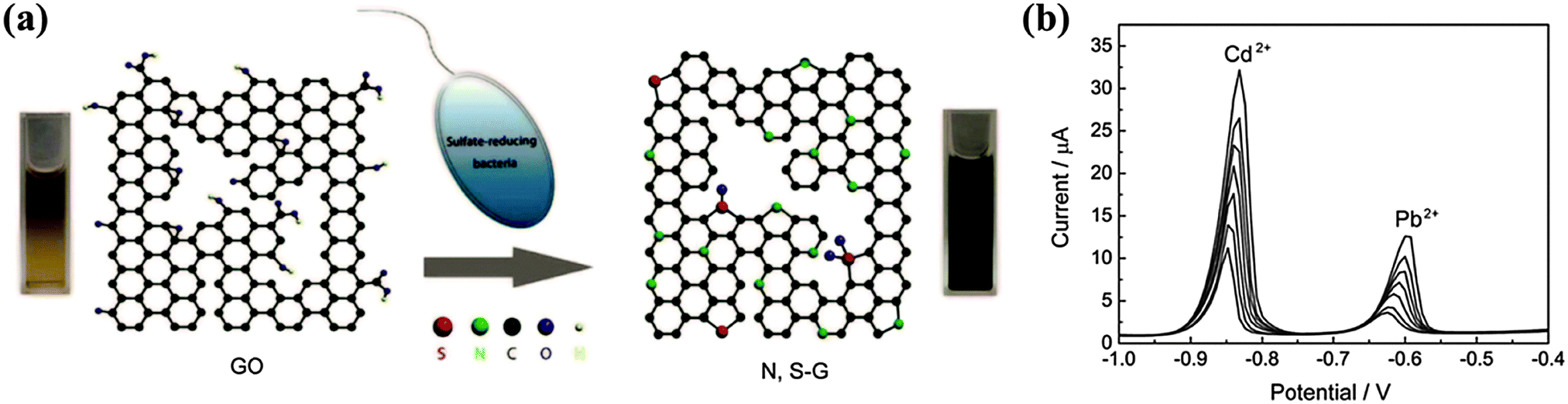 | ||
| Fig. 24 (a) Schematic illustration of the formation of N,S co-doped graphene by one-pot microbial reduction process. (b) Differential pulse anodic stripping voltammetry of the simultaneous analysis of Pb2+and Cd2+ with concentrations of 30, 24, 18, 15, 12 and 9 μg L−1. Adapted with permission from ref. 266. Copyright (2013) Nature Publishing Group. | ||
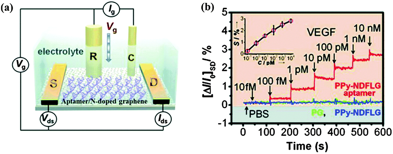 | ||
| Fig. 25 (a) Schematic diagram of a liquid-ion gated FET using aptamer-conjugated N-doped graphene (Ag/AgCl reference electrode, R; platinum counter electrode, C; source and drain electrodes, S and D). (b) Real-time responses and calibration curve (S in the inset indicates ΔI/I0) of aptasensor with various vascular endothelial growth factor concentrations. Adapted with permission from ref. 39. Copyright (2012) American Chemical Society. | ||
Heteroatom doping can create active sites for the strong adsorption of gas molecules, which, in turn, leads to a dramatic change of graphene conductance. It has been theoretically proven that various electronic sensors can be developed for gas sensing. Zhang et al. suggested that B-doped graphene can be used for the sensitive detection of NO2.269 Dai et al. showed that NO and NO2 can be electrically detected by B or S-doped graphene devices.184 Graphene with metal (e.g., Fe, Co) or Si dopants could be used for H2S sensing.270 However, for practical gas sensors, the possible inference from O2 molecules should be considered. It has been found that Si- and P-doped graphene yield the stable chemisorption of O2, whereas B- and N-doped graphene are inert to O2.271 The strong chemical reactivity of Si-doped graphene with O2 and NO2 was also reported by Zou et al.190
Despite proven potentials, the experimental demonstrations of doped graphene for gas sensing are rare till now. Using N,Si co-doped graphene for the electrical detection of NO2 was recently presented (Fig. 26a).272 N,Si co-doped graphene, synthesized by simply annealing GO in the presence of Si-containing IL, shows a resistance decrease while exposed to NO2 gas (∼26% reduction at 21 ppm and 8.8% at 1 ppm) (Fig. 26b). Contradictory to the expectation from the strong chemisorption of NO2 on Si-doped graphene,190 this sensor shows excellent reversibility. This discrepancy may be explained by the low abundance of Si dopants and the doping configurations different than those assumed in the simulation study.
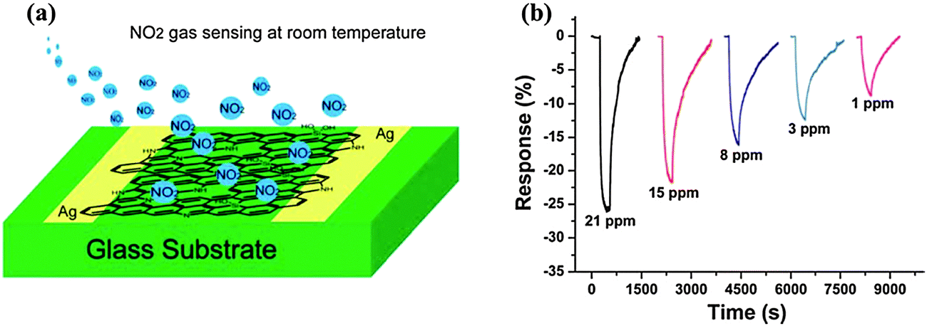 | ||
| Fig. 26 (a) NO2 sensor based on N,Si co-doped graphene and (b) its response to NO2 for different concentrations. Adapted with permission from ref. 272. Copyright (2013) Royal Society of Chemistry. | ||
Lv et al. experimentally demonstrated the first SERS sensor based on N-doped graphene.275 N-doped graphene (0.25 at%, two N atoms separated by one C atom in the same A sublattice as the dominant configuration) synthesized by atmospheric-pressure CVD was used to probe rhodamine B (RhB) molecules (Fig. 27). In comparison with pristine graphene, its N-doped counterpart gave a 10 times stronger signal at 1650 cm−1 for the fingerprints of RhB with additional vibration peaks at 1282 cm−1, 1531 cm−1 and 1567 cm−1 (Fig. 27c). The charge transfer (p-doping) by RhB underlies the detection.
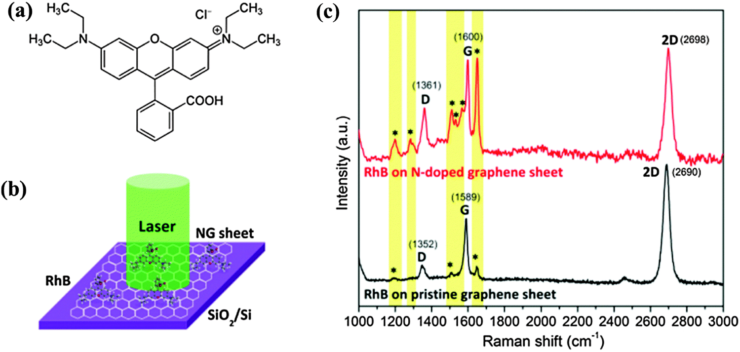 | ||
| Fig. 27 Enhanced Raman scattering effect of N-doped graphene sheets for probing RhB molecules. (a) Molecular structure of RhB. (b) Schematic illustration of experimental setup. RhB molecules are anchored onto the NG sheet/SiO2/Si substrate. The laser line is 514 nm. (c) Raman signals (*) of RhB molecules. Adapted with permission from ref. 275. Copyright (2012) Nature Publishing Group. | ||
4.6 Gas storage
Hydrogen is an ideal energy carrier with a non-polluting nature and high energy density. However, its storage is currently a huge technical hurdle for transportation and practical applications. Modifying graphene materials with metal nanoparticles (e.g. alkali and alkaline earth metals) can improve the gravimetric storage capacity via the polarization-induced interaction between metal and hydrogen atoms.276 However, decorated nanoparticles suffer from aggregation and poor stability. Heteroatom doping can assist nanoparticle dispersion and high coverage on graphene, as well as H2 adsorption. Parambhath et al. synthesized pyrrolic-N dominant graphene (7 at%) for H2 storage.277 In comparison with undoped graphene, it increased the H2 storage capabilities by 66% (0.88 wt%) at 25 °C and 2 MPa. A further 124% enhancement was achieved with an additional decoration of Pd nanoparticles. The highly dispersed and strongly bonded Pd nanoparticles promote H2 dissociation and the resulting hydrogen atom migration to the underneath of N-doped graphene. It has been theoretically predicted that H2 absorption on N-doped graphene can be further strengthened by the adsorbed Li atoms.278,279B-doping-induced graphene polarization and electron deficiency is also favorable for hydrogen adsorption, which is even more effective than graphitic-N doping.118,280 Theoretical calculations show a high H2 storage capacity (8.38 wt%) of Ca-decorated B-doped (12 at%) graphene.281 Further, the desirable interaction between H2 and B,Ca-decorated graphene makes H2 storage possible even at room temperature and ambient pressure.
Developing techniques to capture greenhouse gases (e.g., CO2) is critical to deal with global warming. Kim et al. reported a high gravimetric CO2 storage capacity (2.7 mmol g−1 at 298 K and 1 atm) of N-doped graphene, which is comparable to that of PANI-graphene composite at high pressure.282 The superior performance is attributable to the strong interaction between the N-dopants and CO2 molecules. It is also demonstrated that these N-doped graphene materials possess high recycling stability and selectivity over N2, CH4 and H2. Heteroatom-doped graphene could be used to capture other gases considering its high binding affinity with other gas molecules (e.g., NO, NO2, SO2).184
5 Summary and perspectives
As discussed in this article, heteroatom doping can endow graphene with various new electromagnetic, physicochemical, optical, and structural properties, depending on the dopants and doping configurations. This greatly extends the arsenal of graphene materials and their potential for a spectrum of applications. Different approaches have been developed for heteroatom doping. Doping type, level and configurations (hence, the properties of obtained materials) are critically determined by the chosen precursors, starting graphene material, reaction time, temperature, etc. Despite the tremendous progress made thus far, it is, however, still a current challenge to precisely control heteroatom doping. Based on both experimental and theoretical studies, we have comparably discussed the distinct effects induced by specific dopants, different bonding configurations of a given dopant, and synergistic actions between co-dopants. However, the current understanding on the properties of doped graphene materials is still far from complete and sometimes even contradictory because of the large and uncontrolled heterogeneity of the materials obtained from the current synthesis approaches.The emerging applications of doped graphene materials for energy storage, energy conversion, sensors, and gas storage have been surveyed in the present study. We envision that a better understanding on the doping mechanisms and doping properties based on both theoretical and experimental investigations, further development of controllable synthesis methods, and incorporation of new dopants will greatly extend the application scope of doped graphene materials. As different dopants, doping configurations and their relative ratios, and compositions of co-dopants confer graphene with distinct properties, the selection and engineering of these parameters should be application-specific. For example, multi-dopants with an optimal balance, which can simultaneously enhance charge polarization, spin density, and conductivity, are desired for ORR.
When graphene transforms from its native 2D structure to 1D (nanoribbons) or 0D (graphene quantum dots. GQD), dramatically altered or new properties arise due to quantum confinement and edge effects. Although not discussed here, we speculate that heteroatom doping on 1D and 0D graphene materials will open up new horizons in graphene research and applications. For example, it has been shown that the fluorescent properties of GQDs can be tailored by heteroatom doping for novel bio-imaging or optical sensing applications.283–286
Graphene research will continue to thrive because of the new opportunities provided by heteroatom doping. This article aims to provide useful clues for developing new and controllable synthesis methods and a better understanding of the properties of doped graphene materials. We also hope that it will inspire more exciting applications of this growing family of nanomaterials.
Acknowledgements
We thank the support from Ministry of Education of Singapore under an AcRF Tier 2 grant (MOE2011-T2-2-010, MOE2012-T2-2-049), the Agency for Science, Technology and Research (A*STAR) under a SERC Grant (102 170 0142), and NNSF of China (61328401).References
- A. K. Geim and K. S. Novoselov, Nat. Mater., 2007, 6, 183–191 CrossRef CAS PubMed.
- A. H. Castro Neto, F. Guinea, N. M. R. Peres, K. S. Novoselov and A. K. Geim, Rev. Mod. Phys., 2009, 81, 109–162 CrossRef CAS.
- D. Jariwala, V. K. Sangwan, L. J. Lauhon, T. J. Marks and M. C. Hersam, Chem. Soc. Rev., 2013, 42, 2824–2860 RSC.
- K. C. Yung, W. M. Wu, M. P. Pierpoint and F. V. Kusmartsev, Contemp. Phys., 2013, 54, 233–251 CrossRef CAS.
- N. Mahmood, C. Z. Zhang, H. Yin and Y. L. Hou, J. Mater. Chem. A, 2014, 2, 15–32 CAS.
- Y. Q. Sun, Q. O. Wu and G. Q. Shi, Energy Environ. Sci., 2011, 4, 1113–1132 CAS.
- J. Zhang, F. Zhao, Z. P. Zhang, N. Chen and L. T. Qu, Nanoscale, 2013, 5, 3112–3126 RSC.
- Y. X. Liu, X. C. Dong and P. Chen, Chem. Soc. Rev., 2012, 41, 2283–2307 RSC.
- L. Y. Feng, L. Wu and X. G. Qu, Adv. Mater., 2013, 25, 168–186 CrossRef CAS PubMed.
- K. Yang, Y. J. Li, X. F. Tan, R. Peng and Z. Liu, Small, 2013, 9, 1492–1503 CrossRef CAS PubMed.
- D. Zhan, J. X. Yan, L. F. Lai, Z. H. Ni, L. Liu and Z. X. Shen, Adv. Mater., 2012, 24, 4055–4069 CrossRef CAS PubMed.
- W. L. Wei and X. G. Qu, Small, 2012, 8, 2138–2151 CrossRef CAS PubMed.
- Y. W. Zhu, S. Murali, W. W. Cai, X. S. Li, J. W. Suk, J. R. Potts and R. S. Ruoff, Adv. Mater., 2010, 22, 3906–3924 CrossRef CAS PubMed.
- X. T. Zheng, A. Than, A. Ananthanaraya, D. H. Kim and P. Chen, ACS Nano, 2013, 7, 6278–6286 CrossRef CAS PubMed.
- J. H. Shen, Y. H. Zhu, X. L. Yang and C. Z. Li, Chem. Commun., 2012, 48, 3686–3699 RSC.
- L. L. Li, G. H. Wu, G. H. Yang, J. Peng, J. W. Zhao and J. J. Zhu, Nanoscale, 2013, 5, 4015–4039 RSC.
- A. Ananthanarayanan, X. W. Wang, P. Routh, B. Sana, S. Lim, D. H. Kim, K. H. Lim, J. Li and P. Chen, Adv. Funct. Mater., 2014, 24, 3021–3026 CrossRef CAS.
- S. Dutta and S. K. Pati, J. Mater. Chem., 2010, 20, 8207–8223 RSC.
- X. Dong, Q. Long, J. Wang, M. B. Chan-Park, Y. Huang, W. Huang and P. Chen, Nanoscale, 2011, 3, 5156–5160 RSC.
- C. Li and G. Q. Shi, Nanoscale, 2012, 4, 5549–5563 RSC.
- X. C. Dong, H. Xu, X. W. Wang, Y. X. Huang, M. B. Chan-Park, H. Zhang, L. H. Wang, W. Huang and P. Chen, ACS Nano, 2012, 6, 3206–3213 CrossRef CAS PubMed.
- Y. C. Yong, X. C. Dong, M. B. Chan-Park, H. Song and P. Chen, ACS Nano, 2012, 6, 2394–2400 CrossRef CAS PubMed.
- X. C. Dong, D. L. Fu, W. J. Fang, Y. M. Shi, P. Chen and L. J. Li, Small, 2009, 5, 1422–1426 CrossRef CAS PubMed.
- X. C. Dong, Q. Long, A. Wei, W. J. Zhang, L. J. Li, P. Chen and W. Huang, Carbon, 2012, 50, 1517–1522 CrossRef CAS.
- V. Georgakilas, M. Otyepka, A. B. Bourlinos, V. Chandra, N. Kim, K. C. Kemp, P. Hobza, R. Zboril and K. S. Kim, Chem. Rev., 2012, 112, 6156–6214 CrossRef CAS PubMed.
- R. T. Lv and M. Terrones, Mater. Lett., 2012, 78, 209–218 CrossRef CAS.
- U. N. Maiti, W. J. Lee, J. M. Lee, Y. Oh, J. Y. Kim, J. E. Kim, J. Shim, T. H. Han and S. O. Kim, Adv. Mater., 2014, 26, 40–67 CrossRef CAS PubMed.
- X. K. Kong, C. L. Chen and Q. W. Chen, Chem. Soc. Rev., 2014, 43, 2841–2857 RSC.
- D. W. Wang and D. S. Su, Energy Environ. Sci., 2014, 7, 576–591 CAS.
- C. K. Chang, S. Kataria, C. C. Kuo, A. Ganguly, B. Y. Wang, J. Y. Hwang, K. J. Huang, W. H. Yang, S. B. Wang, C. H. Chuang, M. Chen, C. I. Huang, W. F. Pong, K. J. Song, S. J. Chang, J. H. Guo, Y. Tai, M. Tsujimoto, S. Isoda, C. W. Chen, L. C. Chen and K. H. Chen, ACS Nano, 2013, 7, 1333–1341 CrossRef CAS PubMed.
- T. R. Wu, H. L. Shen, L. Sun, B. Cheng, B. Liu and J. C. Shen, New J. Chem., 2012, 36, 1385–1391 RSC.
- X. Li, L. L. Fan, Z. Li, K. L. Wang, M. L. Zhong, J. Q. Wei, D. H. Wu and H. W. Zhu, Adv. Energy Mater., 2012, 2, 425–429 CrossRef CAS.
- L. Ci, L. Song, C. H. Jin, D. Jariwala, D. X. Wu, Y. J. Li, A. Srivastava, Z. F. Wang, K. Storr, L. Balicas, F. Liu and P. M. Ajayan, Nat. Mater., 2010, 9, 430–435 CrossRef CAS PubMed.
- G. Bepete, D. Voiry, M. Chhowalla, Z. Chiguvare and N. J. Coville, Nanoscale, 2013, 5, 6552–6557 RSC.
- Y. H. Xue, D. S. Yu, L. M. Dai, R. G. Wang, D. Q. Li, A. Roy, F. Lu, H. Chen, Y. Liu and J. Qu, Phys. Chem. Chem. Phys., 2013, 15, 12220–12226 RSC.
- H. Wang, Y. Zhou, D. Wu, L. Liao, S. L. Zhao, H. L. Peng and Z. F. Liu, Small, 2013, 9, 1316–1320 CrossRef CAS PubMed.
- A. L. M. Reddy, A. Srivastava, S. R. Gowda, H. Gullapalli, M. Dubey and P. M. Ajayan, ACS Nano, 2010, 4, 6337–6342 CrossRef CAS PubMed.
- Z. Jin, J. Yao, C. Kittrell and J. M. Tour, ACS Nano, 2011, 5, 4112–4117 CrossRef CAS PubMed.
- O. S. Kwon, S. J. Park, J. Y. Hong, A. R. Han, J. S. Lee, J. S. Lee, J. H. Oh and J. Jang, ACS Nano, 2012, 6, 1486–1493 CrossRef CAS PubMed.
- Z. Z. Sun, Z. Yan, J. Yao, E. Beitler, Y. Zhu and J. M. Tour, Nature, 2010, 468, 549–552 CrossRef CAS PubMed.
- Y. W. Zhang, J. Ge, L. Wang, D. H. Wang, F. Ding, X. M. Tao and W. Chen, Sci. Rep., 2013, 3, 2771 Search PubMed.
- D. C. Wei, Y. Q. Liu, Y. Wang, H. L. Zhang, L. P. Huang and G. Yu, Nano Lett., 2009, 9, 1752–1758 CrossRef CAS PubMed.
- L. T. Qu, Y. Liu, J. B. Baek and L. M. Dai, ACS Nano, 2010, 4, 1321–1326 CrossRef CAS PubMed.
- H. Gao, Z. Liu, L. Song, W. H. Guo, W. Gao, L. J. Ci, A. Rao, W. J. Quan, R. Vajtai and P. M. Ajayan, Nanotechnology, 2012, 23, 275605 CrossRef PubMed.
- J. X. Xu, G. F. Dong, C. H. Jin, M. H. Huang and L. H. Guan, ChemSusChem, 2013, 6, 493–499 CrossRef CAS PubMed.
- G. Kalita, K. Wakita, M. Takahashi and M. Umeno, J. Mater. Chem., 2011, 21, 15209–15213 RSC.
- I. Y. Jeon, Y. R. Shin, G. J. Sohn, H. J. Choi, S. Y. Bae, J. Mahmood, S. M. Jung, J. M. Seo, M. J. Kim, D. W. Chang, L. M. Dai and J. B. Baek, Proc. Natl. Acad. Sci. U. S. A., 2012, 109, 5588–5593 CrossRef CAS PubMed.
- L. Yan, M. M. Lin, C. Zeng, Z. Chen, S. Zhang, X. M. Zhao, A. G. Wu, Y. P. Wang, L. M. Dai, J. Qu, M. M. Guo and Y. Liu, J. Mater. Chem., 2012, 22, 8367–8371 RSC.
- I. Y. Jeon, H. J. Choi, M. J. Ju, I. T. Choi, K. Lim, J. Ko, H. K. Kim, J. C. Kim, J. J. Lee, D. Shin, S. M. Jung, J. M. Seo, M. J. Kim, N. Park, L. Dai and J. B. Baek, Sci. Rep., 2013, 3, 2260 Search PubMed.
- K. Brenner and R. Murali, Appl. Phys. Lett., 2011, 98, 113115 CrossRef.
- I. Y. Jeon, H. J. Choi, M. Choi, J. M. Seo, S. M. Jung, M. J. Kim, S. Zhang, L. P. Zhang, Z. H. Xia, L. M. Dai, N. Park and J. B. Baek, Sci. Rep., 2013, 3, 1810 Search PubMed.
- I. Y. Jeon, H. J. Choi, S. M. Jung, J. M. Seo, M. J. Kim, L. M. Dai and J. B. Baek, J. Am. Chem. Soc., 2013, 135, 1386–1393 CrossRef CAS PubMed.
- I. Y. Jeon, S. Zhang, L. P. Zhang, H. J. Choi, J. M. Seo, Z. H. Xia, L. M. Dai and J. B. Baek, Adv. Mater., 2013, 25, 6138–6145 CrossRef CAS PubMed.
- X. J. Lu, J. J. Wu, T. Q. Lin, D. Y. Wan, F. Q. Huang, X. M. Xie and M. H. Jiang, J. Mater. Chem., 2011, 21, 10685–10689 RSC.
- D. H. Deng, X. L. Pan, L. A. Yu, Y. Cui, Y. P. Jiang, J. Qi, W. X. Li, Q. A. Fu, X. C. Ma, Q. K. Xue, G. Q. Sun and X. H. Bao, Chem. Mater., 2011, 23, 1188–1193 CrossRef CAS.
- D. Geng, Y. Hu, Y. Li, R. Li and X. Sun, Electrochem. Commun., 2012, 22, 65–68 CrossRef CAS.
- T. Q. Lin, F. Q. Huang, J. Liang and Y. X. Wang, Energy Environ. Sci., 2011, 4, 862–865 Search PubMed.
- H. L. Peng, Z. Y. Mo, S. J. Liao, H. G. Liang, L. J. Yang, F. Luo, H. Y. Song, Y. L. Zhong and B. Q. Zhang, Sci. Rep., 2013, 3, 1765 Search PubMed.
- Z. S. Wu, W. C. Ren, L. Xu, F. Li and H. M. Cheng, ACS Nano, 2011, 5, 5463–5471 CrossRef CAS PubMed.
- Z. C. Zuo, Z. Q. Jiang and A. Manthiram, J. Mater. Chem. A, 2013, 1, 13476–13483 CAS.
- X. L. Li, H. L. Wang, J. T. Robinson, H. Sanchez, G. Diankov and H. J. Dai, J. Am. Chem. Soc., 2009, 131, 15939–15944 CrossRef CAS PubMed.
- L. S. Zhang, X. Q. Liang, W. G. Song and Z. Y. Wu, Phys. Chem. Chem. Phys., 2010, 12, 12055–12059 RSC.
- G. H. Jun, S. H. Jin, B. Lee, B. H. Kim, W. S. Chae, S. H. Hong and S. Jeon, Energy Environ. Sci., 2013, 6, 3000–3006 CAS.
- B. Xiong, Y. K. Zhou, Y. Y. Zhao, J. Wang, X. Chen, R. O'Hayre and Z. P. Shao, Carbon, 2013, 52, 181–192 CrossRef CAS.
- D. S. Geng, Y. Chen, Y. G. Chen, Y. L. Li, R. Y. Li, X. L. Sun, S. Y. Ye and S. Knights, Energy Environ. Sci., 2011, 4, 760–764 CAS.
- E. Yoo, J. Nakamura and H. S. Zhou, Energy Environ. Sci., 2012, 5, 6928–6932 CAS.
- T. V. Khai, H. G. Na, D. S. Kwak, Y. J. Kwon, H. Ham, K. B. Shim and H. W. Kim, J. Mater. Chem., 2012, 22, 17992–18003 RSC.
- H. B. Wang, C. J. Zhang, Z. H. Liu, L. Wang, P. X. Han, H. X. Xu, K. J. Zhang, S. M. Dong, J. H. Yao and G. L. Cui, J. Mater. Chem., 2011, 21, 5430–5434 RSC.
- S. Y. Wang, L. P. Zhang, Z. H. Xia, A. Roy, D. W. Chang, J. B. Baek and L. M. Dai, Angew. Chem., Int. Ed., 2012, 51, 4209–4212 CrossRef CAS PubMed.
- L. F. Lai, J. R. Potts, D. Zhan, L. Wang, C. K. Poh, C. H. Tang, H. Gong, Z. X. Shen, L. Y. Jianyi and R. S. Ruoff, Energy Environ. Sci., 2012, 5, 7936–7942 CAS.
- Z. H. Sheng, L. Shao, J. J. Chen, W. J. Bao, F. B. Wang and X. H. Xia, ACS Nano, 2011, 5, 4350–4358 CrossRef CAS PubMed.
- Z. Y. Lin, G. H. Waller, Y. Liu, M. L. Liu and C. P. Wong, Carbon, 2013, 53, 130–136 CrossRef CAS.
- S. C. Hou, X. Cai, H. W. Wu, X. Yu, M. Peng, K. Yan and D. C. Zou, Energy Environ. Sci., 2013, 6, 3356–3362 CAS.
- C. H. Choi, M. W. Chung, S. H. Park and S. I. Woo, RSC Adv., 2013, 3, 4246–4253 RSC.
- J. Y. Liu, H. Y. Chang, Q. D. Truong and Y. C. Ling, J. Mater. Chem. C, 2013, 1, 1713–1716 RSC.
- R. Li, Z. Wei, X. Gou and W. Xu, RSC Adv., 2013, 3, 9978–9984 RSC.
- S. B. Yang, L. J. Zhi, K. Tang, X. L. Feng, J. Maier and K. Mullen, Adv. Funct. Mater., 2012, 22, 3634–3640 CrossRef CAS.
- H. L. Poh, P. Simek, Z. Sofer and M. Pumera, ACS Nano, 2013, 7, 5262–5272 CrossRef CAS PubMed.
- M. Seredych, J. C. Idrobo and T. J. Bandosz, J. Mater. Chem. A, 2013, 1, 7059–7067 CAS.
- C. H. Choi, M. W. Chung, Y. J. Jun and S. I. Woo, RSC Adv., 2013, 3, 12417–12422 RSC.
- R. Y. Wang, D. C. Higgins, M. A. Hoque, D. Lee, F. Hassan and Z. W. Chen, Sci. Rep., 2013, 3, 2431 Search PubMed.
- Z. Yang, Z. Yao, G. F. Li, G. Y. Fang, H. G. Nie, Z. Liu, X. M. Zhou, X. Chen and S. M. Huang, ACS Nano, 2012, 6, 205–211 CrossRef CAS PubMed.
- J. Liang, Y. Jiao, M. Jaroniec and S. Z. Qiao, Angew. Chem., Int. Ed., 2012, 51, 11496–11500 CrossRef CAS PubMed.
- H. L. Poh, P. Simek, Z. Sofer and M. Pumera, Chem. – Eur. J., 2013, 19, 2655–2662 CrossRef CAS PubMed.
- Z. Yao, H. G. Nie, Z. Yang, X. M. Zhou, Z. Liu and S. M. Huang, Chem. Commun., 2012, 48, 1027–1029 RSC.
- P. Wu, Z. W. Cai, Y. Gao, H. Zhang and C. X. Cai, Chem. Commun., 2011, 47, 11327–11329 RSC.
- P. Wu, Y. D. Qian, P. Du, H. Zhang and C. X. Cai, J. Mater. Chem., 2012, 22, 6402–6412 RSC.
- Y. H. S. Park, J. O. Hwang, E.-S. Lee, L. B. Casabianca, W. Cai, J. R. Potts, H.-W. Ha, S. Chen, J. Oh, S. O. Kim, Y.-H. Kim, Y. Ishii and R. S. Ruoff, Nat. Commun., 2012, 3, 1–8 Search PubMed.
- D. H. Long, W. Li, L. C. Ling, J. Miyawaki, I. Mochida and S. H. Yoon, Langmuir, 2010, 26, 16096–16102 CrossRef CAS PubMed.
- B. Jiang, C. Tian, L. Wang, L. Sun, C. Chen, X. Nong, Y. Qiao and H. Fu, Appl. Surf. Sci., 2012, 258, 3438–3443 CrossRef CAS.
- L. Sun, L. Wang, C. G. Tian, T. X. Tan, Y. Xie, K. Y. Shi, M. T. Li and H. G. Fu, RSC Adv., 2012, 2, 4498–4506 RSC.
- J. W. Lee, J. M. Ko and J. D. Kim, Electrochim. Acta, 2012, 85, 459–466 CrossRef CAS.
- Y. J. Zhang, K. Fugane, T. Mori, L. Niu and J. H. Ye, J. Mater. Chem., 2012, 22, 6575–6580 RSC.
- Y. Z. Chang, G. Y. Han, J. P. Yuan, D. Y. Fu, F. F. Liu and S. D. A. Li, J. Power Sources, 2013, 238, 492–500 CrossRef CAS.
- Y. Z. Su, Y. Zhang, X. D. Zhuang, S. Li, D. Q. Wu, F. Zhang and X. L. Feng, Carbon, 2013, 62, 296–301 CrossRef CAS.
- R. Ballesteros-Garrido, H. G. Baldovi, M. Latorre-Sanchez, M. Alvaro and H. Garcia, J. Mater. Chem. A, 2013, 1, 11728–11734 CAS.
- P. W. Gong, Z. F. Wang, J. Q. Wang, H. G. Wang, Z. P. Li, Z. J. Fan, Y. Xu, X. X. Han and S. R. Yang, J. Mater. Chem., 2012, 22, 16950–16956 RSC.
- H. X. Chang, J. S. Cheng, X. Q. Liu, J. F. Gao, M. J. Li, J. H. Li, X. M. Tao, F. Ding and Z. J. Zheng, Chem. – Eur. J., 2011, 17, 8896–8903 CrossRef CAS PubMed.
- J. Zheng, H. T. Liu, B. Wu, C. A. Di, Y. L. Guo, T. Wu, G. Yu, Y. Q. Liu and D. B. Zhu, Sci. Rep., 2012, 2, 662 Search PubMed.
- H. L. Guo, P. Su, X. F. Kang and S. K. Ning, J. Mater. Chem. A, 2013, 1, 2248–2255 CAS.
- Z. S. Wu, A. Winter, L. Chen, Y. Sun, A. Turchanin, X. L. Feng and K. Mullen, Adv. Mater., 2012, 24, 5130–5135 CrossRef CAS PubMed.
- Y. Y. Zhao, Y. K. Zhou, B. Xiong, J. Wang, X. Chen, R. O'Hayre and Z. P. Shao, J. Solid State Electrochem., 2013, 17, 1089–1098 CrossRef CAS.
- Z. S. Wu, S. B. Yang, Y. Sun, K. Parvez, X. L. Feng and K. Mullen, J. Am. Chem. Soc., 2012, 134, 9082–9085 CrossRef CAS PubMed.
- S. H. Yang, X. F. Song, P. Zhang and L. Gao, ACS Appl. Mater. Interfaces, 2013, 5, 3317–3322 CAS.
- R. F. Nie, J. J. Shi, W. C. Du, W. S. Ning, Z. Y. Hou and F. S. Xiao, J. Mater. Chem. A, 2013, 1, 9037–9045 CAS.
- C. Nethravathi, C. R. Rajamathi, M. Rajamathi, U. K. Gautam, X. Wang, D. Golberg and Y. Bando, ACS Appl. Mater. Interfaces, 2013, 5, 2708–2714 CAS.
- P. H. Shi, R. J. Su, F. Z. Wan, M. C. Zhu, D. X. Li and S. H. Xu, Appl. Catal., B, 2012, 123, 265–272 CrossRef.
- H. M. Jeong, J. W. Lee, W. H. Shin, Y. J. Choi, H. J. Shin, J. K. Kang and J. W. Choi, Nano Lett., 2011, 11, 2472–2477 CrossRef CAS PubMed.
- Y. Wang, Y. Shao, D. W. Matson, J. Li and Y. Lin, ACS Nano, 2010, 4, 1790–1798 CrossRef CAS PubMed.
- S. Gulbagh, D. S. Sutar, V. D. Botcha, K. N. Pavan, S. S. Talwar, R. S. Srinivasa and S. S. Major, Nanotechnology, 2013, 24, 355704 CrossRef PubMed.
- J. Wu, L. M. Xie, Y. G. Li, H. L. Wang, Y. J. Ouyang, J. Guo and H. J. Dai, J. Am. Chem. Soc., 2011, 133, 19668–19671 CrossRef CAS PubMed.
- X. Zhang, A. Hsu, H. Wang, Y. Song, J. Kong, M. S. Dresselhaus and T. Palacios, ACS Nano, 2013, 7, 7262–7270 CrossRef CAS PubMed.
- B. Li, L. Zhou, D. Wu, H. L. Peng, K. Yan, Y. Zhou and Z. F. Liu, ACS Nano, 2011, 5, 5957–5961 CrossRef CAS PubMed.
- N. Li, Z. Y. Wang, K. K. Zhao, Z. J. Shi, Z. N. Gu and S. K. Xu, Carbon, 2010, 48, 255–259 CrossRef CAS.
- L. S. Panchakarla, K. S. Subrahmanyam, S. K. Saha, A. Govindaraj, H. R. Krishnamurthy, U. V. Waghmare and C. N. R. Rao, Adv. Mater., 2009, 21, 4726–4730 CAS.
- B. S. Shen, J. T. Chen, X. B. Yan and Q. J. Xue, RSC Adv., 2012, 2, 6761–6764 RSC.
- P. Rani and V. K. Jindal, RSC Adv., 2013, 3, 802–812 RSC.
- R. H. Miwa, T. B. Martins and A. Fazzio, Nanotechnology, 2008, 19, 155708 CrossRef CAS PubMed.
- R. Faccio, L. Fernandez-Werner, H. Pardo, C. Goyenola, O. N. Ventura and A. W. Mombru, J. Phys. Chem. C, 2010, 114, 18961–18971 CAS.
- K. Z.M. Magdalena Woínska and J.-A. Majewski, Phys. Status Solidi C, 2013, 10, 1167–1171 CrossRef.
- L. S. Panchokarla, K. S. Subrahmanyam, S. K. Saha, A. Govindaraj, H. R. Krishnamurthy, U. V. Waghmare and C. N. R. Rao, Adv. Mater., 2009, 21, 4726–4730 Search PubMed.
- B. Mortazavi and S. Ahzi, Solid State Commun., 2012, 152, 1503–1507 CrossRef CAS.
- B. Zheng, P. Hermet and L. Henrard, ACS Nano, 2010, 4, 4165–4173 CrossRef CAS PubMed.
- Q. Q. Zhu, J. H. Yu, W. S. Zhang, H. Z. Dong and L. F. Dong, J. Renewable Sustainable Energy, 2013, 5, 021408 CrossRef.
- S. Mukherjee and T. P. Kaloni, J. Nanopart. Res., 2012, 14, 1059 CrossRef.
- A. Lherbier, X. Blase, Y. M. Niquet, F. Triozon and S. Roche, Phys. Rev. Lett., 2008, 101, 036808 CrossRef PubMed.
- H. Mousavi and R. Moradian, Solid State Sci., 2011, 13, 1459–1464 CrossRef CAS.
- S. O. Guillaume, B. Zheng, J. C. Charlier and L. Henrard, Phys. Rev. B: Condens. Matter Mater. Phys., 2012, 85, 035444 CrossRef.
- D. Usachov, O. Vilkov, A. Gruneis, D. Haberer, A. Fedorov, V. K. Adamchuk, A. B. Preobrajenski, P. Dudin, A. Barinov, M. Oehzelt, C. Laubschat and D. V. Vyalikh, Nano Lett., 2011, 11, 5401–5407 CrossRef CAS PubMed.
- M. M. Yang, L. Zhou, J. Y. Wang, Z. F. Liu and Z. R. Liu, J. Phys. Chem. C, 2012, 116, 844–850 CAS.
- Z. F. Hou, X. L. Wang, T. Ikeda, K. Terakura, M. Oshima and M. Kakimoto, Phys. Rev. B: Condens. Matter Mater. Phys., 2013, 87, 165401 CrossRef.
- Z. F. Hou, X. L. Wang, T. Ikeda, K. Terakura, M. Oshima, M. Kakimoto and S. Miyata, Phys. Rev. B: Condens. Matter Mater. Phys., 2012, 85, 165439 CrossRef.
- P. Wu, P. Du, H. Zhang and C. Cai, Phys. Chem. Chem. Phys., 2013, 15, 6920–6928 RSC.
- A. Lherbier, A. R. Botello-Mendez and J. C. Charlier, Nano Lett., 2013, 13, 1446–1450 CAS.
- D. Wei, Y. Liu, Y. Wang, H. Zhang, L. Huang and G. Yu, Nano Lett., 2009, 9, 1752–1758 CrossRef CAS PubMed.
- S. Jalili and R. Vaziri, Mol. Phys., 2011, 109, 687–694 CrossRef CAS.
- T. Schiros, D. Nordlund, L. Palova, D. Prezzi, L. Y. Zhao, K. S. Kim, U. Wurstbauer, C. Gutierrez, D. Delongchamp, C. Jaye, D. Fischer, H. Ogasawara, L. G. M. Pettersson, D. R. Reichman, P. Kim, M. S. Hybertsen and A. N. Pasupathy, Nano Lett., 2012, 12, 4025–4031 CrossRef CAS PubMed.
- Y. F. Lu, S. T. Lo, J. C. Lin, W. J. Zhang, J. Y. Lu, F. H. Liu, C. M. Tseng, Y. H. Lee, C. T. Liang and L. J. Li, ACS Nano, 2013, 7, 6522–6532 CrossRef CAS PubMed.
- F. Cervantes-Sodi, G. Csanyi, S. Piscanec and A. C. Ferrari, Phys. Rev. B: Condens. Matter Mater. Phys., 2008, 77, 165427 CrossRef.
- E. Velez-Fort, C. Mathieu, E. Pallecchi, M. Pigneur, M. G. Silly, R. Belkhou, M. Marangolo, A. Shukla, F. Sirotti and A. Ouerghi, ACS Nano, 2012, 6, 10893–10900 CAS.
- J. O. Hwang, J. S. Park, D. S. Choi, J. Y. Kim, S. H. Lee, K. E. Lee, Y. H. Kim, M. H. Song, S. Yoo and S. O. Kim, ACS Nano, 2012, 6, 159–167 CrossRef CAS PubMed.
- Z. Luo, S. Lim, Z. Tian, J. Shang, L. Lai, B. MacDonald, C. Fu, Z. Shen, T. Yu and J. Lin, J. Mater. Chem., 2011, 21, 8038–8044 RSC.
- Y. Liu, Q. Feng, N. J. Tang, X. G. Wan, F. C. Liu, L. Y. Lv and Y. W. Du, Carbon, 2013, 60, 549–551 CrossRef CAS.
- Y. Li, Z. Zhou, P. Shen and Z. Chen, ACS Nano, 2009, 3, 1952–1958 CrossRef CAS PubMed.
- J. W. Chiou, S. C. Ray, S. I. Peng, C. H. Chuang, B. Y. Wang, H. M. Tsai, C. W. Pao, H. J. Lin, Y. C. Shao, Y. F. Wang, S. C. Chen, W. F. Pong, Y. C. Yeh, C. W. Chen, L. C. Chen, K. H. Chen, M. H. Tsai, A. Kumar, A. Ganguly, P. Papakonstantinou, H. Yamane, N. Kosugi, T. Regier, L. Liu and T. K. Sham, J. Phys. Chem. C, 2012, 116, 16251–16258 CAS.
- T. Van Khai, H. G. Na, D. S. Kwak, Y. J. Kwon, H. Ham, K. B. Shim and H. W. Kim, J. Mater. Chem., 2012, 22, 17992–18003 RSC.
- M. Li, Z. Wu, W. Ren, H. Cheng, N. Tang, W. Wu, W. Zhong and Y. Du, Carbon, 2012, 50, 5286–5291 CrossRef CAS.
- H.-m. Wang, H.-x. Wang, Y. Chen, Y.-j. Liu, J.-x. Zhao, Q.-h. Cai and X.-z. Wang, Appl. Surf. Sci., 2013, 273, 302–309 CrossRef CAS.
- Z.-W. Liu, F. Peng, H.-J. Wang, H. Yu, W.-X. Zheng and J. Yang, Angew. Chem., Int. Ed., 2011, 50, 3257–3261 CrossRef PubMed.
- T. Schiros, D. Nordlund, L. Palova, D. Prezzi, L. Y. Zhao, K. S. Kim, U. Wurstbauer, C. Gutierrez, D. Delongchamp, C. Jaye, D. Fischer, H. Ogasawara, L. G. M. Pettersson, D. R. Reichman, P. Kim, M. S. Hybertsen and A. N. Pasupathy, Nano Lett., 2012, 12, 4025–4031 CrossRef CAS PubMed.
- S. Some, J. Kim, K. Lee, A. Kulkarni, Y. Yoon, S. Lee, T. Kim and H. Lee, Adv. Mater., 2012, 24, 5481–5486 CrossRef CAS PubMed.
- P. A. Denis, Comput. Mater. Sci., 2013, 67, 203–206 CrossRef CAS.
- J. Y. Dai and J. M. Yuan, J. Phys.: Condens. Matter, 2010, 22, 225501 CrossRef PubMed.
- K. A. Mkhoyan, A. W. Contryman, J. Silcox, D. A. Stewart, G. Eda, C. Mattevi, S. Miller and M. Chhowalla, Nano Lett., 2009, 9, 1058–1063 CrossRef CAS PubMed.
- D. W. Boukhvalov and M. I. Katsnelson, J. Am. Chem. Soc., 2008, 130, 10697–10701 CrossRef CAS PubMed.
- T. Szabo, O. Berkesi, P. Forgo, K. Josepovits, Y. Sanakis, D. Petridis and I. Dekany, Chem. Mater., 2006, 18, 2740–2749 CrossRef CAS.
- I. Jung, D. A. Dikin, R. D. Piner and R. S. Ruoff, Nano Lett., 2008, 8, 4283–4287 CrossRef CAS PubMed.
- Z. Xu, Y. Bando, L. Liu, W. L. Wang, X. D. Bai and D. Golberg, ACS Nano, 2011, 5, 4401–4406 CrossRef CAS PubMed.
- S. Kim, S. Zhou, Y. K. Hu, M. Acik, Y. J. Chabal, C. Berger, W. de Heer, A. Bongiorno and E. Riedo, Nat. Mater., 2012, 11, 544–549 CrossRef CAS PubMed.
- P. V. Kumar, M. Bernardi and J. C. Grossman, ACS Nano, 2013, 7, 1638–1645 CrossRef CAS PubMed.
- H. P. Jia, D. R. Dreyer and C. W. Bielawski, Tetrahedron, 2011, 67, 4431–4434 CrossRef CAS.
- D. S. Su, J. Zhang, B. Frank, A. Thomas, X. C. Wang, J. Paraknowitsch and R. Schlogl, ChemSusChem, 2010, 3, 169–180 CrossRef CAS PubMed.
- D. R. Dreyer, H. P. Jia and C. W. Bielawski, Angew. Chem., Int. Ed., 2010, 49, 6813–6816 CAS.
- D. R. Dreyer, S. Park, C. W. Bielawski and R. S. Ruoff, Chem. Soc. Rev., 2010, 39, 228–240 RSC.
- C. L. Su and K. P. Loh, Acc. Chem. Res., 2013, 46, 2275–2285 CrossRef CAS PubMed.
- P. A. Denis, Chem. Phys. Lett., 2010, 492, 251–257 CrossRef CAS.
- P. A. Denis, R. Faccio and A. W. Mombru, ChemPhysChem, 2009, 10, 715–722 CrossRef CAS PubMed.
- S. Glenis, A. J. Nelson and M. M. Labes, J. Appl. Phys., 1999, 86, 4464–4466 CrossRef CAS.
- R. Zboril, F. Karlicky, A. B. Bourlinos, T. A. Steriotis, A. K. Stubos, V. Georgakilas, K. Safarova, D. Jancik, C. Trapalis and M. Otyepka, Small, 2010, 6, 2885–2891 CrossRef CAS PubMed.
- M. A. Ribas, A. K. Singh, P. B. Sorokin and B. I. Yakobson, Nano Res., 2011, 4, 143–152 CrossRef CAS.
- J. T. Robinson, J. S. Burgess, C. E. Junkermeier, S. C. Badescu, T. L. Reinecke, F. K. Perkins, M. K. Zalalutdniov, J. W. Baldwin, J. C. Culbertson, P. E. Sheehan and E. S. Snow, Nano Lett., 2010, 10, 3001–3005 CrossRef CAS PubMed.
- R. R. Nair, W. C. Ren, R. Jalil, I. Riaz, V. G. Kravets, L. Britnell, P. Blake, F. Schedin, A. S. Mayorov, S. J. Yuan, M. I. Katsnelson, H. M. Cheng, W. Strupinski, L. G. Bulusheva, A. V. Okotrub, I. V. Grigorieva, A. N. Grigorenko, K. S. Novoselov and A. K. Geim, Small, 2010, 6, 2877–2884 CrossRef CAS PubMed.
- K. J. Jeon, Z. Lee, E. Pollak, L. Moreschini, A. Bostwick, C. M. Park, R. Mendelsberg, V. Radmilovic, R. Kostecki, T. J. Richardson and E. Rotenberg, ACS Nano, 2011, 5, 1042–1046 CrossRef CAS PubMed.
- P. V. C. Medeiros, A. J. S. Mascarenhas, F. D. Mota and C. M. C. de Castilho, Nanotechnology, 2010, 21, 485701 CrossRef PubMed.
- M. Klintenberg, S. Lebegue, M. I. Katsnelson and O. Eriksson, Phys. Rev. B: Condens. Matter Mater. Phys., 2010, 81, 085433 CrossRef.
- H. Sahin and S. Ciraci, J. Phys. Chem. C, 2012, 116, 24075–24083 CAS.
- A. Yaya, C. P. Ewels, I. Suarez-Martinez, P. Wagner, S. Lefrant, A. Okotrub, L. Bulusheva and P. R. Briddon, Phys. Rev. B: Condens. Matter Mater. Phys., 2011, 83, 045411 CrossRef.
- R. Balog, B. Jorgensen, L. Nilsson, M. Andersen, E. Rienks, M. Bianchi, M. Fanetti, E. Laegsgaard, A. Baraldi, S. Lizzit, Z. Sljivancanin, F. Besenbacher, B. Hammer, T. G. Pedersen, P. Hofmann and L. Hornekaer, Nat. Mater., 2010, 9, 315–319 CrossRef CAS PubMed.
- D. C. Elias, R. R. Nair, T. M. G. Mohiuddin, S. V. Morozov, P. Blake, M. P. Halsall, A. C. Ferrari, D. W. Boukhvalov, M. I. Katsnelson, A. K. Geim and K. S. Novoselov, Science, 2009, 323, 610–613 CrossRef CAS PubMed.
- M. Pumera and C. H. A. Wong, Chem. Soc. Rev., 2013, 42, 5987–5995 RSC.
- S. C. Ray, N. Soin, T. Makgato, C. H. Chuang, W. F. Pong, S. S. Roy, S. K. Ghosh, A. M. Strydom and J. A. McLaughlin, Sci. Rep., 2014, 4, 3862 Search PubMed.
- R. Jayasingha, A. Sherehiy, S. Y. Wu and G. U. Sumanasekera, Nano Lett., 2013, 13, 5098–5105 CrossRef CAS PubMed.
- Y. Lee, S. Lee, Y. Hwang and Y. C. Chung, Appl. Surf. Sci., 2014, 289, 445–449 CrossRef CAS.
- J. Y. Dai, J. M. Yuan and P. Giannozzi, Appl. Phys. Lett., 2009, 95, 232105 CrossRef.
- Z. M. Ao, J. Yang, S. Li and Q. Jiang, Chem. Phys. Lett., 2008, 461, 276–279 CrossRef CAS.
- J. X. Zhao, Y. Chen and H. G. Fu, Theor. Chem. Acc., 2012, 131, 1242 CrossRef.
- Y. Chen, X. C. Yang, Y. J. Liu, J. X. Zhao, Q. H. Cai and X. Z. Wang, J. Mol. Graphics Modell., 2013, 39, 126–132 CrossRef CAS PubMed.
- Y. Chen, Y. J. Liu, H. X. Wang, J. X. Zhao, Q. H. Cai, X. Z. Wang and Y. H. Ding, ACS Appl. Mater. Interfaces, 2013, 5, 5994–6000 CAS.
- Y. Chen, B. Gao, J. X. Zhao, Q. H. Cai and H. G. Fu, J. Mol. Model., 2012, 18, 2043–2054 CrossRef CAS PubMed.
- Y. Zou, F. Li, Z. H. Zhu, M. W. Zhao, X. G. Xu and X. Y. Su, Eur. Phys. J. B, 2011, 81, 475–479 CrossRef CAS.
- H. Nozaki and S. Itoh, J. Phys. Chem. Solids, 1996, 57, 41–49 CrossRef CAS.
- B. Sumanta and S. Biplab, Graphene-Boron Nitride Composite: A Material with Advanced Functionalities, in Composites and Their Properties, ed. N. Hu, InTech, 2012, ch. 1, ISBN 978-953-51-07, http://www.intechopen.com/books/composites-and-their-properties/graphene-boron-nitride-composite-a-material-with-advanced-functionalities Search PubMed.
- P. Rani and V. K. Jindal, Appl. Nanosci., 2013, 1–8 Search PubMed.
- B. Muchharla, A. Pathak, Z. Liu, L. Song, T. Jayasekera, S. Kar, R. Vajtai, L. Balicas, P. M. Ajayan, S. Talapatra and N. Ali, Nano Lett., 2013, 13, 3476–3481 CrossRef CAS PubMed.
- H. Tachikawa, T. Iyama and K. Azumi, Jpn. J. Appl. Phys., 2011, 50, 01BJ03 CrossRef.
- M. O. Watanabe, S. Itoh, K. Mizushima and T. Sasaki, J. Appl. Phys., 1995, 78, 2880–2882 CrossRef CAS.
- M. O. Watanabe, S. Itoh, T. Sasaki and K. Mizushima, Phys. Rev. Lett., 1996, 77, 187–189 CrossRef CAS PubMed.
- B. Muchharla, A. Pathak, Z. Liu, L. Song, T. Jayasekera, S. Kar, R. Vajtai, L. Balicas, P. M. Ajayan, S. Talapatra and N. Ali, Nano Lett., 2013, 13, 3476–3481 CrossRef CAS PubMed.
- X. F. Fan, Z. X. Shen, A. Q. Liu and J. L. Kuo, Nanoscale, 2012, 4, 2157–2165 RSC.
- X. H. Deng, Y. Q. Wu, J. Y. Dai, D. D. Kang and D. Y. Zhang, Phys. Lett. A, 2011, 375, 3890–3894 CrossRef CAS.
- C. H. Choi, M. W. Chung, H. C. Kwon, S. H. Park and S. I. Woo, J. Mater. Chem. A, 2013, 1, 3694–3699 CAS.
- T. Kwon, H. Nishihara, H. Itoi, Q. H. Yang and T. Kyotani, Langmuir, 2009, 25, 11961–11968 CrossRef CAS PubMed.
- B. Xu, S. F. Yue, Z. Y. Sui, X. T. Zhang, S. S. Hou, G. P. Cao and Y. S. Yang, Energy Environ. Sci., 2011, 4, 2826–2830 CAS.
- V. H. Pham, S. H. Hur, E. J. Kim, B. S. Kim and J. S. Chung, Chem. Commun., 2013, 49, 6665–6667 RSC.
- L. Sun, L. Wang, C. Tian, T. Tan, Y. Xie, K. Shi, M. Li and H. Fu, RSC Adv., 2012, 2, 4498–4506 RSC.
- W. Fan, Y.-Y. Xia, W. W. Tjiu, P. K. Pallathadka, C. He and T. Liu, J. Power Sources, 2013, 243, 973–981 CrossRef CAS.
- P. Karthika, N. Rajalakshmi and K. S. Dhathathreyan, J. Nanosci. Nanotechnol., 2013, 13, 1746–1751 CrossRef CAS PubMed.
- G. Hasegawa, M. Aoki, K. Kanamori, K. Nakanishi, T. Hanada and K. Tadanaga, J. Mater. Chem., 2011, 21, 2060–2063 RSC.
- X. C. Zhao, Q. Zhang, C. M. Chen, B. S. Zhang, S. Reiche, A. Q. Wang, T. Zhang, R. Schlogl and D. S. Su, Nano Energy, 2012, 1, 624–630 CrossRef CAS.
- H. B. Wang, T. Maiyalagan and X. Wang, ACS Catal., 2012, 2, 781–794 CrossRef CAS.
- S. Yang, X. Song, P. Zhang and L. Gao, ACS Appl. Mater. Interfaces, 2013, 5, 3317–3322 CAS.
- Y. Y. Liu, V. I. Artyukhov, M. J. Liu, A. R. Harutyunyan and B. I. Yakobson, J. Phys. Chem. Lett., 2013, 4, 1737–1742 CrossRef CAS PubMed.
- D. Das, S. Kim, K. R. Lee and A. K. Singh, Phys. Chem. Chem. Phys., 2013, 15, 15128–15134 RSC.
- D. Y. Pan, S. Wang, B. Zhao, M. H. Wu, H. J. Zhang, Y. Wang and Z. Jiao, Chem. Mater., 2009, 21, 3136–3142 CrossRef CAS.
- F. Yao, F. Gunes, H. Q. Ta, S. M. Lee, S. J. Chae, K. Y. Sheem, C. S. Cojocaru, S. S. Xie and Y. H. Lee, J. Am. Chem. Soc., 2012, 134, 8646–8654 CrossRef CAS PubMed.
- C. Ma, X. Shao and D. Cao, J. Mater. Chem., 2012, 22, 8911–8915 RSC.
- D. H. Wu, Y. F. Li and Z. Zhou, Theor. Chem. Acc., 2011, 130, 209–213 CrossRef CAS.
- X. L. Wang, Z. Zeng, H. Ahn and G. X. Wang, Appl. Phys. Lett., 2009, 95, 183103 CrossRef.
- S. H. Gao, Z. Y. Ren, L. J. Wan, J. M. Zheng, P. Guo and Y. X. Zhou, Appl. Surf. Sci., 2011, 257, 7443–7446 CrossRef CAS.
- Y. X. Yu, Phys. Chem. Chem. Phys., 2013, 15, 16819–16827 RSC.
- X. K. Kong and Q. W. Chen, Phys. Chem. Chem. Phys., 2013, 15, 12982–12987 RSC.
- S. W. Lee, N. Yabuuchi, B. M. Gallant, S. Chen, B. S. Kim, P. T. Hammond and Y. Shao-Horn, Nat. Nanotechnol., 2010, 5, 531–537 CrossRef CAS PubMed.
- S. W. Lee, B. S. Kim, S. Chen, Y. Shao-Horn and P. T. Hammond, J. Am. Chem. Soc., 2009, 131, 671–679 CrossRef CAS PubMed.
- C. Z. Zhang, N. Mahmood, H. Yin, F. Liu and Y. L. Hou, Adv. Mater., 2013, 25, 4932–4937 CrossRef CAS PubMed.
- Z. L. Wang, D. Xu, H. G. Wang, Z. Wu and X. B. Zhang, ACS Nano, 2013, 7, 2422–2430 CrossRef CAS PubMed.
- X. Wang, X. Q. Cao, L. Bourgeois, H. Guan, S. M. Chen, Y. T. Zhong, D. M. Tang, H. Q. Li, T. Y. Zhai, L. Li, Y. Bando and D. Golberg, Adv. Funct. Mater., 2012, 22, 2682–2690 CrossRef CAS.
- K. Zhang, P. Han, L. Gu, L. Zhang, Z. Liu, Q. Kong, C. Zhang, S. Dong, Z. Zhang, J. Yao, H. Xu, G. Cui and L. Chen, ACS Appl. Mater. Interfaces, 2012, 4, 658–664 CAS.
- D. Li, D. Q. Shi, Z. W. Liu, H. K. Liu and Z. P. Guo, J. Nanopart. Res., 2013, 15, 1674 CrossRef.
- F. Zou, X. L. Hu, Y. M. Sun, W. Luo, F. F. Xia, L. Qie, Y. Jiang and Y. H. Huang, Chem. – Eur. J., 2013, 19, 6027–6033 CrossRef CAS PubMed.
- X. Wang, W. Tian, D. Liu, C. Zhi, Y. Bando and D. Golberg, Nano Energy, 2013, 2, 257–267 CrossRef CAS.
- D. A. C. Brownson, L. J. Munro, D. K. Kampouris and C. E. Banks, RSC Adv., 2011, 1, 978–988 RSC.
- Z. H. Sheng, H. L. Gao, W. J. Bao, F. B. Wang and X. H. Xia, J. Mater. Chem., 2012, 22, 390–395 RSC.
- X. G. Bao, X. W. Nie, D. von Deak, E. Biddinger, W. J. Luo, A. Asthagiri, U. Ozkan and C. Hadad, Top. Catal., 2013, 56, 1623–1633 CrossRef CAS.
- R. Li, Z. D. Wei, X. L. Gou and W. Xu, RSC Adv., 2013, 3, 9978–9984 RSC.
- X. F. Fan, W. T. Zheng and J. L. Kuo, RSC Adv., 2013, 3, 5498–5505 RSC.
- Y. Zheng, Y. Jiao, L. Ge, M. Jaroniec and S. Z. Qiao, Angew. Chem., Int. Ed., 2013, 52, 3110–3116 CrossRef CAS PubMed.
- X. K. Kong, Q. W. Chen and Z. Y. Sun, ChemPhysChem, 2013, 14, 514–519 CrossRef CAS PubMed.
- L. P. Zhang and Z. H. Xia, J. Phys. Chem. C, 2011, 115, 11170–11176 CAS.
- Z. P. Jin, H. G. Nie, Z. Yang, J. Zhang, Z. Liu, X. J. Xu and S. M. Huang, Nanoscale, 2012, 4, 6455–6460 RSC.
- A. G. Garcia, S. E. Baltazar, A. H. R. Castro, J. F. P. Robles and A. Rubio, J. Comput. Theor. Nanosci., 2008, 5, 2221–2229 CrossRef CAS.
- C. Z. Zhu and S. J. Dong, Nanoscale, 2013, 5, 1753–1767 RSC.
- Z. Yang, H. G. Nie, X. Chen, X. H. Chen and S. M. Huang, J. Power Sources, 2013, 236, 238–249 CrossRef CAS.
- Y. Y. Liang, Y. G. Li, H. L. Wang, J. G. Zhou, J. Wang, T. Regier and H. J. Dai, Nat. Mater., 2011, 10, 780–786 CrossRef CAS PubMed.
- Z. Q. Luo, S. H. Lim, Z. Q. Tian, J. Z. Shang, L. F. Lai, B. MacDonald, C. Fu, Z. X. Shen, T. Yu and J. Y. Lin, J. Mater. Chem., 2011, 21, 8038–8044 RSC.
- H. Kim, K. Lee, S. I. Woo and Y. Jung, Phys. Chem. Chem. Phys., 2011, 13, 17505–17510 RSC.
- K. R. Lee, K. U. Lee, J. W. Lee, B. T. Ahn and S. I. Woo, Electrochem. Commun., 2010, 12, 1052–1055 CrossRef CAS.
- H. R. Byon, J. Suntivich and Y. Shao-Horn, Chem. Mater., 2011, 23, 3421–3428 CrossRef CAS.
- K. Kamiya, K. Hashimoto and S. Nakanishi, Chem. Commun., 2012, 48, 10213–10215 RSC.
- X. Q. Xie, J. L. Long, J. Xu, L. M. Chen, Y. Wang, Z. Z. Zhang and X. X. Wang, RSC Adv., 2012, 2, 12438–12446 RSC.
- R. T. Lv, T. X. Cui, M. S. Jun, Q. Zhang, A. Y. Cao, D. S. Su, Z. J. Zhang, S. H. Yoon, J. Miyawaki, I. Mochida and F. Y. Kang, Adv. Funct. Mater., 2011, 21, 999–1006 CrossRef CAS.
- H. Z. Dong, J. C. Bai, Q. Q. Zhu, J. H. Yu, L. Y. Yu and L. F. Dong, J. Renewable Sustainable Energy, 2013, 5, 021405 CrossRef.
- J. D. Roy-Mayhew, D. J. Bozym, C. Punckt and I. A. Aksay, ACS Nano, 2010, 4, 6203–6211 CrossRef CAS PubMed.
- X. B. Xu, D. K. Huang, K. Cao, M. K. Wang, S. M. Zakeeruddin and M. Gratzel, Sci. Rep., 2013, 3, 1489 Search PubMed.
- Y. H. Xue, J. Liu, H. Chen, R. G. Wang, D. Q. Li, J. Qu and L. M. Dai, Angew. Chem., Int. Ed., 2012, 51, 12124–12127 CrossRef CAS PubMed.
- X. Y. Zhang, S. P. Pang, X. Chen, K. J. Zhang, Z. H. Liu, X. H. Zhou and G. L. Cui, RSC Adv., 2013, 3, 9005–9010 RSC.
- M. J. Ju, J. C. Kim, H.-J. Choi, I. T. Choi, S. G. Kim, K. Lim, J. Ko, J.-J. Lee, I.-Y. Jeon, J.-B. Baek and H. K. Kim, ACS Nano, 2013, 7, 5243–5250 CrossRef CAS PubMed.
- S. Das, P. Sudhagar, V. Verma, D. Song, E. Ito, S. Y. Lee, Y. S. Kang and W. Choi, Adv. Funct. Mater., 2011, 21, 3729–3736 CrossRef CAS.
- X. M. Li, D. Xie, H. Park, M. Zhu, T. H. Zeng, K. L. Wang, J. Q. Wei, D. H. Wu, J. Kong and H. W. Zhu, Nanoscale, 2013, 5, 1945–1948 RSC.
- G. H. Jun, S. H. Jin, B. Lee, B. H. Kim, W.-S. Chae, S. H. Hong and S. Jeon, Energy Environ. Sci., 2013, 6, 3000–3006 CAS.
- Y. Y. Shao, S. Zhang, M. H. Engelhard, G. S. Li, G. C. Shao, Y. Wang, J. Liu, I. A. Aksay and Y. H. Lin, J. Mater. Chem., 2010, 20, 7491–7496 RSC.
- G. H. Yang, Y. H. Zhou, J. J. Wu, J. T. Cao, L. L. Li, H. Y. Liu and J. J. Zhu, RSC Adv., 2013, 3, 22597–22604 RSC.
- Y. Wang, Y. Y. Shao, D. W. Matson, J. H. Li and Y. H. Lin, ACS Nano, 2010, 4, 1790–1798 CrossRef CAS PubMed.
- Z. H. Sheng, X. Q. Zheng, J. Y. Xu, W. J. Bao, F. B. Wang and X. H. Xia, Biosens. Bioelectron., 2012, 34, 125–131 CrossRef CAS PubMed.
- S. M. Li, S. Y. Yang, Y. S. Wang, C. H. Lien, H. W. Tien, S. T. Hsiao, W. H. Liao, H. P. Tsai, C. L. Chang, C. C. M. Ma and C. C. Hu, Carbon, 2013, 59, 418–429 CrossRef CAS.
- H. X. Fan, Y. Li, D. Wu, H. M. Ma, K. X. Mao, D. W. Fan, B. Du, H. Li and Q. Wei, Anal. Chim. Acta, 2012, 711, 24–28 CrossRef CAS PubMed.
- P. P. Guo, F. Xiao, Q. Liu, H. F. Liu, Y. L. Guo, J. R. Gong, S. Wang and Y. Q. Liu, Sci. Rep., 2013, 3, 3499 Search PubMed.
- Y. X. Huang, X. C. Dong, Y. X. Liu, L. J. Li and P. Chen, J. Mater. Chem., 2011, 21, 12358–12362 RSC.
- Y. Q. Wen, F. B. Y. Li, X. C. Dong, J. Zhang, Q. H. Xiong and P. Chen, Adv. Healthcare Mater., 2013, 2, 271–274 CrossRef CAS PubMed.
- Y. H. Zhang, Y. B. Chen, K. G. Zhou, C. H. Liu, J. Zeng, H. L. Zhang and Y. Peng, Nanotechnology, 2009, 20, 185504 CrossRef PubMed.
- Y. H. Zhang, L. F. Han, Y. H. Xiao, D. Z. Jia, Z. H. Guo and F. Li, Comput. Mater. Sci., 2013, 69, 222–228 CrossRef CAS.
- J. Y. Dai and J. M. Yuan, Phys. Rev. B: Condens. Matter Mater. Phys., 2010, 81, 165414 CrossRef.
- F. Niu, J. M. Liu, L. M. Tao, W. Wang and W. G. Song, J. Mater. Chem. A, 2013, 1, 6130–6133 CAS.
- H. Xu, L. M. Xie, H. L. Zhang and J. Zhang, ACS Nano, 2011, 5, 5338–5344 CrossRef CAS PubMed.
- X. K. Kong and Q. W. Chen, J. Mater. Chem., 2012, 22, 15336–15341 RSC.
- R. Lv, Q. Li, A. R. Botello-Mendez, T. Hayashi, B. Wang, A. Berkdemir, Q. Z. Hao, A. L. Elias, R. Cruz-Silva, H. R. Gutierrez, Y. A. Kim, H. Muramatsu, J. Zhu, M. Endo, H. Terrones, J. C. Charlier, M. H. Pan and M. Terrones, Sci. Rep., 2012, 2 CAS.
- V. Tozzini and V. Pellegrini, Phys. Chem. Chem. Phys., 2013, 15, 80–89 RSC.
- V. B. Parambhath, R. Nagar and S. Ramaprabhu, Langmuir, 2012, 28, 7826–7833 CrossRef CAS PubMed.
- S. Lee, M. Lee, H. Choi, D. S. Yoo and Y. C. Chung, Int. J. Hydrogen Energy, 2013, 38, 4611–4617 CrossRef CAS.
- S. Lee, M. Lee and Y. C. Chung, Phys. Chem. Chem. Phys., 2013, 15, 3243–3248 RSC.
- Y. G. Zhou, X. T. Zu, F. Gao, J. L. Nie and H. Y. Xiao, J. Appl. Phys., 2009, 105, 014309 CrossRef.
- E. Beheshti, A. Nojeh and P. Servati, Carbon, 2011, 49, 1561–1567 CrossRef CAS.
- K. C. Kemp, V. Chandra, M. Saleh and K. S. Kim, Nanotechnology, 2013, 24, 235703 CrossRef PubMed.
- W. L. Wei, C. Xu, L. Wu, J. S. Wang, J. S. Ren and X. G. Qu, Sci. Rep., 2014, 4, 3564 Search PubMed.
- Q. Liu, B. D. Guo, Z. Y. Rao, B. H. Zhang and J. R. Gong, Nano Lett., 2013, 13, 2436–2441 CrossRef CAS PubMed.
- D. Sun, R. Ban, P. H. Zhang, G. H. Wu, J. R. Zhang and J. J. Zhu, Carbon, 2013, 64, 424–434 CrossRef CAS.
- A. D. Zhao, C. Q. Zhao, M. Li, J. S. Ren and X. G. Qu, Anal. Chim. Acta, 2014, 809, 128–133 CrossRef CAS PubMed.
| This journal is © The Royal Society of Chemistry 2014 |