 Open Access Article
 This Open Access Article is licensed under a
 Creative Commons Attribution 3.0 Unported Licence
“Green” electronics: biodegradable and biocompatible materials and devices for sustainable future
Mihai
Irimia-Vladu
ab
aJoanneum Research Forschungsgesellschaft mbH, Franz-Pichler Straße Nr. 30, 8160 Weiz, Austria. E-mail: Mihai.Irimia-Vladu@joanneum.at
bLinz Institute for Organic Solar Cells (LIOS), Physical Chemistry, Johannes Kepler University, Linz, Austria
First published on 14th October 2013
Abstract
“Green” electronics represents not only a novel scientific term but also an emerging area of research aimed at identifying compounds of natural origin and establishing economically efficient routes for the production of synthetic materials that have applicability in environmentally safe (biodegradable) and/or biocompatible devices. The ultimate goal of this research is to create paths for the production of human- and environmentally friendly electronics in general and the integration of such electronic circuits with living tissue in particular. Researching into the emerging class of “green” electronics may help fulfill not only the original promise of organic electronics that is to deliver low-cost and energy efficient materials and devices but also achieve unimaginable functionalities for electronics, for example benign integration into life and environment. This Review will highlight recent research advancements in this emerging group of materials and their integration in unconventional organic electronic devices.
 Mihai Irimia-Vladu | Mihai Irimia-Vladu was born in Craiova, Romania. He received his PhD degree in Materials Engineering from Auburn University, Alabama, in 2006, in the field of conducting polymers (polyaniline) for gas sensing applications. He moved in the same year to Johannes Kepler University in Linz, Austria, to work as a post-doctoral assistant in the groups of Siegfried Bauer and Serdar Sariciftci. In Linz he was the research initiator on natural materials for organic electronics. Since October 2012 Dr Irimia-Vladu has been a Senior Scientist in the Department of Materials, Institute for Surface Technologies and Photonics at Joanneum Research in Weiz, Austria, where he is continuing his investigations on “green” materials for sustainable electronics. |
1. Bio-origin materials for electronics applications
1.1 Introduction and sustainability vision
We live engulfed in a world of electronics where it becomes increasingly difficult to imagine a single day without the assistance of modern technology; whether we talk about electronic circuits, memory elements, processors, sensors, lasers, LCD or LED displays, light emitting diodes, photodiodes, solar cells, etc. those devices are indispensable tools of our daily routine. The impressive technological achievements of our time are the result of the ongoing electronics revolution where inorganic semiconductors with their archetypical examples silicon and gallium arsenide remain fundamental. More than fifty years of continuous research and technological achievements have enabled the production of materials in a highly organized fashion starting at the atomic level to obtain nanoscale-controlled functionalities. Various electronics functionalities appear every day and slowly take control of our existence; the higher the demand of the market, the more versatile the offer, and the higher the energy consumption expended in the manufacturing process. Although the electronic products become more and more energy efficient in their exploitation stage, it is not their power consumption that creates an energy imbalance, but actually the energy expended in their production phase and stored (embodied) in their inner constituents, i.e. microchips, processors, displays, etc. (see ref. 1 and 2 and references cited therein). Modern electronics technology has turned the relationship energy consumed during fabrication vs. energy consumed during exploitation (lifetime) of the product to a complete imbalance: a simple laptop or a mobile phone contains more embodied energy than a 1980s or 1990s edition automobile.3 The manufacturing process of a significant amount of a high quality inorganic semiconductor or other nanomaterial of any modern electronic gadget requires up to six orders of magnitude or more energy than the energy required for processing a plastic or a metal component (Fig. 1).1 The lower horizontal line in Fig. 1 represents the energy required to melt metals such as aluminium or iron, typically 1 MJ kg−1. The work usually done to plastically deform these metals as in drilling and machining lies below this line. The upper horizontal line shows the typical energy expended to evaporate metals like aluminium or iron. The energy required to process many of the active electronic components (i.e. electronic grade silicon, carbon nanotubes and nanofibers, etc.) lies in the middle (steep) region of the graph. A key prerequisite for achieving sustainability in the electronics industry is the usage of materials and technologies that have low embodied energy.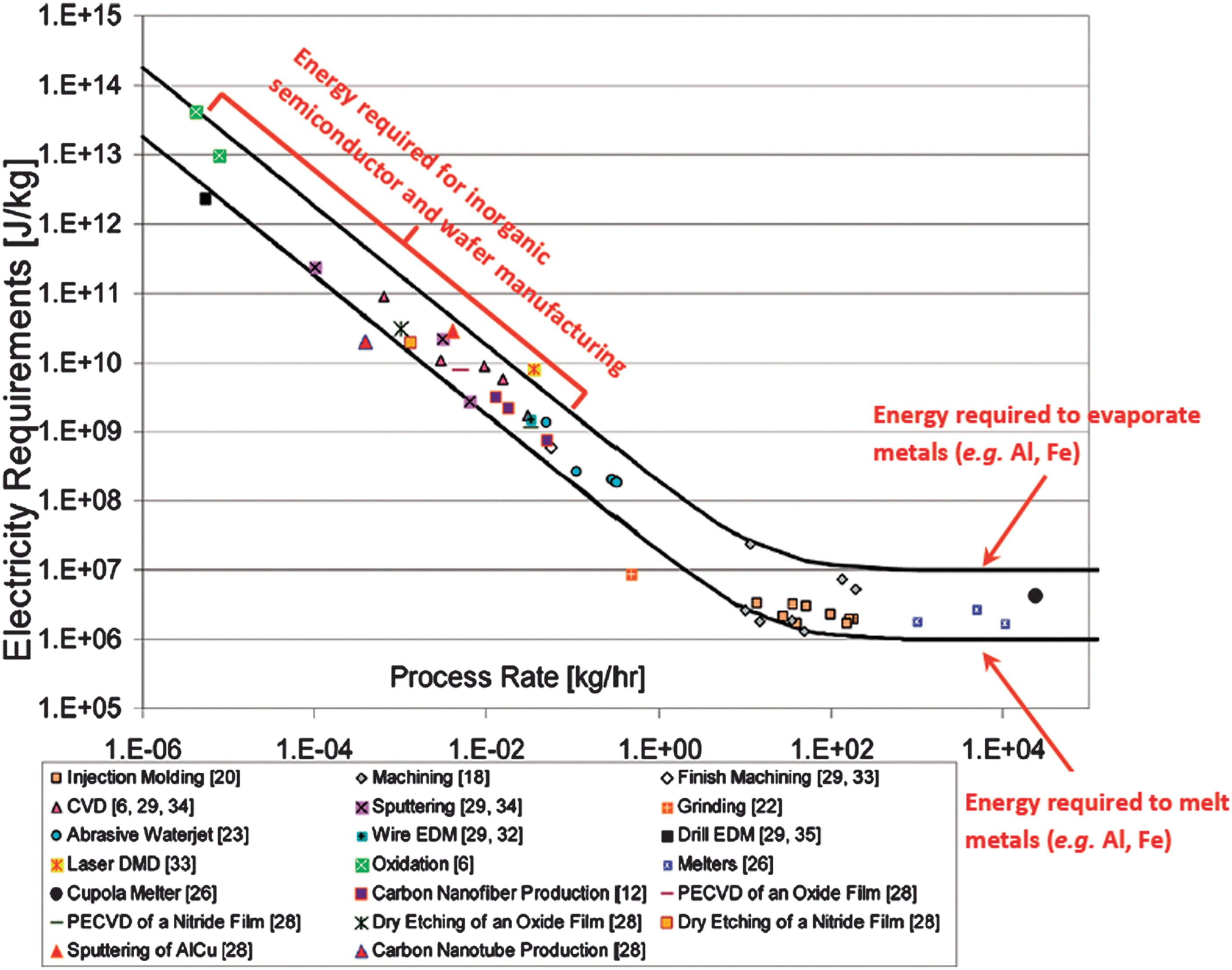 | ||
| Fig. 1 Work in the form of electricity used per unit of material processed expended in twenty typical manufacturing techniques, as a function of the rate of material processed (numbers in brackets represent the references cited therein). Adapted and reprinted with permission from T. G. Gutowski, M. S. Branham, J. B. Dahmus, A. J. Jones, A. Thiriez, and D. P. Sekulic, Thermodynamic Analysis of Resources Used in Manufacturing Processes, Environ. Sci. Technol., 2009, 43, 1584–1590. Copyright (2009) American Chemical Society. | ||
The colossal demand of electronics is leading not only to the above mentioned energy imbalance, but also to a series of unfortunate and undesirable consequences: (i) a massive amount of waste electrical and electronic equipment (WEEE) and (ii) a rapid exhaustion of already scarce natural elements, such as gallium (annual production of ∼215 tons) and indium (annual production of ∼1100 tons including recycling) both of which have an estimated availability of about 20 years until they will run out completely. USA, EU, China, and Japan are main contributors to the estimated WEEE of the world in excess of 50 million tons per year. Despite imposing tighter regulations, China, India, Pakistan, Nigeria and Ghana import the highest amount (estimated 30%) of the e-waste of the world. In the EU-25 (European Union without counting the newcomers Romania, Bulgaria and Croatia) the amount of WEEE reached 9 million tons per year in 2010, despite the recovery and recycling of ∼66% of own e-waste. A global account of the WEEE is given in Table 1.4 A paradigm shift of the way we control both the resource exploitation and the electronics disposal is required in order to minimize the negative impact of our present and future generations on the environment and to create a sustainable future. As defined by the United Nations World Commission on Environment and Development, a sustainable development is established when humanity ensures its present needs without compromising the ability of future generations to meet their own needs.5
| Country/region | Annual household production in mln tons | Landfilling, storage and incineration in mln tons | Domestic recovery in mln tons | Annual export in mln tons | Annual import in mln tons |
|---|---|---|---|---|---|
| USA | 8.4 | 5.7 | 0.42 | 2.3 | — |
| EU-25 | 8.9 | 1.4 | 5.9 | 1.6 | — |
| Japan | 4.0 | 0.6 | 2.8 | 0.59 | — |
| China | 5.7 | 4.1 | 4.2 | — | 2.6 |
| India | 0.66 | 0.95 | 0.68 | — | 0.97 |
| West Africa | 0.07 | 0.47 | 0.21 | — | 0.61 |
Organic (carbon based) technologies are meant to address the energy and cost inefficiency issues posed by their inorganic counterparts. Organic electronics (based on conjugated polymers or small molecules as the core semiconductor element) entered the research field in the mid-1970s-early 1980s holding the high promise of delivering low-cost and energy-efficient materials and devices. Despite intense effort of the scientific community during the past 30 years, the performance6–8 and stability9 of organic semiconductors remain at current times major hurdles in their development as solid competitors of the inorganic counterparts. As a consequence, the large-scale immediate replacement of hard core inorganic components, like the ones active in high-speed processors, integrated circuits, and even solar cell modules, with organic counterparts is not immediately foreseen.6,7,9,10 Nevertheless, the “soft” nature of carbon-based materials confers them a considerable advantage over the inorganic counterparts, enabling fabrication of extremely flexible, highly conformable and even imperceptibly thin electronic devices.11
“Green” materials are an emerging concept within the carbon-based class, aimed at achieving far more ambitious goals, e.g. integration of electronics into living tissue with the aim of achieving biochemical monitoring, diagnostic, or even drug delivery tasks;12 or generating human and environmentally benign technologies.13 “Green” materials and “green” technologies are carving avenues towards achieving the ambitious goal of sustainability in the field of electronics,14 by identifying (i) highly abundant and low cost organic precursors, with (ii) economically feasible-high throughput synthetic routes that avoid the usage of toxic solvents for the fabrication of electronic grade materials and do not generate toxic waste requiring expensive handling and disposal. In addition, the synthesized electronic grade materials should ensure (iii) low cost processing routes in practical devices (ideally either at room temperature from benign solvents or at low sublimation temperatures), and (iv) render electronics that feature biodegradability in mild degradation conditions at the end of their life cycle and/or electronics that are suitable for performing complex biological functions (e.g. transduction, sensing, recognition, event triggering, etc.) as a tool for interfacing electronics with various forms of life. Since “green” materials and technologies are now in the stage of emerging concepts, offering at this time a clear definition of “greenness” is not unequivocal; that is because achieving industrial synthesis of “green” organic materials by means of “green” technologies (i.e. fulfilling all the criteria i–iv above) remains truly challenging at this time. For example many benign dyes and pigments commonly employed in textile, cosmetic, and food coloring industries are produced through industrially attractive, low cost-high throughput synthesis; nevertheless in many cases their production involves and generates environmentally unfriendly by-products and waste.
In their quest to achieve electronics sustainability by solving the above-mentioned energy deficiency puzzle and redressing the unfolding environmental disaster, scientists are often inspired both by the apparent simplicity and by the true complexity of nature. The vision is to mimic nature for creating a novel class of engineered materials able to deliver complex functions, e.g. reproducing the photosynthesis process by means of a synthetic-leaf;15 fabricating artificial compound eyes with the aid of 3D biomimetic polymers;16 reproducing the intricate nature of natural photonic fibers;17 generating artificially engineered, self-assembled peptide sequences18 that found applications in electronics;19 designing super-hydrophobic (lotus effect),20 super-adhesive (gecko effect)21 or self-healing22 surfaces; reproducing the natural infrared camouflage coatings of cephalopod proteins;23 or even exploiting the spermatozoid motion in a hybrid micro-bio-robot.24 Nature is an extremely efficient energy consumption engine that we could use for infinite inspirations. The diversity of natural materials offers a plethora of unexplored phenomena to researchers, and has already started to open new fields in chemistry, physics, and materials engineering.25–27 An exciting area of cross-disciplinary research field currently emerging is “organic bioelectronics”, where biocompatible materials are implemented in various electronic devices interfaced with living tissue.28 Here the scientists from chemistry, physics, materials science, electrical and mechanical engineering branches contribute to the success of this emerging area of research by designing novel biocompatible (active or passive) materials, conceiving device and circuit layouts, selecting the preferred packaging strategy, to accomplish the outcome of integration and interaction of bioelectronics with living organisms.29,30 “Organic bioelectronics” is therefore envisioned to act as a complementary technology for the immediate future, generating electronic interfaces in emerging fields and new markets, thus decreasing the need for conventional electronics requirement in those emerging areas. Among the successful demonstrations of organic bioelectronics one can enumerate ultra-thin electronic platforms for surgical, point-of-care,31 and diagnostic implants,32 ambient intelligence for daily-life assistance,13 soft robotics,33 conformable and self-sustaining bioelectronic components for sports and recreation,13 or even disposable (biodegradable) electronics34,35 for food packaging36 or throw-away applications.37 The combination of novel electronic constituents with biosensing elements will open the possibility for developing disposable diagnostic and drug-delivery technologies, a topic that has been recently reviewed (ref. 12 and 38–42 and the citations therein). The organic bioelectronics field may prove to be the suitable host for welcoming natural and nature-inspired organic materials and a perfect trampoline for achieving the ambitious goal of “green” and sustainable electronics future.
Many aspects of the highly unusual materials science associated with “green” electronics will be presented in this Review Article. The last ten years have witnessed a series of milestone contributions, which inspired researchers to build up entirely new research directions by applying natural or nature inspired biodegradable or biocompatible organic materials in situations where highly rigid inorganic materials fail. The intention of this Review Article is not only to highlight novel materials and device architectures clustered under the umbrella of “green electronics” but also to expose pathways to be followed by materials designers and synthetic chemists that can ultimately lead to the development of high performance devices and set up for a sustainable organic electronics future. This article is meant to highlight examples rather than provide a comprehensive report of this emerging area of research. The author apologizes for any inadvertent omission of any research group and their activity in this exciting field.
1.2 Emerging natural and nature-inspired materials
Many new ideas and concepts for the application of organic materials have emerged with the goal of matching or even surpassing the performance of inorganic-based electronics: examples include (i) pushing the upper limit of organic photovoltaic (OPVs) efficiency to 20% or more; (ii) fabrication of novel organic light emitting diodes (OLEDs) from band-gap engineered materials; (iii) fabrication of high performance organic field-effect transistors (OFETs) and integrated circuits from high performance active layer materials and (iv) integrating active electronic components with living tissue. The exploration of such concepts and ideas was often hampered by the lack of active materials and processing expertise necessary to fabricate such electronic devices. With OLEDs already making a large footprint in the market of flat panel displays, and with OFETs and OPVs entering small scale commercial production in e-books and roll-to-roll fabricated photovoltaics, respectively, the research field of organic electronics is mature enough to focus on achieving ambitious goals of generating “green” avenues for a sustainable future. The following subchapters are a succinct presentation of recent reports in the field of organic electronics where high performance has been demonstrated with active organic components made of natural or nature-inspired materials. This shows that such “green” materials are not at all inferior to the typical organic counterparts investigated and employed within the past two decades and that they have a yet unrevealed potential for further optimization. The chapter dedicated to these emerging materials is divided into subchapters according to the typical architecture employed in electronics fabrication, starting from outside (i) substrate and encapsulate layers and proceeding to inside (ii) contact electrodes and (iii) dielectric and semiconductors – the actual heart of organic electronics.Semi-natural/semi-synthetic substrates: paper. Historically paper manufacturing dates back to the second century AD in China, but it originates from papyrus production in Egypt, more than 4000 years ago, both paper and papyrus being considered among the greatest discovery of human civilization. Nowadays paper is a ubiquitous material that is roll-to-roll industrially produced worldwide at speeds sometimes exceeding 100 km h−1; its cost per square meter (∼10 cent) is unrivaled by any other substrate for electronics, and is this combination of availability and cost-effectiveness that turned paper into an attractive candidate for electronics development. To be exact, the commercially available paper is neither fully natural nor synthetic material, a denotation of “semi-natural” being somewhat closer to reality. This is because natural cellulose-fiber based substrates are coated with natural mineral pigments (e.g. kaolin) in combination with a synthetic latex binder. The mineral pigments and synthetic latex make the paper substrate not fully biodegradable, but this aspect is often overlooked in the literature, and paper is mostly referred as the “natural substrate”. The past 10 years witnessed many important reports comprising various applications of paper (e.g. energy storage, microfluidics, or thermochromic display). Daniel Tobjörk and Ronald Österbacka recently offered a full account of these highlights in their extensive review.37 In the following, only few of these highly interesting reports will be presented.
Due to its inexpensive structure, lightweight, flexibility and environmental friendliness, paper became an attractive solution for the fabrication of rechargeable batteries for energy storage applications, where high energy density must be coupled with low weight. The factor that triggered this research was the discovery that electronically conductive polymers such as polypyrrole, polyaniline, and polythiophene display high theoretical capacities, ranging from ∼100 to 140 mA h g−1. Importantly, these polymers can be easily oxidized and reduced at very high rates, which is a prerequisite for their usage in high power applications like for example contemporary batteries and supercapacitors – a topic that has been recently reviewed by the research group of Maria Strømme.44 The main challenges for the use of electrically conductive polymer based batteries and supercapacitors are (i) their cycling instabilities, (ii) relatively high self-discharge rates, and low capacities due to their low attainable doping degrees, corroborated with (iii) charge transport limitations through thick conducting polymer layers. Attractively, all the above difficulties could be successfully mitigated by mixing or strengthening these conductive polymers with cellulose fibers, producing a conductive paper material that could be either directly employed as a working electrode or used as the underlying substrate for the electrochemical deposition of conductive metal electrodes, i.e. copper or silver. The resulting devices were also amenable for molding into paper sheets of desired shape to suit any particular application.
In a very elegant demonstration, conductive paper was used by the group of Yi Cui to replace the heavy metallic current collectors, leading to a 20% decrease in the weight of the batteries without a loss in capacity.45 The group used commercial paper as the matrix for integration with 1D nanomaterials (silver nanowires or, alternatively, carbon nanotubes). By employing simple solution processing of active nanomaterials, and taking advantage of the high solvent absorption of the paper and its strong binding to the conductive particles, the resistance of the paper could reach 1 ohm per square (Ω sq−1), recommending paper as a candidate for energy storage applications. The performance reported was impressive: the conductive paper showed remarkable stability over more than 40![[thin space (1/6-em)]](https://www.rsc.org/images/entities/char_2009.gif) 000 charge–discharge cycles with only 3% and 0.6% capacitance loss in a sulfuric acid electrolyte and an organic electrolyte respectively. Importantly, the mechanical stability of the paper remained intact during the 60 days operation test. The results of the group are summarized in Fig. 2-top, showing (A) the geometry of the paper-based energy storage device with paper acting as a current collector for the Li-ion battery; (B) galvanostatic charge–discharge curves of LiMn2O4 nanorod cathode and Li4Ti5O12 nanopowder anode half-cells and (C) excellent cycling performance of LiMn2O4 nanorod (C/3 = 49 mA g−1) and Li4Ti5O12 nanopowder (C/3 = 58 mA g−1) half-cells. This work demonstrates that paper-based energy storage technology has the potential to be combined with other types of electronic devices to achieve integrated electronic circuits on a single chip of paper. Although such an integrated system has not yet been reported, the following subsections dedicated to paper based electronics provide some food for thought.
000 charge–discharge cycles with only 3% and 0.6% capacitance loss in a sulfuric acid electrolyte and an organic electrolyte respectively. Importantly, the mechanical stability of the paper remained intact during the 60 days operation test. The results of the group are summarized in Fig. 2-top, showing (A) the geometry of the paper-based energy storage device with paper acting as a current collector for the Li-ion battery; (B) galvanostatic charge–discharge curves of LiMn2O4 nanorod cathode and Li4Ti5O12 nanopowder anode half-cells and (C) excellent cycling performance of LiMn2O4 nanorod (C/3 = 49 mA g−1) and Li4Ti5O12 nanopowder (C/3 = 58 mA g−1) half-cells. This work demonstrates that paper-based energy storage technology has the potential to be combined with other types of electronic devices to achieve integrated electronic circuits on a single chip of paper. Although such an integrated system has not yet been reported, the following subsections dedicated to paper based electronics provide some food for thought.
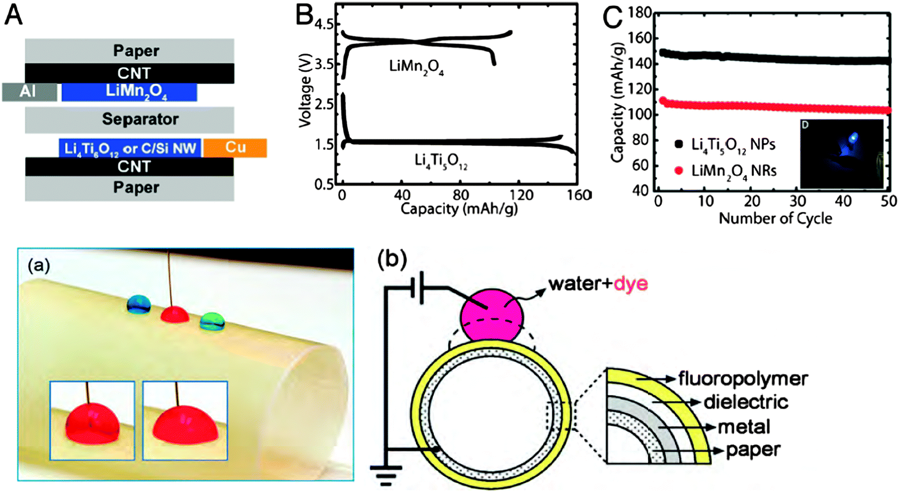 | ||
| Fig. 2 (top A) Schematic of conductive paper as a current collector for the Li-ion battery; (top B) galvanostatic charge–discharge curves for the LiMn2O4 nanorod cathode and the Li4Ti5O12 nanopowder anode; (top C) cyclic performance of the anode and cathode half cells, with the inset showing the paper based battery source as the energy supply to light a blue LED. Reproduced with permission from L. Hu, J. W. Choi, Y. Yang, S. Jeong, F. La Mantia, L. F. Cui, and Y. Cui, Highly Conductive Paper for Energy-storage Devices, Proc. Natl. Acad. Sci. U. S. A., 2009, 106, 21490–21494; (bottom a) representation of the electrowetting display mechanism on a paper substrate, showing the variation in the wetting angle of the aqueous droplet with applied voltage; (bottom b) schematic of the fabricated device. Reproduced with permission from D. Y. Kim and A. J. Steckl, Electrowetting on Paper for Electronic Paper Display, ACS Appl. Mater. Interfaces, 2010, 2, 3318–3323. Copyright (2010) American Chemical Society. | ||
One such integration possibility would be to take advantage of the usage of paper as the substrate for the formation of electronic displays based on the electrowetting (EW) effect (i.e. the action of electric fields on the wetting of solid surfaces). In a very nice demonstration, the research group of Andrew Steckl revealed the possibility to fabricate “e-paper” displays directly on paper, therefore providing a colorful alternative to the classic monochromatic electrophoretic-based technology for e-reader devices.46 The group investigated various types of commercially available paper substrates, with surface roughness, coating properties, water uptake and thickness as critical parameters to be considered in order to replicate the look-and-feel of actual ink-on-paper. Fig. 2-bottom depicts three deionized (DI) water droplets containing soluble dyes placed on a rolled-paper EW device (panel a) and the schematic of their approach, consisting of a glassine paper substrate, a ground electrode, a dielectric layer, and a fluoropolymer top layer (panel b). When a conducting wire is placed into the red droplet, and an external voltage is applied, the electrowetting effect is demonstrated, via a noticeable change in the contact angle (the two insets of panel a). The electrowetting devices reported in this work showed large contact angle modulation (∼90°) and relatively fast switching speed in the range of few tens of milliseconds, which are basic prerequisites for many electrowetting applications, including video display. Importantly, the latter report proves that widely available, cheap and environmentally friendly paper substrates can be integrated into high performance electronics that have biodegradability as the main feature of their end-life.
Paper traditionally consists of layers of random networks of cellulose fibers having variable fiber length, diameter, and density. Many of the traditional approaches addressed the high surface roughness and porosity nature of the paper (the factors that made deposition of subsequent layers unrealizable) by covering its surface with smoothening layers (e.g. by deposition of a smooth plastic film) or even gluing the electronics directly on paper. In the examples below, a few models are presented that could overcome the already mentioned challenges through alternative engineering techniques. In a very elegant demonstration, the group of Hagen Klauk showed that electronics could be directly fabricated on the rough surface of typical banknotes, which could potentially suit various anti-counterfeiting applications (Fig. 3-top left).47 Their approach consisted of all-dry deposition conditions, except for a short solvent exposure during the growth of the self-assembled monolayer dielectric. Interestingly, the array of devices fabricated on rough banknote substrates showed highly similar and reproducible transistor characteristics, with only two devices out of 100 falling out of the desired operational range (Fig. 3-top center and right panels). Further, simple integrated circuits have been demonstrated, reaching quasi-static inverter gains of ∼100 and switching speeds of ∼2 kHz, values that are remarkable for devices fabricated on such challenging substrates. Importantly, these results lie within one order of magnitude below the best reported switching speeds of electronics fabricated on smooth plastic substrates (ref. 47 and references cited therein) and within two orders of magnitude below the performance of aggressively optimized and scaled down ring oscillators based on the same semiconductor material (i.e. DNTT), fabricated on smooth glass substrates.10
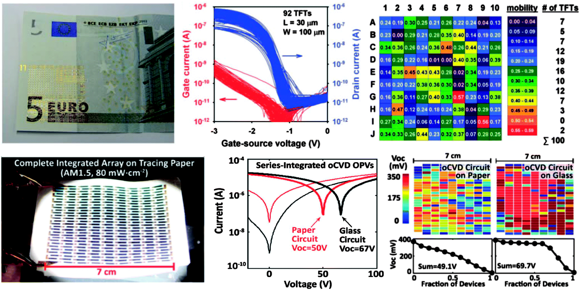 | ||
| Fig. 3 (top-left) Photograph of an array of transistors for anti-counterfeiting applications fabricated directly on the rough surface of a 5-Euro banknote; (top-center) transfer characteristics of 92 functional transistors out of 100 fabricated transistors with DNTT as the organic semiconductor; (top-right) statistical distribution of the maximum drain current. The field-effect mobility, the on/off ratio, and the maximum gate current are presented in the right columns. Reproduced with permission from U. Zschieschang, T. Yamamoto, K. Takimiya, H. Kuwabara, M. Ikeda, T. Sekitani, T. Someya, and H. Klauk, Organic Electronics on Banknotes, Adv. Mater., 2011, 23, 654–658. Copyright Wiley-VCH Verlag GmbH & Co. KGaA. (bottom-left) Photograph of a large-area monolithic array of photovoltaic cells fabricated on commercial (unmodified) paper; (bottom-center) current–voltage (C/V) curves for the integrated photovoltaic arrays with vapor-patterned electrodes on paper (red type) and glass (black type) under illumination and in the dark (bold and thin lines respectively); (bottom-right) spatial map of the open circuit voltage of individual cells in the array. Reproduced with permission from M. C. Barr, J. A. Rowehl, R. R. Lunt, J. Xu, A. Wang, C. M. Boyce, S. G. Im, V. Bulovic, and K. K. Gleason, Direct Monolithic Integration of Organic Photovoltaic Circuits on Unmodified Paper, Adv. Mater., 2011, 23, 3500–3505. Copyright Wiley-VCH Verlag GmbH & Co. KGaA. | ||
Managing to solve the critical issue of adherence of the first monolayers of organic material to the rough and porous surface of the “as purchased” (unmodified) paper (see Fig. 3-bottom left), the research group of Vladimir Bulovic demonstrated high performance solar cell structures integrated on a paper-based module.48 By applying oxidative chemical vapour deposition of organic electrodes (PEDOT), the subsequent deposition and the functionality of the organic layers were not hampered by the roughness and porosity of the underlying substrate. A thin passivation layer, allowing the module to work for over 6000 hours and retain its operability even when submersed in water, capped the 250 solar cell integrated structure. Interestingly, the performance of the module fabricated on the paper substrate compared favourably to the one of a similar structure deposited on glass (Fig. 3-bottom center and right panels).
The proof-of-principle examples presented in Fig. 3 demonstrate that when all the critical steps are taken into consideration and the design is carefully engineered, conventional paper in its ubiquitous, low-cost version can employed for the fabrication of flexible, deformable, high performance integrated circuits. Interestingly, the novelty of the latter two approaches eliminates the need for more costly and heavier substrates such as ultra-smooth plastics, while leaving room for further improvement and optimization.
Biocompatible substrates: synthetic polymers. “Green” materials and technologies have been recently developed to address the biodegradability and biocompatibility issues faced by most of the inorganic electronics, and to allow benign integration of electronics with living tissue, with a vision of slowing down the requirement of classic (inorganic) materials for such applications. Due to their inertness, low density polyethylene (LDPE) and polydimethylsiloxane (PDMS) have been accepted by the US National Heart, Lung and Blood Institute as discriminatory tools for validation of both in vivo and in vitro tests in the evaluation of biomaterials.49 Owing to its excellent biocompatibility, hemocompatibility and inflammatory resistance, PDMS recently became the synthetic substrate of choice for the fabrication of biocompatible electronic platforms. In a recent demonstration, Stephanie Lacour's group developed implantable compliant electrodes fabricated from a gold microelectrode array embedded within four parallel polydimethylsiloxane (PDMS) microchannels for monitoring the bladder nerve function.50 The resistance to deterioration of the electrode array immersed in phosphate buffered saline exceeded three months suggesting that the electronic system could be implanted into living tissue. Employing a tripole electrode configuration to maintain the background noise low and improve the signal-to-noise ratio, the group reported the disambiguous recording of two types of bladder nerve activity (filling and contraction). This demonstration is the first report of multichannel recordings of bladder afferent activity by means of stretchable electrodes built on a biocompatible elastomer platform. This type of implantable neural prosthesis could help restore the bladder function by monitoring the bladder fullness and stimulate its emptying. Apart from PDMS, other synthetic materials are currently employed in the fabrication of implantable devices. Such synthetic polymers comprise parylene, polylactic acid (PLA), polylactic-co-glycolic acid (PLGA), polyethylene glycol (PEG), poly(2-hydroxyethyl methacrylate) (pHEMA), polyurethane (PU), and polyvinyl alcohol (PVA). A full account of such materials for regenerative medicine has been recently reported in excellent reviews, and further examples of such functional molecules are depicted in Fig. 4.51,52
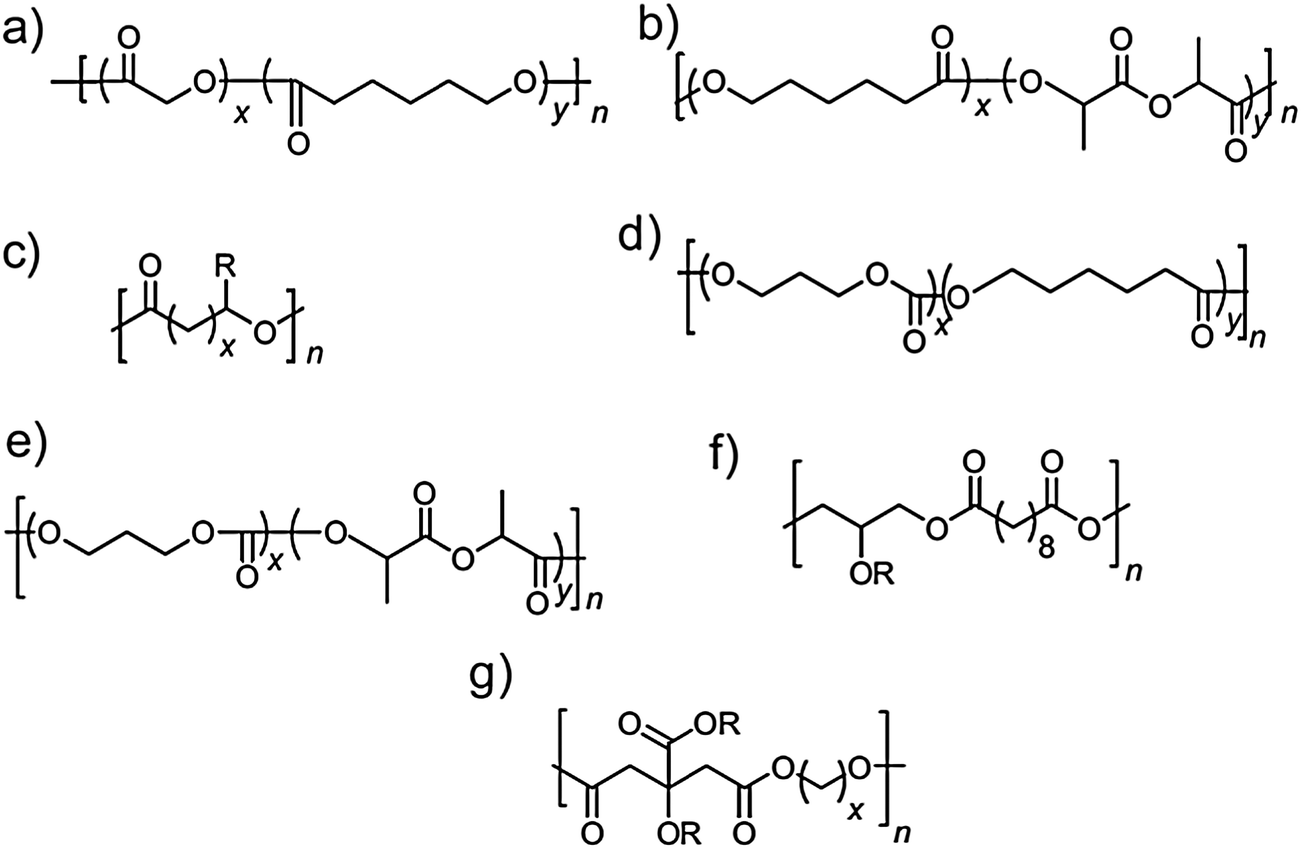 | ||
Fig. 4 General chemical formula of few examples of biodegradable polyester elastomers. A complete list of such polymers is presented in ref. 52. (a) Poly(glycolide-co-ε-caprolactone), (b) poly(lactide-co-ε-caprolactone), (c) polyhydroxyalkanoates, (d) poly(trimethylene carbonate-co-ε-caprolactone), (e) poly(trimethylene carbonate-co-D,L-lactide), (f) poly(glycerol sebacate), and (g) poly(diol-co-citrate); R![[double bond, length as m-dash]](https://www.rsc.org/images/entities/char_e001.gif) H, side chain. Reproduced with permission from M. C. Serrano, E. J. Chung, and G. A. Ameer, Advances and Applications of Biodegradable Elastomers in Regenerative Medicine, Adv. Funct. Mater., 2010, 20, 192–208. Copyright Wiley-VCH Verlag GmbH & Co. KGaA. H, side chain. Reproduced with permission from M. C. Serrano, E. J. Chung, and G. A. Ameer, Advances and Applications of Biodegradable Elastomers in Regenerative Medicine, Adv. Funct. Mater., 2010, 20, 192–208. Copyright Wiley-VCH Verlag GmbH & Co. KGaA. | ||
Polyvinyl alcohol (PVA) is another example of synthetic polymer that has biocompatible properties and has been recently employed as a substrate for the fabrication of biodegradable and biocompatible electronics.29,34 PVA is a water soluble polymer that forms flexible layers and advantageously, when used as a substrate and/or a coating layer for implantable device applications, allows the controlled transport of water soluble analytes by means of altering the crosslinking density of the chains and their subsequent swelling ratio. A demonstration of high performance electronics fabricated on a sacrificial PVA substrate was performed by John Rogers's group, which reported integrated devices for physiological measurement and stimulation that exploit interfaces to the human epidermis. One example is depicted in Fig. 5, where the integrated circuit containing a collection of multifunctional sensors (i.e. temperature, strain and electrophysiological), active–passive circuit elements (i.e. diodes, resistors and transistors), miniaturized light emitting diodes, wireless power transmitter coils and high-frequency inductors, capacitors, oscillators and antennae have all been integrated on the surface of a thin PDMS foil on top of a water soluble PVA sheet.29
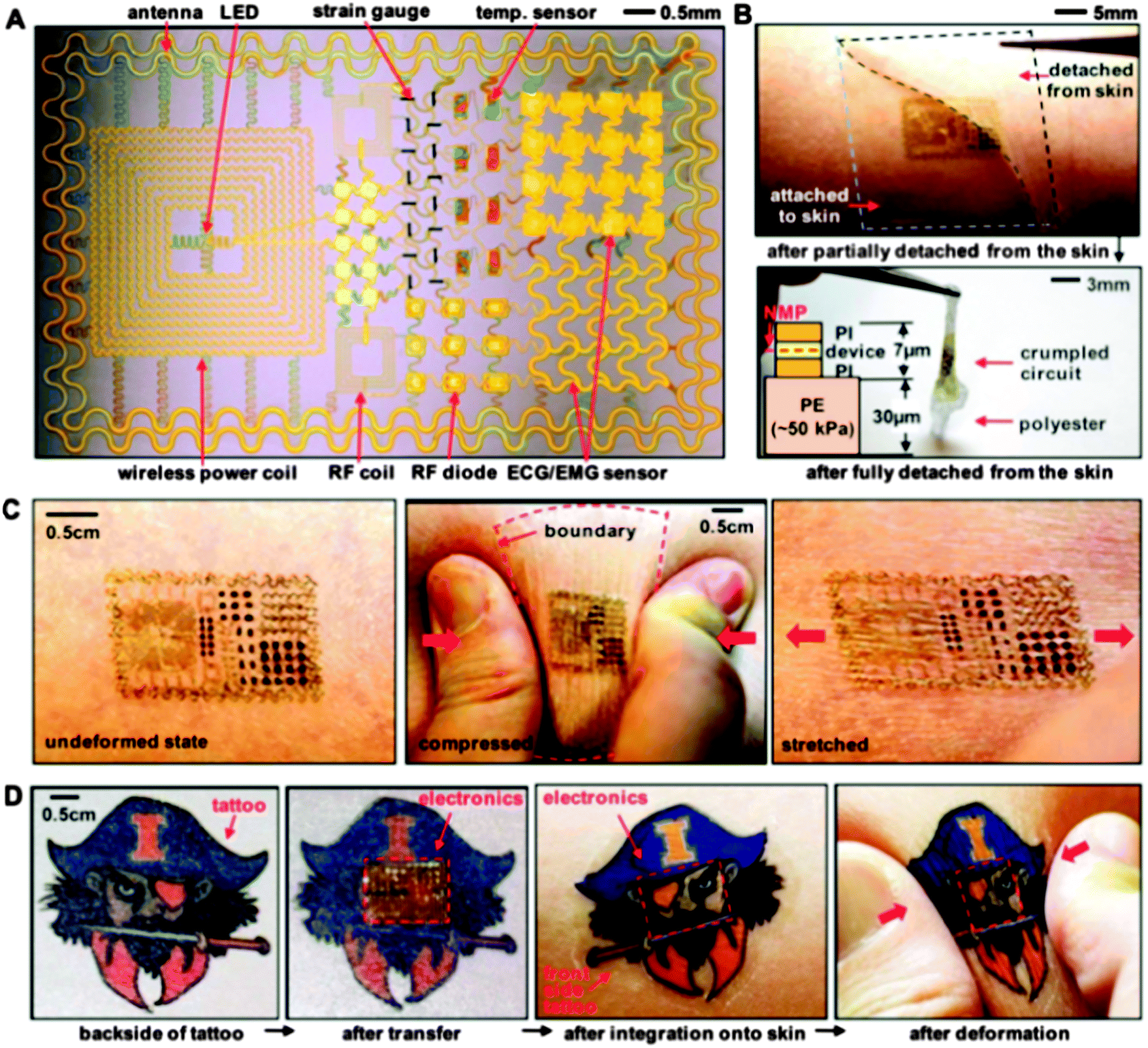 | ||
| Fig. 5 Demonstration of complex circuits for bio-integrated electronics. (A) Photograph of an electronic circuit that contains an antenna, a LED, a strain gauge, a temperature sensor, wireless power coils, radio frequency coils, and various sensors monitoring the brain and the heart functions of the patient. (B) Fabrication procedure showing the circuit on top of a sacrificial, water-soluble film of PVA that is subsequently transferred face-down onto the human epidermis and remains conformably attached to the skin through van der Waals forces. (C) and (D) Example of potential applications of bio-integrated electronics, as multifunctional tattoos showing resistance to various states of stress. From D.-H. Kim, N. Lu, R. Ma, Y.-S. Kim, R.-H. Kim, S. Wang, J. Wu, S. M. Won, H. Tao, A. Islam, K. J. Yu, T. Kim, R. Chowdhury, M. Ying, L. Xu, M. Li, H.-J. Chung, H. Keum, M. McCormick, P. Liu, Y.-W. Zhang, F. G. Omenetto, Y. Huang, T. Coleman, and J. A. Rogers, Epidermal electronics, Science 2011, 333, 838–843. Reprinted with permission from American Association for the Advancement of Science (AAAS). | ||
The sacrificial layer of the soluble polymer served as a temporary support for the transport and mounting of the device onto the skin, in a similar fashion to the function of a temporary transfer tattoo. This work represents a remarkable demonstration that organic materials enable high performance flexible functionalities that can be intimately and invisibly integrated with living tissue. Beyond the demonstration level, many hurdles lie ahead in the development of tissue-integrated electronics, like for example fabricating electronics from materials that can accommodate the continuous effluence of dead cells from the surface of the skin or withstand the process of transpiration. Perhaps the highest obstacle to be overcome in the development of bio-integrated electronic functionalities is the circumvention of the foreign-body reaction of the host tissue to the implant. The latter reaction of the living tissue results in the formation of a dense collagenous capsule surrounding the implant, which blocks the ionic and electronic transport between the implant and the body and renders the device ineffective.51 Recent work of Shaoyi Jiang's group went in the direction of solving this major inconvenience.53 The group reported zwitterionic hydrogels based on poly(carboxybetaine methacrylate) (PCBMA) prepared from a carboxybetaine monomer (CBMA) and a carboxybetaine cross-linker (CBMAX). Comparing this novel hydrogel with the typical candidate for such development (pHEMA) – see Fig. 6 – the group observed a reduced inhibition of angiogenesis near PCBMA hydrogels three months after implantation, which demonstrated that PCBMA has superior potential to pHEMA in facilitating mass transport between the body and the implanted device. The latter report paves the way for further development and optimization of a novel class of implantable/ingestible electronic devices where the intimate contact with living tissue dictates their functionality.54
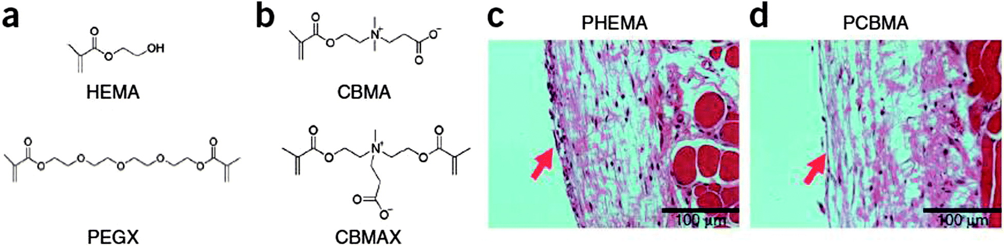 | ||
| Fig. 6 (a and b) Chemical formula of the monomer hydrogels (HEMA and CBMA) and their respective cross-linkers (PEGX and CBMAX). (c and d) Such biocompatible hydrogels were employed in the evaluation of foreign body response towards the implanted devices in mice, with the implant to tissue interface highlighted by red arrows. Reprinted with permission from Macmillan Publishers Ltd: L. Zhang, Z. Cao, T. Bai, L. Carr, J.-R. Ella-Menye, C. Irvin, B. D. Ratner, and S. Jiang, Zwitterionic Hydrogels Implanted in Mice Resist the Foreign-body Reaction, Nat. Biotechnol., 2013, 31, 553–556. Copyright (2013). | ||
Fully biocompatible and biodegradable substrates: natural silk, shellac, hard gelatin. Naturally occurring materials employed as biocompatible and biodegradable substrates for various electronics applications include collagen, chitin, chitosan, alginate, dextran, shellac, hard gelatin and silk (ref. 27 and 51 and references cited therein). The following subchapter presents a highlight of remarkable reports on such natural substrates for organic electronics applications.
Silk is a biocompatible, natural protein fiber that emerged as a prime candidate for the development of electronics interfaced with living organisms. Silk is composed of fiber strands of varying length connected laterally by at least two or three backbone hydrogen bonds, thus leading to a generally twisted pleated sheet, which together with other such layers assembles into a series of antiparallel sheets. Constituently, the chemical structure of silk can be expressed as the recurrent amino acid sequence glycine, serine and alanine, i.e. (Gly-Ser-Gly-Ala-Gly-Ala)n. The glycine content allows for tight packing of the beta sheets, and contributes to its rigid structure and high tensile strength. Given its amazing mechanical properties, flexibility, chemical stability, and ease of processing, silk records steady demand in textile and medical suture applications. The Fig. 7-green frame shows the recent breakthrough in silk technology that allowed the ancient material to successfully tap into various high-tech biomedical fields, including electronics and photonics.25 Due to its biocompatibility and controlled biodegradability, silk was employed as a platform for the fabrication of electronics for food sensing applications,36 improved physiological recording and targeted drug delivery,55 as well as biomedical implants.56 The silk films and fibers show controllable degradation rate, tunable from minutes to days, and it is this combination of versatility, biocompatibility, low cost and ease of processing that recommends this naturally occurring protein for a broad scale of applications in various environmentally compatible systems as well as implantable optical systems for diagnosis and treatment. An example of implantable electronics fabricated on a silk substrate will be presented in the following section, dealing with biocompatible electrodes.
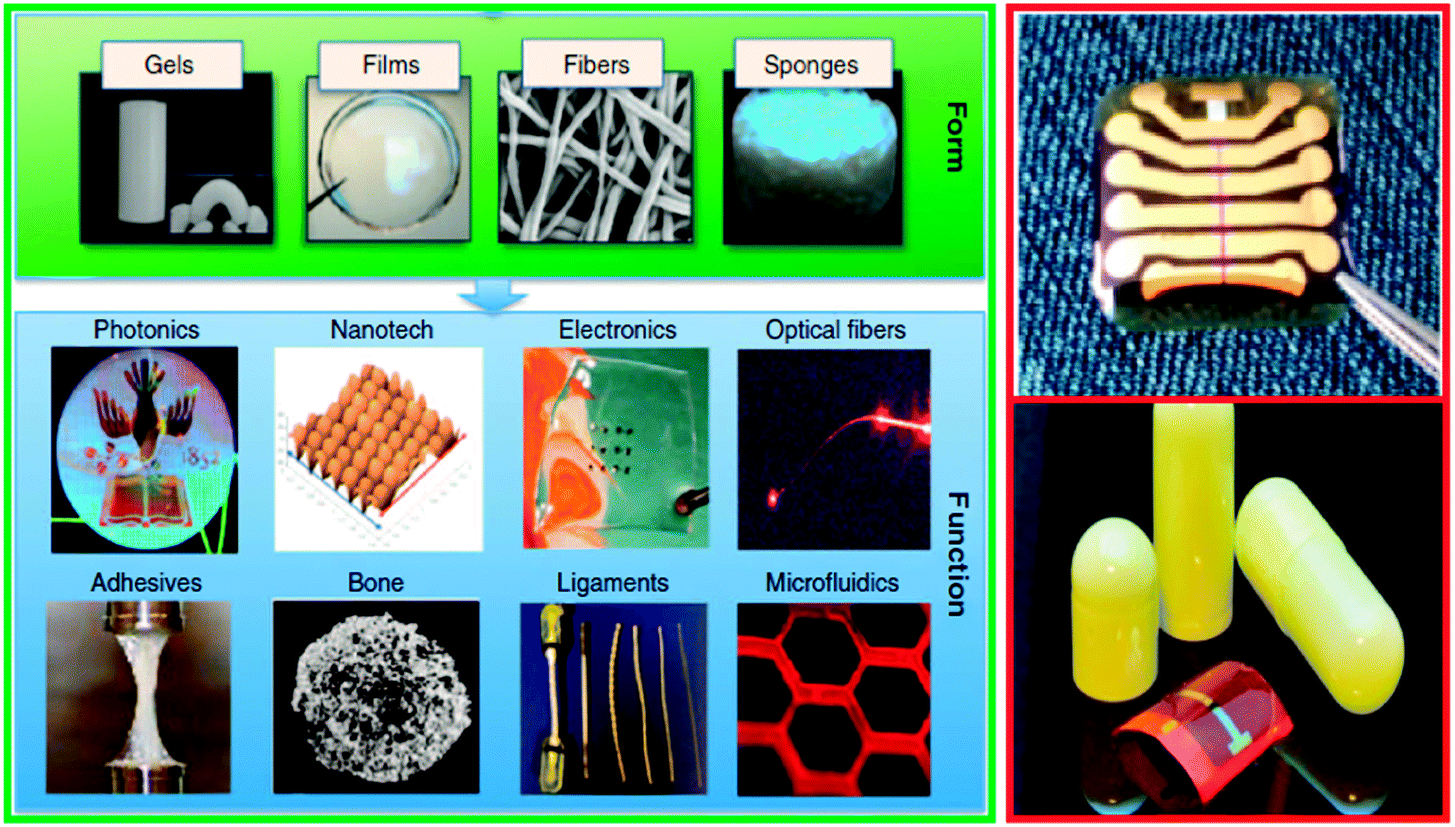 | ||
| Fig. 7 (green frame) Examples of materials that can be fabricated from silk in various shapes and forms, leading to functional devices and technology platforms for various research fields. From F. G. Omenetto and D. Kaplan, New Opportunities for an Ancient Material, Science, 2010, 329, 528–531. Reprinted with permission from American Association for the Advancement of Science (AAAS); (red frame-top) a series of field effect transistors featuring all natural and biodegradable materials: shellac substrate, aluminum oxide and tetratetracontane dielectric and indigo semiconductor. Electrodes were made of aluminum and gold. Reproduced with permission from M. Irimia-Vladu, E. D. G1owacki, P. A. Troshin, G. Schwabegger, L. Leonat, D. K. Susarova, O. Krystal, M. Ullah, Y. Kanbur, M. A. Bodea, V. F. Razumov, H. Sitter, S. Bauer and N. S. Saricifci, Indigo - A Natural Pigment for High Performance Ambipolar Organic Field Effect Transistors and Circuits, Adv. Mater., 2012, 24, 375–380. Copyright Wiley-VCH Verlag GmbH & Co. KGaA; (red frame-bottom) conformable field effect transistors fabricated on a biodegradable and biocompatible hard gelatin substrate with adenine and guanine as the organic dielectric and perylene bisimide as the organic semiconductor. Rosolic acid in ethanol was used as the smoothening layer; electrodes were all made of gold. Reproduced with permission from M. Irimia-Vladu, P. A. Troshin, M. Reisinger, L. Shmygleva, Y. Kanbur, G. Schwabegger, M. Bodea, R. Schwödiauer, A. Mumyatov, J. W. Fergus, V. Razumov, H. Sitter, N. S. Sariciftci, and S. Bauer, Biocompatible and Biodegradable Materials for Organic Field-Effect Transistors, Adv. Funct. Mater., 2010, 20, 4069–4076. Copyright Wiley-VCH Verlag GmbH & Co. KGaA. | ||
Shellac and hard gelatin are other examples of low cost natural materials extensively employed worldwide by various industries. Shellac, for example, has been known for more than 4000 years for its smoothening and water repellent properties, and was extensively employed by wood craftsman as finishing for high quality furniture. Recently shellac has been introduced by the food manufacturing industry as the edible coating layer preserving the freshness of various fruits and vegetables during transportation. Shellac is in fact a versatile natural material, a natural bio adhesive polymer that is composed of a complex mixture of aliphatic and alicyclic hydroxy acids, and can be considered a natural form of plastic. Shellac has excellent dielectric properties and when deposited as thin films by spin coating can function as both a dielectric and a smoothener.57,58 Hard gelatin is nowadays the material of choice for the manufacture of drug delivery capsules by the pharmaceutical industry. Owing to their smooth surface and excellent film forming properties, shellac and hard gelatin were recently reported by the research group of the author as suitable substrates for high performance electronics featuring all-natural layers (Fig. 7-red frame).
In a recent demonstration, the research group of John Rogers showed that gold electrode arrays sandwiched between thin polyimide foil (to make handling possible) and subsequently deposited on sacrificial silk substrates could be implanted by placing them on the exposed brain surface. The gold meshed electrodes could be conformably wrapped on the brain tissue by flushing with saline solution to dissolve away the underlying silk substrate56 (Fig. 8-green frame). Not surprisingly, the thinnest of the mesh electrodes employed (i.e. 2.5 μm thick) displayed the best performance in terms of average evoked response from each electrode. The bottom of the green frame in Fig. 8 depicts the representative single-channel data from one of the 2.5 μm mesh electrodes, where a sleep spindle with a good signal amplitude and signal-to-noise ratio is recorded.
 | ||
| Fig. 8 (green frame) Photograph of an electrode array implanted onto the surface of a cat brain and the average evoked response of each individual sensor. The color of the sensor represents the ratio of the rms amplitude of each average electrode response in the 200 ms period immediately after the presentation of the visual stimulus to the rms amplitude of the average in the 1.5 s period prior to the stimulus appearance. The typical voltage response of each individual sensor is graphically displayed at the bottom of the window. Reprinted with permission from Macmillan Publishers Ltd: D.-H. Kim, J. Viventi, J. J. Amsden, J. Xiao, L. Vigeland, Y.-S. Kim, J. A. Blanco, B. Panilaitis, E. S. Frechette, D. Contreras, D. L. Kaplan, F. G. Omenetto, Y. Huang, K.-C. Hwang, M. R. Zakin, B. Litt, and J. A. Rogers, Dissolvable Films of Silk Fibroin for Ultrathin Conformal Bio-integrated Electronics, Nat. Mater., 2010, 9, 511–517. Copyright (2010); (red frame) polymerization of PEDOT filaments directly on the brain of a mouse. (A) Photograph of the utilized setup comprising a micro wire electrode inserted into the gelatin-stabilized tissue of the mouse brain. A platinum wire is used as the reference/counter electrode. (B–D) Polymerized PEDOT cloud in the mouse brain that is directly integrated into the tissue. From S. M. Richardson-Burns, J. L. Hendricks, and D. C. Martin, Electrochemical Polymerization of Conducting Polymers in Living Neural Tissue, J. Neural Eng., 2007, 4, L6–L13, DOI: 10.1088/1741-2560/4/2/L02 © IOP Publishing. Reproduced with permission. All rights reserved. | ||
A major advantage of the polymer electrodes over their metallic counterparts is the possibility to controllably transport neurotransmitters in their ionic form, therefore paving the way for achieving the recognition and modulation of the event signals by relying on chemical interaction as opposed to the influence of electric fields that is the governing mechanism of metal electrodes. In the first report of the kind, the conducting polymer PEDOT:PSS has been polymerized by the research group of David Martin directly into the living neural tissue of the mouse brain.61 The cloud of PEDOT filaments penetrate far beyond the region that normally develops as fibrous scar tissue and reaches the surrounding of healthy neurons (Fig. 8-red frame). The higher resolution images of the sub-panels C and D prove that the interface of the electrode with the tissue is embedded in a cloud of PEDOT that appears to have developed within the extracellular and interstitial spaces. The polymerized PEDOT forms also extracellular matrix components like fibrils, chains and filaments that are knitted around and between cells and maintain high cell viability. This powerful demonstration supports the viability of intimate, 3D interfacing between soft, low impedance, diffuse and electrically functional conducting polymer networks on one side and living cells on the other.
In a nice follow-up demonstration, the research group of George Malliaras offered an alternative technique to electrochemical polymerization of PEDOT:PSS, other than being grown on pre-patterned metal electrodes.62 The group managed to photolithographically define microelectrodes based on poly(3,4-ethylenedioxythiophene) doped with poly(styrene sulfonate) (PEDOT:PSS) on a biocompatible and highly flexible/conformable, sacrificial parylene substrate with the thickness of only 4 μm. After transplantation in vivo, the layer of parylene could be easily dissolved, exposing the patterned conducting polymer electrodes. The fabricated conducting polymer electrodes were successfully tested against a silicon probe and were subsequently implanted on the surface of the brain of a mouse, with the aim of performing in vivo electrocorticography (ECoG) measurements of sharp waves mimicking epileptic spikes. Interestingly, due to their higher degree of conformability to the surface of the brain, the soft conducting polymer electrodes were shown to outperform gold electrode arrays deposited on the same spot. As a consequence and extension of this fabrication scheme, the reported procedure could be applied to a wider range of conducting polymers, not only PEDOT:PSS.
In order to fully realize the implantable devices, the development of layers or materials with an intermediate functionality is extremely important. One such element is the interconnect layer. In a recent important contribution, the research group of Ching Wong fabricated water based isotropically conductive adhesives (ICAs)63 based on the biocompatible polymer polyurethane.51 The waterborne polyurethane ICAs (having the synthetic scheme reproduced in Fig. 9) represent an excellent alternative to the conventional oil based counterparts. The group controlled the electrical conductivity of the adhesives by adding silver nanoparticles that can be sintered at temperatures below 200 °C. The resulting water based ICAs display rheological properties adjustable relative to the water content, making them compatible with many high throughput printing techniques like screen printing, gravure, and roll-to-roll printing for applications including electrical interconnects and low cost printed circuits.
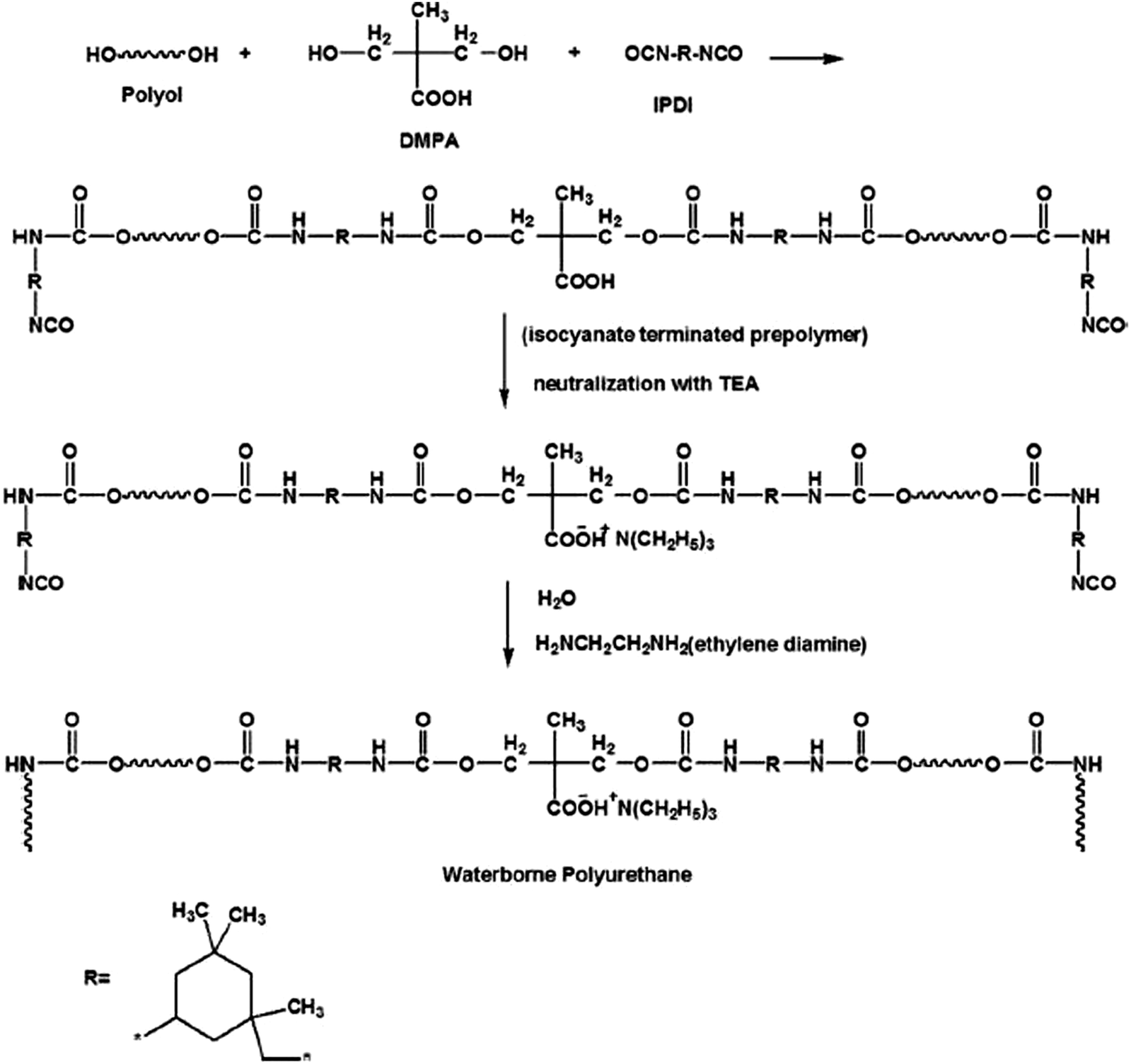 | ||
| Fig. 9 Synthetic route for the fabrication of waterborne polyurethane dispersant for the isotropically conductive adhesive with the curing step at room temperature. Reproduced with permission from C. Yang, W. Lin, Z. Li, R. Zhang, H. Wen, B. Gao, G. Chen, P. Gao, M. M. F. Yuen, and C. P. Wong, Water-Based Isotropically Conductive Adhesives: Towards Green and Low-Cost Flexible Electronics, Adv. Funct. Mater., 2011, 21, 4582–4588. Copyright Wiley-VCH Verlag GmbH & Co. KGaA. | ||
In a very important contribution, the research group of Mehmet Sarikaya demonstrated the possibility to functionalize peptide sequences that have specific binding affinities for various inorganic substrates.64 The group applied the combinatory strategy to develop a genetically engineered quartz-binding peptide sequence at the dielectric–semiconductor interface for the precise control of threshold voltage in organic field effect transistors (Fig. 10). The peptide sequence is a series of various amino acids linked by covalent bonds between the carboxyl group of one molecule and the amino group of the other (i.e. the peptide bonds). Due to the polar nature of the constituents, their structures can produce electric dipoles as a result of their peptide bonds and particular side chains. The precise adjustment of their sequence, structure and/or conformation can affect the generated dipoles and consequently render external control over their binding abilities to various surfaces of interest, including for example dielectric layers for OFET applications. From one perspective, the genetically engineered peptide sequence can be seen as a natural version of the self-assembly monolayer (SAM),6 but the advantages over the traditional synthetic silane or phosphonic acid SAMs are great: the peptide sequence can be processed from benign aqueous solvents, and has the potential to be preferentially engineered and optimized for each surface of interest. Although the research is currently in the stage of identifying peptide sequences to selectively bind the inorganic surfaces, the concept has a tremendous potential to be extended for preferential binding to any organic material. A more powerful concept would be to synthesize peptide sequences attached directly to natural or nature-inspired organic semiconductor small molecules (for example indigo, Tyrian purple, quinacridone, epindolidione – see next subchapter), in order to achieve the hybrid SAM–semiconductor sequence, in other words, the dielectric and semiconductor layers fused in one single molecule for high performance OFET development. This particular concept would take advantage of the inherent ordering of the peptide self-assembly on the inorganic surface of interest and transpose this high degree of ordering to a long range arrangement of the semiconductor tail of the molecule, allowing for charge delocalization and transport through the semiconductor. In addition, the engineered peptide sequences for both inorganic as well as organic binding may turn out to be the perfect candidates for the development of next generation of organic electrochemical transistors (OECTs) for sensing and signal transduction applications (more on the OECT topic will be presented in Section 2.1).
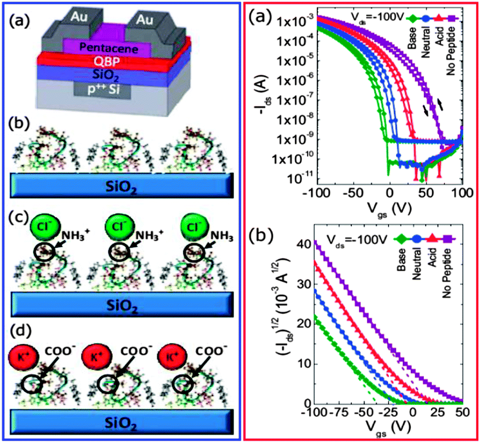 | ||
| Fig. 10 (blue frame-a) Schematic of the thin film transistor device with the peptide-modified dielectric layer for threshold voltage control; (blue frame-b) assembly of the quartz-binding peptide on the dielectric surface in water, (blue frame-c) in hydrochloric acid and (blue frame-d) in potassium hydroxide. Only in the presence of KOH solution, the C-termini of the peptide sequence pair with potassium ions to produce a dipole pointing towards the dielectric surface. (red frame-a) Transfer characteristics of pentacene-based OFETs with the quartz binding peptide sequence assembled in various media; (red frame-b) threshold voltage control achieved by means of the self-assembly peptide sequence. Reprinted with permission from A. Dezieck, O. Acton, K. Leong, E. E Oren, H. Ma, C. Tamerler, M. Sarikaya, and A. K. Y. Jen, Threshold Voltage Control in Organic Thin Film Transistors with Dielectric Layer Modified by a Genetically Engineered Polypeptide, Appl. Phys. Lett., 2010, 97, 013307. Copyright (2010), American Institute of Physics. | ||
Fully resorbable and biodegradable dielectrics for OFET applications were recently reported, stirred by the contribution of Christopher Bettinger and Zhenan Bao.34 Many other natural dielectrics were subsequently demonstrated, including silk,55,56 shellac,57,58 hard gelatin, and even caramelized glucose.35 In a very innovative contribution, the research group of Ten-Chin Wen reported the fabrication of high performance field effect transistors with natural chicken albumen as the dielectric layer.65 This work is really impressive in that it demonstrates the advantage of “thinking out-of-the-box”;14 sometimes great ideas are too simple to consider. In their work, the group took advantage of the irreversible denaturation of natural proteins (the 95% constituent of natural chicken albumen) during mild heating at temperatures not exceeding 140 °C (Fig. 11). The coagulation or irreversible denaturation of proteins results in the formation of disulfide bonds between two cysteine groups of two adjacent protein molecules as illustrated in Fig. 11c. The cross-linked dielectric layer displays impressive insulating properties and could form high quality films, recommending the natural protein for electronics development.
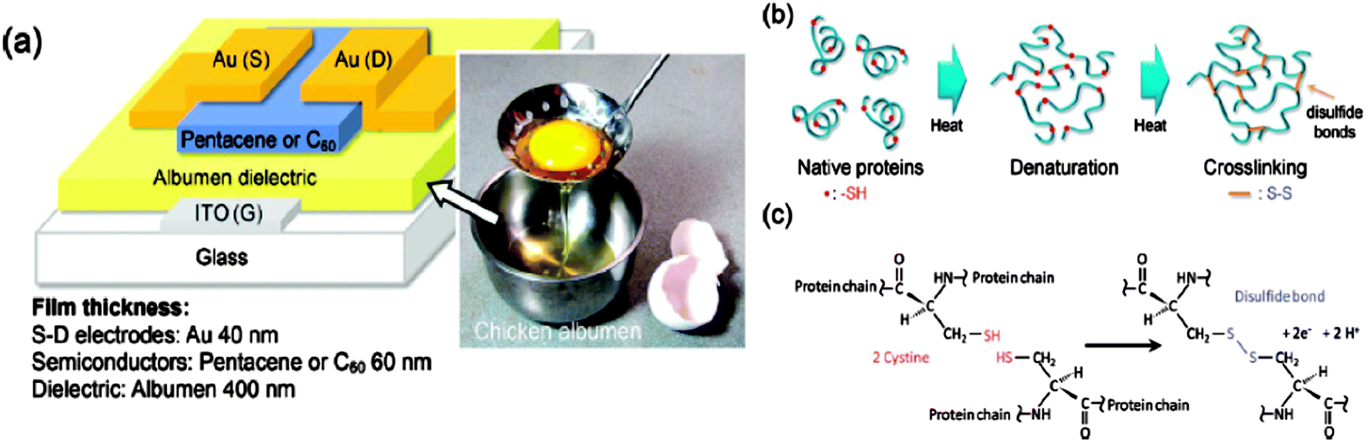 | ||
| Fig. 11 (a) Schematic of the organic field effect transistor fabricated with natural chicken albumen as the organic dielectric layer. (b) The schematic of the denaturation of albumen protein and the crosslinking reaction induced by the heat treatment temperature not exceeding 140 °C; (c) proposed crosslinking mechanism by the formation of disulfide bonds between two cysteine groups on different protein chains. Reproduced with permission from J.-W. Chang, C.-G. Wang, C.-Y. Huang, T.-D. Tsai, T.-F. Guo, and T.-C. Wen, Chicken Albumen Dielectrics in Organic Field-Effect-Transistors, Adv. Mater., 2011, 23, 4077–4081. Copyright Wiley-VCH Verlag GmbH & Co. KGaA. | ||
Synthetic organic semiconductors, a topic carefully revisited in an extensive article by Zhenan Bao's research group,7 remain the core elements of organic electronic devices (OFETs, OLEDs, OPVs, photodetectors, etc.). The organic semiconductors are receiving nowadays increasing prominence in the field of OLED display, the only real presence of organic semiconductors in large scale electronics production worldwide. Nevertheless the low charge mobility and air stability of organic semiconductors remain the two (key) limiting factors in delivering high performance for organic electronic devices comparable to their inorganic counterparts based on silicon or gallium arsenide for OPV and OFET applications.7–9
Among many possible explanations that may account for their low performance, one could be that the synthetic organic semiconductors are poorly linked to one another through weak van der Waals forces, displaying a low degree of ordering that is reflected in their rather poor air stability and limited charge transport performance compared to covalently bonded inorganic semiconductors. Nature may help mitigating this problem since it relies on air stable organic molecules that despite a lack of intramolecular π-conjugation are coupled to one another through much stronger intermolecular driven hydrogen bonding forces (e.g. DNA, cellulose, various flower and animal pigments, etc.).
Melanin is among a series of natural molecules that afford extensive H-bonding, with the first report suggesting that melanin behaves as an amorphous semiconductor threshold switch dating back to the mid-1970s (ref. 66 and references cited therein). What has baffled the researchers over the last forty years was the importance of hydration in providing good transport properties of melanin, since the scrupulous drying of the semiconducting film resulted in the disappearance of electrical conductivity. As a direct consequence, the amorphous semiconductor model became the accepted methodology over years set forth to explain the intriguing electronic and broad optical absorption properties of melanin. In a recent important contribution, the research group of Paul Meredith used muon spin relaxation spectroscopy to examine the possible role of proton mobility in the conduction of melanin as well as to observe the bound electronic spins of melanin. The group showed that in fact the hydration-dependent ionic conductivity plays a dominant role in melanin conductivity, and that the long time accepted model of melanin as an amorphous organic semiconductor is incorrect.66 In the presence of water, free carriers are produced from the comproportionation reaction, leading to the production of extrinsic free radicals (electrons) and hydronium ions (protons). Interestingly, the work of Paul Meredith's group opens wide the door for a new era of melanin bioelectronics. Specifically, their demonstration stimulates a range of new fundamentals aiming at (i) elucidating the kinetic mechanism of proton transfer reaction in melanin (with the possible existence of efficient excited state proton transfer mediating nonradiative relaxation); (ii) manipulating the comproportionation equilibrium and therefore the “doping”; and finally (iii) the unambiguous demonstration of the existence of the hybrid ionic-electronic transport mechanism in melanin recommends melanin as a fascinating candidate for bioelectronics interfacing, e.g. neuronal cell coupling, a topic that has been recently only briefly investigated.67
Indigo and other indigoids like Tyrian purple (6-6′-Br-indigo) and epindolidione in particular as well as other H-bonded dyes and pigments (i.e. anthraquinones, acridones) in general are nothing but a paradigm shift in molecular electronics design, with their application in organic electronics pioneered by the author of this article together with the research teams of Serdar Sariciftci and Siegfried Bauer. Indigo dyes are known for millennia to have been used as dyes in textiles, with blue (indigo-of plant origin) and purple (Tyrian purple-of animal origin) being the only such hue pigments until the rise of the modern era of synthetic chemistry. These molecules, together with other H-bonded molecules of natural origin (acridones, anthraquinones and naphthoquinones), display striking similarities in the type of bonding and long range order, and show higher stability to degradation by heat or chemical oxidation/reduction. Specifically, these molecules owe their remarkable properties (including color) to the existence of hydrogen bonding, which occurs both intramolecularly (and contributes to their high planarity) as well as intermolecularly (and contributes to their long range order and effective charge delocalization and transport). The discovery of semiconducting behavior in indigo57 and Tyrian purple68,69 is remarkable, considering that these molecules are known since the origin of modern civilization more than 4000 years ago, and indigo represented in the late 1800s one of the major achievements of chemical/dye industry, responsible for the rise of the chemical giant BASF. Indigo molecule was considered in the modern organic electronics era that started with the discovery of conducting polymers by MacDiarmind, Shirikawa and Heeger. However the misconception that suitable building blocks for semiconductor design should feature the intramolecularly π-conjugated core turned indigo into a non-interesting molecule for charge transport studies. Owing to their reversible two-electron reduction and oxidation and their low band gap of 1.7–1.8 eV, indigo and Tyrian purple, respectively, show high and almost perfectly balanced electron and hole charge transport in OFET devices (Fig. 12-top left panel). It is worth mentioning that even not fully optimized, the field effect mobility of Tyrian purple falls within one order of magnitude of the highest reported value of synthetic small molecule semiconductors employed in the organic electronics field.7 Inverters fabricated with Tyrian purple on the same gate electrode and with the same type of top contact electrodes (i.e. gold) displayed record quasi-static gains approaching 300 (Fig. 12-top right panel).69 Other H-bonded materials like epindolidione and quinacridone have also been investigated and their stability to degradation in air evaluated70 (Fig. 12-bottom left panel). The graph depicts the summary of mobility and stability data for competing p-type molecules reported so far in the field, and provides compelling evidence that the H-bonded semiconductors are building blocks that render very high performance for organic electronic devices, in spite of their lack of intramolecular conjugation. The amazing and intriguing performance of indigo, Tyrian purple, epindolidione and quinacridone can be explained on the basis of their high level of ordering, which can be expressed as “brick-in-the-wall” model; only the arrangement of quinacridone including its four polymorphs has been so far extensively studied and understood.71 The orientation anisotropy of H-bonded semiconductors is so acute that these molecules display charge transport and work as organic semiconductors for OFETs only when deposited on low energy, aliphatic dielectric surfaces like vacuum processed polyethylene and tetratetracontane (i.e. C44H90) or solution processed polystyrene or poly(butyl methacrylate), and potentially others too. The low surface energy aliphatic places the semiconductor molecules in a “standing-up” orientation with their hydrophobic end towards the hydrophobic surface, allowing for an ideal charge delocalization along the horizontally oriented π–π orbitals that extend between source and drain contacts.57,68,70
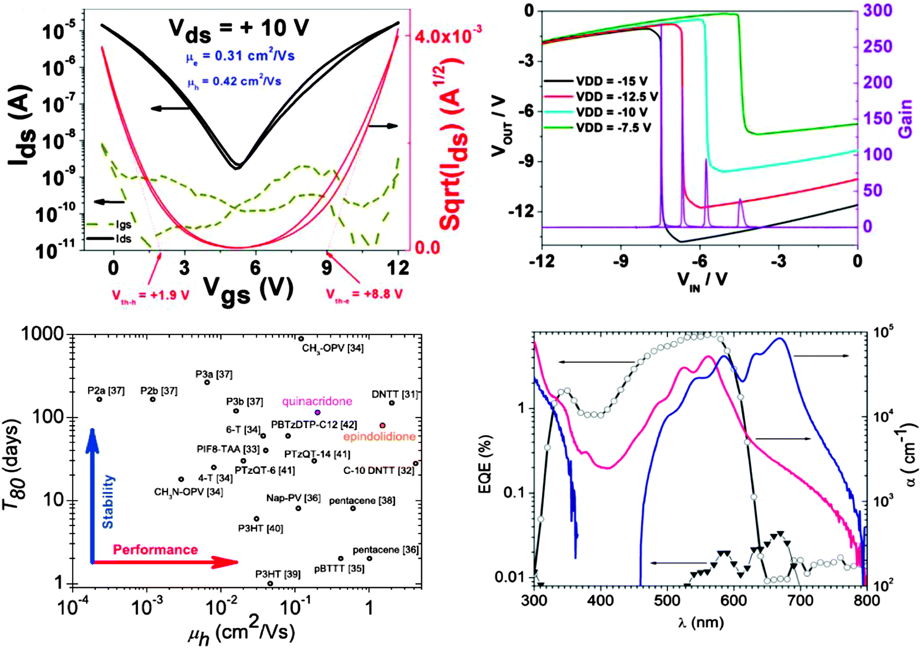 | ||
| Fig. 12 (top-left) Ambipolar field effect transistor with a Tyrian purple semiconductor and an aluminum oxide-polyethylene dielectric showing perfect balance of electron and hole transport. Reprinted from Y. Kanbur, M. Irimia-Vladu, E. D. Glowacki, G. Voss, M. Baumgartner, G. Schwabegger, L. Leonat, M. Ullah, H. Sarica, S. Erten-Ela, R. Schwodiauer, H. Sitter, Z. Kucukyavuz, S. Bauer, and N. S. Saricifci, Vacuum-processed Polyethylene as a Dielectric for Low Operating Voltage Organic Field Effect Transistors, Org. Electron., 2012, 13, 919–924. Copyright (2012), with permission from Elsevier; (top-right) quasi-static output inverter characteristics fabricated from two ambipolar transistors with the Tyrian purple channel and gold source and drain electrodes. From E. D. Glowacki, L. N. Leonat, G. Voss, M. Badea, Z. Bozkurt, M. Irimia-Vladu, S. Bauer, and N. S Sariciftci, AIP Adv., 2011, 1, 042132: used in accordance with the Creative Commons Attribution 3.0 Unported License. (bottom-left) Compilation of the reported values in the literature for p-type organic transistors plotted as stability versus field-effect mobility. Reproduced with permission from E. D. Glowacki, M. Irimia-Vladu, M. Kaltenbrunner, J. Gasiorowski, M. S. White, U. Monkowius, G. Romanazzi, G. P. Suranna, P. Mastrorilli, T. Sekitani, S. Bauer, T. Someya, L. Torsi, and N. S. Saricifci, Hydrogen-Bonded Semiconducting Pigments for Air-Stable Field-Effect Transistors, Adv. Mater., 2013, 25, 1563–1569. Copyright Wiley-VCH Verlag GmbH & Co. KGaA; (bottom-right) external quantum efficiency (EQE) of ITO-PEDOT:PSS-quinacridone-Al diodes (open circles) compared to EQE of diodes with a similar device geometry but with pentacene as the semiconductor (filled triangles). The absorption coefficient of evaporated thin films of quinacridone (pink) and pentacene (blue) is displayed on the right axis. Reprinted with permission from E. D. Glowacki, L. Leonat, M. Irimia-Vladu, R. Schwödiauer, M. Ullah, H. Sitter, S. Bauer, and N. S. Sariciftci, Intermolecular Hydrogen-bonded Organic Semiconductors—Quinacridone Versus Pentacene, Appl. Phys. Lett., 2012, 101, 023305. Copyright (2012), American Institute of Physics. | ||
Quinacridone (a low-cost synthetic derivative of naturally occurring acridone) also displays interesting photophysics properties that translate into amazingly high sensitivity to light, with the measured external quantum efficiency approaching 10% in the single layer diode configuration (i.e. the semiconductor sandwiched between two electrodes, namely ITO and aluminum). This value is more than two orders of magnitude higher than the one recorded for any other van der Waals bonded organic semiconductors (polythiophene, phthalocyanine, pentacene, etc.). A direct comparison with pentacene is presented in Fig. 12-bottom right panel.72 The single layer OPV design represents an avenue abandoned at the beginning of the 1980s when power conversion efficiencies in the range of 0.001 to 0.01% were recorded for such geometries and triggered the naissance of the actual state-of-the-art technology, i.e. the donor–acceptor model.
The work done by Serdar Sariciftci's group (ref. 72) calls for the immediate reinvestigation of the single layer organic semiconductor model for photovoltaics applications. This reconsideration is very exciting because if a larger library of H-bonded semiconductor materials, which display broader light absorption, better morphology and higher charge mobility (n.a. quinacridone has a mobility of 0.2 cm2 V s−1), will be considered, then power conversion efficiencies in the range of the values reported nowadays for top inorganic materials like silicon and gallium arsenide will be possible.
The highlighted work of the author opens a myriad of possibilities for further development and applications of H-bonded semiconductors: (i) investigate the semiconducting properties of the entire library of natural and nature-inspired (synthetically produced) molecules by the pigment/dye as well as textile and food industries; (ii) understand their film formation, processibility, morphology and polymorphism; (iii) evaluate the charge transport performance and electrochemical and photophysical characteristics; (iv) understand the mechanism of charge transport and develop modeling techniques to predict, optimize and maximize it; (v) investigate pathways to produce biotech vat dyes and pigments, in a similar fashion to the production of indigo starting from fermentation of glucose using recombinant Escherichia coli and the modified tryptophan pathway;73 (vi) perform biodegradation studies on such synthetic molecules to evaluate their level of environmental friendliness; (vii) use the gathered knowledge to fabricate novel devices, like for example: (vii.a) self-assembly monolayer–semiconductor molecules, where aliphatic chains or as mentioned above polypeptide sequences are synthetically anchored to the H-bonded semiconductor cores to generate a dielectric–semiconductor molecule in one single unit, or (vii.b) single layer organic photovoltaics; (viii) derivatize such H-bonded molecules for bio-interfacing applications, taking advantage of their suitable functional groups (i.e. amine, carbonyl) for a plethora of such derivatization reactions, to explore these molecules as building blocks for neural interfacing74 as well as (ix) many more still unfathomed applications and implications of H-bonded molecules design and synthetic developments.
In the light of the surprising electric charge transport performance of various H-bonded semiconductors featuring no intramolecular π-conjugated core, a logical follow-up would be to reevaluate the transport mechanism in H-bonded individual nucleobases and nucleobase pairs. Although the individual nucleobases were demonstrated to be excellent dielectrics,35 including also DNA itself, the careful optimization of the preferential orientation of these molecules (in a similar fashion to indigo for example) may lead to unexpected observations that could open an entire field of DNA research. In reality the DNA exploration for various electronics and optics applications is flourishing these days, and the full magnitude of this effort has been recently reviewed.75
2. Novel device geometries for sensing and integration with living tissue
Innovative architectures have been proposed recently as a tool to interface electronics with living organisms and investigate the crowded world of biological cells. The difficulty of such integration rests in the anomalous type of transport that is characteristic of complex heterogeneous materials like biological media and polymeric networks. These types of media have the characteristic slow type of transport, with a sublinear increase of mean square displacement of particles (MSD), completely different to the classic model of single-particle diffusion that has the characteristic linear increase of MSD in time; this type of unusual transport in polymeric and biological media, including governing equations and interface conditions, has been recently reviewed.41,76 To make matters more complicated for the electronic device designer, this slow and anomalous transport has to be coupled with fast and predictable electronic transport in the electronic circuit. Although the mechanism of biological and chemical sensing by organic electronic devices has been recently reviewed,42 the following subchapters will highlight some of the important contributions in the field that alleviated such coupling difficulties.2.1 Organic field-effect transistors (OFETs), organic electrochemical transistors (OECTs) and proton transistors
In the early stages of research, researchers tried first to adapt the electronic device structures to the world of biological media governed by both electronic and ionic motion. One such successful demonstration was accomplished by Zhenan Bao's research group that used water stable OFETs for sensing applications.77 Employing a cross-linked polymer gate dielectric (polyvinyl phenol), and using either pentacene or 5,5-bis-(7-dodecyl-9H-fluoren-2-yl)-2,2-bithiophene (DDFTTF) for the p-channel semiconductor, the fabricated devices displayed remarkable stability to operation in aqueous media without encapsulation, exceeding 104 cycles. Moreover the semiconductors showed sensitivity as low as parts per billion to various alcoholic analytes based on the sensing mechanism working in a similar manner to vapor detection: the small analyte or ions of interest diffuse at the dielectric/semiconductor interface and influence the charge transport in the semiconductor channel. Nevertheless, bare (non-functionalized) OFETs have no specificity to the analyte, their responses being governed by weak and nonspecific van der Waals interaction. Selectivity of field effect transistors can be achieved by incorporating receptor molecules at different positions in the device structure and relying on these receptors to selectively bind to analytes of interest and consequently modify/alter the electric signal of the device. By doing so, the direct, label-free detection (bio-recognition) of analyte of interest will offer the alternative of miniaturization and fast processing of recorded data. Typical geometries derived from the classic OFETs to be employed for detection and signal transduction in the biological world (OFET bio-sensors) are presented in Fig. 13, together with insight into operation principles, selectivity and range of detection.78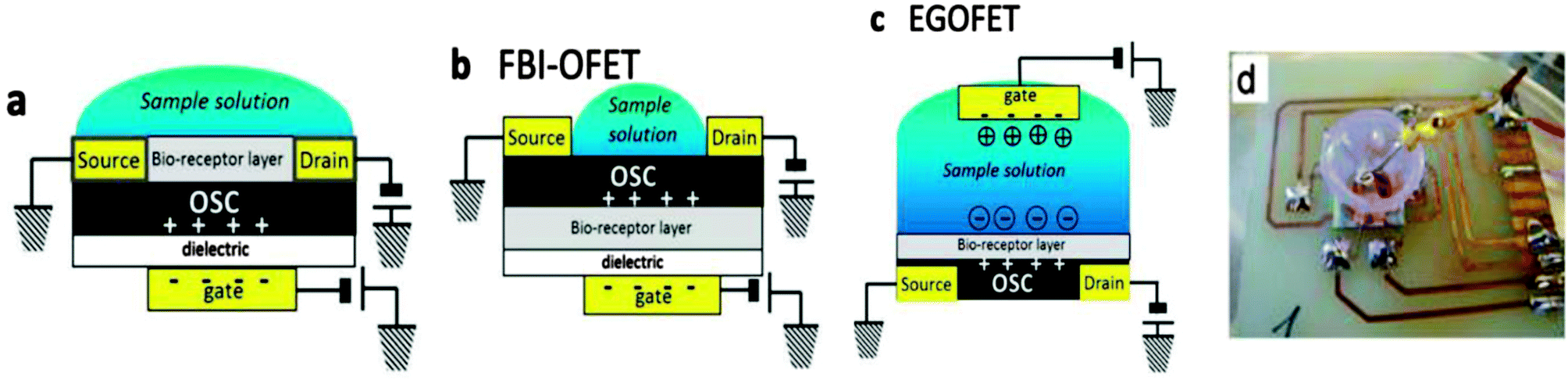 | ||
| Fig. 13 Typical architectures employed in OFET biosensors: (a) bi-layer structure (dielectric–semiconductor) with receptors anchored at the semiconductor surface and exposed to the aqueous sample containing the analyte; (b) functional bio-interlayer structure (FBI) with the receptor in the semiconductor channel, at the interface of semiconductor/dielectric; (c) organic electrochemical transistor (OECT) and EGOFET (electrolyte gated OFET), both having similar geometries but subtle different operation principles. The bio-receptor layer is placed on top of the semiconductor channel. Reproduced with permission from M. Magliulo, A. Mallardi, M. Y. Mulla, S. Cotrone, B. R. Pistillo, P. Favia, I. Vikholm-Lundin, G. Palazzo, and L. Torsi, Electrolyte-Gated Organic Field-Effect Transistor Sensors Based on Supported Biotinylated Phospholipid Bilayer, Adv. Mater., 2013, 25, 2090–2094. Copyright Wiley-VCH Verlag GmbH & Co. KGaA; (d) pictogram of the pentacene based OECT used for neural stem cell monitoring. Reproduced with permission from ref. 79 with permission from the PCCP Owner Societies. | ||
The research group of Luisa Torsi used an EGOFET geometry device (similar to the one depicted in Fig. 13c), by anchoring a functionalized bio-layer at the semiconductor interface able to control ion diffusion into the semiconductor. The device was used to establish label-free electronic sensing in an electrolyte solution having physiologically relevant ionic strength. Taking advantage of the fact that the channel/electrolyte interface in OECTs constitutes an integral part of the operation mechanism of the device, their work opens wider perspectives of translating the principle to bind any other receptors like antibodies and proteins to fluid phospholipid bilayers supported on solid surfaces and to detect the target molecules in real fluid media. The group of Fabio Biscarini used OECT geometry with the pentacene semiconductor for extracellular interfacing (stimulation, recording and differentiation) of the electric activity of stem cell-derived neuronal networks79 (Fig. 13d). Remarkably, the devices displayed selectivity and sensitivity in stem cell culture media for up to nine days, which proves that these kinds of devices can be successfully employed also for stem cell-based therapies, like for example regeneration.
In a follow-up article of their initial report on electrochemical polymerization of PEDOT:PSS, biocompatible and highly flexible/conformable, sacrificial parylene substrate of only 4 μm thickness,62 the group of George Malliaras demonstrated for the first time the extraordinary performance of OECTs for in vivo recording of brain activity in rats.80 A photograph of the device and the schematic of electric circuit are presented in Fig. 14. Their results have been made possible by the privileged geometry of OECTs versus typical OFETs that allow for a rapid integration with highly conformable substrates. The data recorded by these fully biocompatible implanted devices were validated against the measurement values of penetrating and surface electrodes respectively. Interestingly, the signal recorded by the implantable OECT devices showed superior quality, in the sense of displaying a higher signal to noise ratio and better defined peaks as compared to surface electrodes (Fig. 14-bottom). The latter report represents a major breakthrough in the field of neuronal activity recording, particularly important for applications like epileptic monitoring where it is critically important to identify zones generating high-frequency oscillations or microseizures.
 | ||
| Fig. 14 Structure and photograph of an electrocorticography (ECoG) probe made out of organic electrochemical transistors that can be conformably attached to a curvilinear surface. When implanted on the somatosensory cortex of rat brain, the transistor array was used to record the bicuculline-induced epileptic spike wave. The bottom graph shows that the implantable transistor recordings were of higher fidelity (pink type) compared to those of surface electrodes (blue type) or penetrating probes (black type). Reprinted with permission from Macmillan Publishers Ltd: D. Khodagholy, T. Doublet, P. Quilichini, M. Gurfinkel, P. Leleux, A. Ghestem, E. Ismailova, T. Herve, S. Sanaur, C. Bernard, and G. G. Malliaras. In Vivo Recordings of Brain Activity Using Organic Transistors, Nat. Commun., 2013, 4, 575. Copyright (2013). | ||
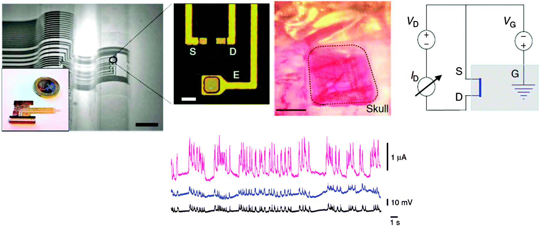
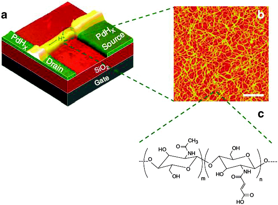
A major contribution to the field of bioelectronics was provided by the research group of Marco Rolandi that demonstrated for the first time the organic field effect transistor based on proton charge transport.81 The group employed the maleic-chitosan proton conducting layer as the organic semiconductor. The flow of protons is controlled by an electrostatic potential applied to the gate electrode that makes them dissociate from the maleic acid groups and move along the hydrated hydrogen-bonded matrix to the proton conductors PdHx protodes (not electrodes!, Fig. 15). The recorded field-effect proton mobility was μH+ ∼ 4.9 × 10⁻³ cm2 V s−1 demonstrating that with further optimization such devices could be coupled with traditional electron conducting devices and interfaced with living tissue for a wide range of applications.
 | ||
| Fig. 15 (a) Schematic and (b) atomic force micrograph of protonic field-effect transistors containing a silicon dioxide dielectric, palladium hydroxide source and drain contacts and a maleic–chitosan proton conducting layer (with chemical formula presented in panel (c)). The device works on the principle of electrostatic gate control of the maleic–chitosan proton density and the conductivity of the channel when an external voltage is applied to the gate. Reprinted with permission from Macmillan Publishers Ltd: C. Zhong, Y. Deng, A. F. Roudsari, A. Kapetanovic, M. P. Anantram, and M. Rolandi, A Polysaccharide Bioprotonic Field-effect Transistor, Nat. Commun., 2011, 2, 476. Copyright (2011). | ||
2.2 Ion bipolar junction transistors (IBJTs) and organic electronic ion pumps (OEIPs)
A major breakthrough in the establishment of ionic-based logic circuits was represented by the recent report of Magnus Berggren group, which demonstrated through a series of publications (see ref. 32 and references cited therein) the feasibility of logic gates based on a novel type of ion transistors (IBJTs – ion bipolar junction transistors). Conceptually, IBJTs are built from patterned films that have anchored fixed ionic groups and consequently display either cation or anion selectivity, according to the desired type of ion transport. An ion bipolar junction transistor is formed when two junctions of the same type (either anion or cation selective) are connected through a neutral electrolyte to a third junction of the opposite type (cation or anion selective respectively). The two junctions of the same type are denominated as emitter (E) and collector (C), whereas the dissimilar type junction is called base (B). The two possible devices that can be fabricated are the npn-type which conducts anions and the pnp-type which transports cations. In their report, the group employed both types of ionic devices in a tandem configuration to achieve the complementary functions of inverters and logic circuits normally achieved by connecting electronic-type field effect transistors that transport electrons and holes (Fig. 16). This demonstration is remarkable since it represents the first evidence of logic gates activated by means of operation of non-electronic currents. Although the switching speed of the inverter is still low (in the range of ∼100 seconds), it leaves plenty of room for ion transport optimization by carefully selecting the terminal materials as well as adjusting the concentration gradients. An outstanding demonstration of an electronic device capable of precisely delivering neurotransmitters and modulating the hearing function was provided by the group of Magnus Berggren through the aid of an innovative device, i.e. the organic electronic ion pump (OEIP;Fig. 17-left).82 The device consists of two reservoirs containing specific molecules of interest, denominated as source (S) and target (T). Each reservoir is built on top of its own PEDOT:PSS conducting pad and is separated by an overoxidized PEDOT:PSS channel that acts as an ionic but not as an electronic conductor. When an external potential is applied between the two pads in the external circuit, the electric current is balanced by an ionic current in the channel separating the S and T reservoirs. The established ionic current pumps ions that are electrophoretically transported from the source to the target reservoir in a very precise and controllable manner dictated by the external circuit potential. This technology allowed for a precise control of the delivery of neurotransmitters glutamate, aspartate and γ-amino butyric acid in an in vivo implant in the diffusive port of cochlea in rats (Fig. 17-center and right). This work is first of a kind in proving the feasibility of precise control through pulsed as opposed to continuous delivery of neurotransmitters in living tissue, and shows impressive potential for further development of therapeutic platforms. | ||
| Fig. 16 Schematic of ion bipolar junction transistors. (red frame-a) npn-IBJT where anions originate from the emitter (E), diffuse over the junction (J) and continue to the collector (C). The cationic current through the base controls the concentration of the salt in the junction and consequently the diffusion rate of anions from E to C. The emitter and collector regions are made of a similar material (crosslinked polycation), whereas the base consists of a crosslinked polyanion; (red frame-b) pnp-IBJT, where the regions and their functionality are a mirror image of the npn-IBJT: the cations are transported between E and C terminals, and anions are transported through the base; (green frame) NAND logic gates based on IBJTs: (a) npn type NAND gate consisting of two npn-IBJTs and one large resistor connected in series; (b) complementary NAND gate (CNAND) consisting of serial connection of two npn-IBJTs connected in series and two pnp-IBJTs connected in parallel; (c) and (d) the responses of the NAND and CNAND gates to the four possible combinations of input (VA, VB). Reprinted with permission from Macmillan Publishers Ltd: K. Tybrandt, R. Forchheimer, and M. Berggren, Logic Gates Based on Ion Transistors, Nat. Commun., 2012, 3, 871. Copyright (2012). | ||
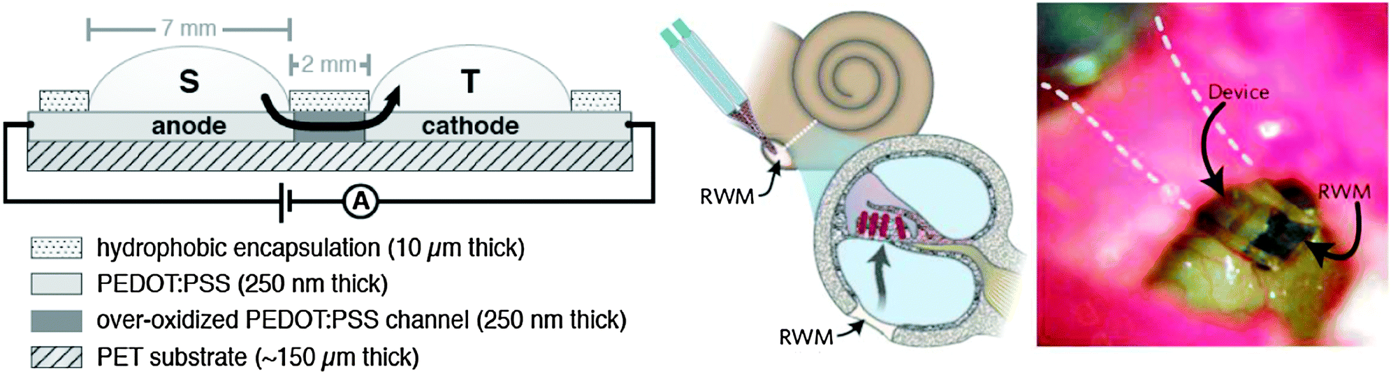 | ||
| Fig. 17 Schematic of the side view of an organic electronic ion pump. The flow of the neurotransmitters (represented by the direction of the black arrow) originates from the source reservoir (S), continues through the anode and along the overoxidized channel, until it finally reaches the cathode and the target reservoir (T). A syringe-like encapsulated OEIP device was used to in vivo modulate mammalian sensory function by precise delivery of neurotransmitters in the cochlea area (round window membrane, RWM) of the guinea pig. Reprinted with permission from Macmillan Publishers Ltd: D. T. Simon, S. Kurup, K. C. Larsson, R. Hori, K. Tybrandt, M. Goiny, E. W. H. Jager, M. Berggren, B. Canlon, and A. Richter-Dahlfors, Organic Electronics for Precise Delivery of Neurotransmitters to Modulate Mammalian Sensory Function, Nat. Mater., 2009, 8, 742–746. Copyright (2009). | ||
3. Conclusions
The work highlighted here represents just the tip of the “green” iceberg floating on the organic electronics ocean. The past ten years have witnessed a resurgence of the topic of natural materials and benign technologies for various applications, including electronics, photonics, biomedical engineering and biomimetics. The word “green” became a fashionable link to any advancement in the direction of achieving sustainability in the electronics field, although in many cases it appeared just a loose bound between the two concepts. I asked once a senior scientist during a conference break if the vat dyes are considered “green” materials – especially since most of them do not have yet a demonstrated biodegradation route (see footnote†). I was surprised to hear the answer: “Sure they are green, just dump them in the environment and Mother Nature will take care of them, in one hundred or even one thousand years; inorganics and ceramics are not green, because they stay there forever – for hundreds of thousands or million years”. Indeed, a simple inspection of Fig. 1 and the analysis of Table 1 tell us that some materials and technologies are definitely “greener” than others. However, if our ancestors had been more technologically advanced, we would have certainly not likely to experience a pile of electronics reminiscent of the Roman Empire just getting rotten in our backyard. Then what is truly green after all? Although this definition is up to debate, the author's opinion is that a truly green technology is only the one that falls into the definition of the United Nation World Commission on Environment and Development (page 37 of ref. 5). At present times, we bear the responsibility for the shape and type of environment our future generations will live in; they cannot vote now for the world we are setting up for them, and electronics are an indispensable part of our life, both in present – for us – and in future – for our forthcoming generations. The natural and nature inspired materials allow for “green” technologies that seem perfectly suited for achieving the sustainability goals in the electronics field: they embody low energy and have biodegradability and biocompatibility as their backbone features. “Green” organic electronics have already made their science debut; we just have to imagine the possibilities.Acknowledgements
The author gratefully acknowledges the mentorship and support of Prof. Serdar Sariciftci (LIOS) and Prof. Siegfried Bauer (SOMAP) at the JKU Linz. Financial support by the FWF within the framework of Austrian Science Network, NFN (Projects P20772-N20, S09712-N08 and S09711-N08), and Wittgenstein Prize of Prof. Serdar Sariciftci is gratefully acknowledged. This work was partially supported by the ERC Advanced Grant SoftMap of Prof. Siegfried Bauer as well as by the PLATE project of Joanneum Research Forschungsgesselschaft mbH. Special collaboration with Eric Glowacki, Gundula Voss, Helmut Sitter, Pavel Troshin, Luisa Torsi and Gian Paolo Suranna is gratefully acknowledged. The author thanks Prof. Jeffrey W. Fergus for proof reading the manuscript.References
- T. G. Gutowski, M. S. Branham, J. B. Dahmus, A. J. Jones, A. Thiriez and D. P. Sekulic, Thermodynamic Analysis of Resources Used in Manufacturing Processes, Environ. Sci. Technol., 2009, 43, 1584–1590 CrossRef CAS.
- J. M. Allwood, M. F. Ashby, T. G. Gutowski and E. Worrell, Material Efficiency: A White Paper, Resour., Conserv. Recycl., 2011, 55, 362–381 CrossRef PubMed.
- E. D. William, Revisiting Energy Used to Manufacture a Desktop Computer: Hybrid Analysis Combining Process and Economic Input-output Methods, IEEE Int. Symp. Electr. Environ, 2004, 0-7803-8250-1/04.
- B. C. J. Zoeteman, H. R. Krikke and J. Venselaar, Handling WEEE Waste Flows: On the Effectiveness of Producer Responsibility in a Globalizing World, Int. J. Adv. Manuf. Technol., 2010, 47, 415–436 CrossRef PubMed.
- United Nations, Report of the World Commission on Environment and Development (1987). “Our Common Future” Oxford University Press, Oxford, p. 37.
- H. Ma, O. Acton, D. O. Hutchins, N. Cernetic and A. K.-Y. Jen, Multifunctional Phosphonic Acid Self-assembled Monolayers on Metal Oxides as Dielectrics, Interface Modification Layers and Semiconductors for Low-voltage High-performance Organic Field-effect Transistors, Phys. Chem. Chem. Phys., 2012, 14, 14110–14126 RSC.
- J. Mei, Y. Diao, A. L. Appleton, L. Fang and Z. Bao, Integrated Materials Design of Organic Semiconductors for Field-Effect Transistors, J. Am. Chem. Soc., 2013, 135, 6724–6746 CrossRef CAS PubMed.
- R. A. Jenssen and J. Nelsson, Factors Limiting Device Efficiency in Organic Photovoltaics, Adv. Mater., 2013, 25, 1847–1858 CrossRef PubMed.
- M. Jørgensen, K. Norrman, S. A. Gevorgyan, T. Tromholt, B. Andreasen and F. C. Krebs, Stability of Polymer Solar Cells, Adv. Mater., 2012, 24, 580–612 CrossRef PubMed.
- F. Ante, D. Kälblein, T. Zaki, U. Zschieschang, K. Takimiya, M. Ikeda, T. Sekitani, T. Someya, J. N. Burghartz, K. Kern and H. Klauk, Contact Resistance and Megahertz Operation of Aggressively Scaled Organic Transistors, Small, 2012, 8, 73–79 CrossRef CAS PubMed.
- M. Kaltenbrunner, M. S. White, E. D. Głowacki, T. Sekitani, T. Someya, N. S. Sariciftci and S. Bauer, Ultrathin and Lightweight Organic Solar Cells with High Flexibility, Nat. Commun., 2012, 3, 770 CrossRef PubMed.
- R. M. Owens and G. G. Malliaras, Organic Electronics at the Interface with Biology, Mater. Today, 2010, 35, 449–456 CAS.
- T. Sekitani and T. Someya, Human-friendly Organic Integrated Circuits, Mater. Today, 2011, 14, 398–407 CrossRef CAS.
- G. M. Whitesides, The Frugal Way, The Economist - The World in 2012, 2011.
- S. Y. Reece, J. A. Hamel, K. Sung, T. D. Jarvi, A. J. Esswein, J. J. H. Pijpers and D. G. Nocera, Wireless Solar Water Splitting Using Silicon-based Semiconductors and Earth-abundant Catalysts, Science, 2011, 334, 645–648 CrossRef CAS PubMed.
- K.-H. Jeong, J. Kim and L. P. Lee, Biologically Inspired Artificial Compound Eyes, Science, 2006, 312, 557–561 CrossRef CAS PubMed.
- M. Kolle, A. Lethbridge, M. Kreysing, J. J. Baumberg, J. Aizenberg and P. Vukusic, Bio-Inspired Band-Gap Tunable Elastic Optical Multilayer Fibers, Adv. Mater., 2013, 25, 2239–2245 CrossRef CAS PubMed.
- H. Hosseinkhan, P.-D. Hong and D.-S. Yu, Self-Assembled Proteins and Peptides for Regenerative Medicine, Chem. Rev., 2013, 113, 4837–4861 CrossRef PubMed.
- H. Ma, M. T. Zin, M. H. Zareie, M. S. Kang, S.-H. Kang, K.-S. Kim, B. W. Reed, C. Tamerler Behar, M. Sarikaya and A. K.-Y. Jen, Assembly of Nanomaterials Through Highly Ordered Self-assembled Monolayers and Peptide-organic Hybrid Conjugates as Templates, J. Nanosci. Nanotechnol., 2007, 7, 2549–2566 CrossRef CAS PubMed.
- A. Ressine, G. Marko-Varga and T. Laurell, Porous Silicon Protein Microarray Technology and Ultra-superhydrophobic States for Improved Bioanalytical Readout, Biotechnol. Annu. Rev., 2007, 13, 149–200 CrossRef CAS.
- T. Endlein, A. Ji, D. Samuel, N. Yao, Z. Wang, W. J. P. Barnes, W. Federle, M. Kappl and Z. Dai, Sticking Like Sticky Tape: Tree Frogs use Friction Forces to Enhance Attachment on Overhanging Surfaces, J. R. Soc. Interface, 2013, 10, 20120838 CrossRef PubMed.
- B. J. Blaiszik, S. L. B. Kramer, S. C. Olugebefola, J. S. Moore, N. R. Sottos and S. R. White, Self-healing Polymers and Composites, Annu. Rev. Mater. Res., 2010, 40, 179–211 CrossRef CAS.
- L. Phan, W. G. Walkup IV, D. D. Ordinario, E. Karshalev, J.-M. Jocson, A. M. Burke and A. A. Gorodetsky, Reconfigurable Infrared Camouflage Coatings from a Cephalopod Protein, Adv. Mater., 2013 DOI:10.1002/adma.201301472.
- V. Magdanz, S. Sanchez and O. G. Schmidt, Development of a Sperm-Flagella Driven Micro-Bio-Robot, Adv. Mater., 2013 DOI:10.1002/adma.201302544.
- F. G. Omenetto and D. Kaplan, New Opportunities for an Ancient Material, Science, 2010, 329, 528–531 CrossRef CAS PubMed.
- P. Meredith, C. J. Bettinger, M. Irimia-Vladu, A. B. Mosert and P. Schwenn, Electronic and Optoelectronic Materials and Devices Inspired by Nature, Rep. Prog. Phys., 2013, 76, 034501 CrossRef CAS PubMed.
- W. Suginta, P. Khunkaewla and A. Schulte, Electrochemical Biosensor Applications of Polysaccharides Chitin and Chitosan, Chem. Rev., 2013, 113, 5458–5479 CrossRef CAS PubMed.
- M. Berggren and A. Richter-Dahlfors, Organic Bioelectronics, Adv. Mater., 2007, 19, 3201–3213 CrossRef CAS.
- D. H. Kim, N. Lu, R. Ma, Y. S. Kim, R. H. Kim, S. Wang, J. Wu, S. M. Won, H. Tao, A. Islam, K. J. Yu, T. Kim, R. Chowdhury, M. Ying, L. Xu, M. Li, H. J. Chung, H. Keum, M. McCormick, P. Liu, Y. W. Zhang, F. G. Omenetto, Y. Huang, T. Coleman and J. A. Rogers, Epidermal Electronics, Science, 2011, 333, 838–843 CrossRef CAS PubMed.
- D. Martin, Organic Electronics: Polymers Manipulate Cells, Nat. Mater., 2007, 6, 626–627 CrossRef CAS PubMed.
- N. R. Pollock, J. P. Rolland, S. Kumar, P. D. Beattie, S. Jain, F. Noubary, V. L. Wong, R. A. Pohlmann, U. S. Ryan and G. M. Whitesides, A Paper-Based Multiplexed Transaminase Test for Low-Cost, Point-of-Care Liver Function Testing, Sci. Transl. Med., 2012, 4, 152ra129 CrossRef PubMed.
- K. Tybrandt, R. Forchheimer and M. Berggren, Logic Gates Based on Ion Transistors, Nat. Commun., 2012, 3, 871 CrossRef PubMed.
- R. V. Martinez, J. L. Branch, C. R. Fish, L. Jin, R. F. Shepherd, R. M. D. Nunes, Z. Suo and G. M. Whitesides, Robotic Tentacles with Three-Dimensional Mobility Based on Flexible Elastomers, Adv. Mater., 2013, 25, 205–212 CrossRef CAS PubMed.
- C. J. Bettinger and Z. Bao, Organic Thin-Film Transistors Fabricated on Resorbable Biomaterial Substrates, Adv. Mater., 2010, 22, 651–655 CrossRef CAS PubMed.
- M. Irimia-Vladu, P. A. Troshin, M. Reisinger, L. Shmygleva, Y. Kanbur, G. Schwabegger, M. Bodea, R. Schwödiauer, A. Mumyatov, J. W. Fergus, V. Razumov, H. Sitter, N. S. Sariciftci and S. Bauer, Biocompatible and Biodegradable Materials for Organic Field-Effect Transistors, Adv. Funct. Mater., 2010, 20, 4069–4076 CrossRef CAS.
- H. Tao, M. A. Brenckle, M. Yang, J. Zhang, M. Liu, S. M. Siebert, R. D. Averitt, M. S. Mannoor, M. C. McAlpine, J. A. Rogers, D. L. Kaplan and F. G. Omenetto, Silk-Based Conformal, Adhesive, Edible Food Sensors, Adv. Mater., 2012, 24, 1067–1072 CrossRef CAS PubMed.
- D. Tobjörk and R. Österbacka, Paper Electronics, Adv. Mater., 2011, 23, 1935–1961 CrossRef PubMed.
- M. D. Angione, R. Pilolli, S. Cotrone, M. Magliulo, A. Mallardi, G. Palazzo, L. Sabbatini, D. Fine, A. Dodabalapur, N. Cioffi and L. Torsi, Carbon Based Materials for Electronic Bio-sensing, Mater. Today, 2011, 14, 424–433 CrossRef CAS.
- K. Svennersten, K. C. Larsson, M. Berggren and A. Richter-Dahlfors, Organic Bioelectronics in Nanomedicine, Biochim. Biophys. Acta, 2011, 1810, 276–285 CrossRef CAS PubMed.
- M. Muskovich and C. J. Bettinger, Biomaterials-Based Electronics: Polymers and Interfaces for Biology and Medicine, Adv. Healthcare Mater., 2012, 1, 248–266 CrossRef CAS PubMed.
- B. Chertok, M. J. Webber, M. D. Succi and R. Langer, Drug Delivery Interfaces in the 21st Century: From Science Fiction Ideas to Viable Technologies, Mol. Pharmaceutics, 2013, 10, 3531–3543 CAS.
- L. Torsi, M. Magliulo, K. Manoli and G. Palazzo, Organic Field-effect Transistor Sensors: A Tutorial Review, Chem. Soc. Rev., 2013 10.1039/c3cs60127g.
- J. A. Lewis, Material Challenge for Flexible Organic Devices-Permeation Barrier for Encapsulate Layers, Mater. Today, 2006, 9, 38–45 CrossRef CAS.
- L. Nyholm, G. V. Nyström, A. Mihranyan and M. Strømme, Toward Flexible Polymer and Paper-Based Energy Storage Devices, Adv. Mater., 2011, 23, 3751–3769 CAS.
- L. Hu, J. W. Choi, Y. Yang, S. Jeong, F. La Mantia, L. F. Cui and Y. Cui, Highly Conductive Paper for Energy-storage Devices, Proc. Natl. Acad. Sci. U. S. A., 2009, 106, 21490–21494 CrossRef CAS PubMed.
- D. Y. Kim and A. J. Steckl, Electrowetting on Paper for Electronic Paper Display, ACS Appl. Mater. Interfaces, 2010, 2, 3318–3323 CAS.
- U. Zschieschang, T. Yamamoto, K. Takimiya, H. Kuwabara, M. Ikeda, T. Sekitani, T. Someya and H. Klauk, Organic Electronics on Banknotes, Adv. Mater., 2011, 23, 654–658 CrossRef CAS PubMed.
- M. C. Barr, J. A. Rowehl, R. R. Lunt, J. Xu, A. Wang, C. M. Boyce, S. G. Im, V. Bulovic and K. K. Gleason, Direct Monolithic Integration of Organic Photovoltaic Circuits on Unmodified Paper, Adv. Mater., 2011, 23, 3500–3505 CrossRef CAS PubMed.
- M. C. Belanger and Y. Marois, Homocompatibility, Biocompatibility, Inflammatory and In vivo Studies of Primary Reference Materials Low-density Polyethylene and Polydimethylsiloxane: A Review, J. Biomed. Mater. Res., 2001, 58, 567–577 CrossRef PubMed.
- E. Delivopoulos, D. J. Chew, I. R. Minev, J. W. Fawcett and S. P. Lacour, Concurrent Recordings of Bladder Afferents from Multiple Nerves Using a Microfabricated PDMS Microchannel Electrode Array, Lab Chip, 2012, 12, 2540–2551 RSC.
- Y. Onuki, U. Bhardwaj, F. Papadimitrakopoulos and D. J. Burgess, A Review of the Biocompatibility of Implantable Devices: Current Challenges to Overcome Foreign Body Response, J. Diabetes Sci. Technol., 2008, 2, 1003–1015 Search PubMed.
- M. C. Serrano, E. J. Chung and G. A. Ameer, Advances and Applications of Biodegradable Elastomers in Regenerative Medicine, Adv. Funct. Mater., 2010, 20, 192–208 CrossRef CAS.
- L. Zhang, Z. Cao, T. Bai, L. Carr, J.-R. Ella-Menye, C. Irvin, B. D. Ratner and S. Jiang, Zwitterionic Hydrogels Implanted in Mice Resist the Foreign-body Reaction, Nat. Biotechnol., 2013, 31, 553–556 CrossRef CAS PubMed.
- Y. J. Kim, S.-E. Chun, J. Whitacre and C. J. Bettinger, Self-deployable Current Sources Fabricated from Edible Materials, J. Mater. Chem. B, 2013, 1, 3781–3788 RSC.
- V. Benfenati, S. Toffanin, R. Capelli, L. M. A. Camassa, S. Ferroni, D. L. Kaplan, F. G. Omenetto, M. Muccini and R. Zamboni, A Silk Platform that Enables Electrophysiology and Targeted Drug Delivery in Brain Astroglial Cells, Biomaterials, 2010, 31, 7883–7891 CrossRef CAS PubMed.
- D.-H. Kim, J. Viventi, J. J. Amsden, J. Xiao, L. Vigeland, Y.-S. Kim, J. A. Blanco, B. Panilaitis, E. S. Frechette, D. Contreras, D. L. Kaplan, F. G. Omenetto, Y. Huang, K.-C. Hwang, M. R. Zakin, B. Litt and J. A. Rogers, Dissolvable Films of Silk Fibroin for Ultrathin Conformal Bio-integrated Electronics, Nat. Mater., 2010, 9, 511–517 CrossRef CAS PubMed.
- M. Irimia-Vladu, E. D. G1owacki, P. A. Troshin, G. Schwabegger, L. Leonat, D. K. Susarova, O. Krystal, M. Ullah, Y. Kanbur, M. A. Bodea, V. F. Razumov, H. Sitter, S. Bauer and N. S. Saricifci, Indigo - A Natural Pigment for High Performance Ambipolar Organic Field Effect Transistors and Circuits, Adv. Mater., 2012, 24, 375–380 CrossRef CAS PubMed.
- M. Irimia-Vladu, E. D. Głowacki, G. Schwabegger, L. Leonat, H. Z. Akpinar, H. Sitter, S. Bauer and N. S. Sariciftci, Natural Resin Shellac as a Substrate and a Dielectric Layer for Organic Field-effect Transistors, Green Chem., 2013, 15, 1473–1476 RSC.
- N. Martino, D. Ghezzi, F. Benfenati, G. Lanzani and M. R. Antognazza, Organic Semiconductors for Artificial Vision, J. Mater. Chem. B, 2013, 1, 3768–3780 RSC.
- M. Asplund, T. Nyberg and O. Inganäs, Electroactive Polymers for Neural Interfaces, Polym. Chem., 2010, 1, 1374–1391 RSC.
- S. M. Richardson-Burns, J. L. Hendricks and D. C. Martin, Electrochemical Polymerization of Conducting Polymers in Living Neural Tissue, J. Neural Eng., 2007, 4, L6–L13 CrossRef PubMed.
- D. Khodagholy, T. Doublet, M. Gurfinkel, P. Quilichini, E. Ismailova, P. Leleux, T. Herve, S. Sanaur, C. Bernard and G. G. Malliaras, Highly Conformable Conducting Polymer Electrodes for In Vivo Recordings, Adv. Mater., 2011, 23, H268–H272 CrossRef CAS PubMed.
- C. Yang, W. Lin, Z. Li, R. Zhang, H. Wen, B. Gao, G. Chen, P. Gao, M. M. F. Yuen and C. P. Wong, Water-Based Isotropically Conductive Adhesives: Towards Green and Low-Cost Flexible Electronics, Adv. Funct. Mater., 2011, 21, 4582–4588 CrossRef CAS.
- A. Dezieck, O. Acton, K. Leong, E. E. Oren, H. Ma, C. Tamerler, M. Sarikaya and A. K. Y. Jen, Threshold Voltage Control in Organic Thin Film Transistors with Dielectric Layer Modified by a Genetically Engineered Polypeptide, Appl. Phys. Lett., 2010, 97, 013307 CrossRef.
- J.-W. Chang, C.-G. Wang, C.-Y. Huang, T.-D. Tsai, T.-F. Guo and T.-C. Wen, Chicken Albumen Dielectrics in Organic Field-Effect-Transistors, Adv. Mater., 2011, 23, 4077–4081 CrossRef CAS PubMed.
- A. B. Mostert, B. J. Powell, F. L. Pratt, G. R. Hanson, T. Sarnad, I. R. Gentle and P. Meredith, Role of Semiconductivity and Ion Transport in the Electrical Conduction of Melanin, Proc. Natl. Acad. Sci. U. S. A., 2012, 109, 8943–8947 CrossRef CAS PubMed.
- C. J. Bettinger, J. P. Bruggeman, A. Misra, J. T. Borenstein and R. Langer, Biocompatibility of Biodegradable Semiconducting Melanin films for Nerve Tissue Engineering, Biomaterials, 2009, 30, 3050–3057 CrossRef CAS PubMed.
- Y. Kanbur, M. Irimia-Vladu, E. D. Glowacki, G. Voss, M. Baumgartner, G. Schwabegger, L. Leonat, M. Ullah, H. Sarica, S. Erten-Ela, R. Schwodiauer, H. Sitter, Z. Kucukyavuz, S. Bauer and N. S. Saricifci, Vacuum-processed Polyethylene as a Dielectric for Low Operating Voltage Organic Field Effect Transistors, Org. Electron., 2012, 13, 919–924 CrossRef CAS PubMed.
- E. D. Glowacki, L. N. Leonat, G. Voss, M. Badea, Z. Bozkurt, M. Irimia-Vladu, S. Bauer and N. S. Sariciftci, Ambipolar Organic Field Effect Transistors and Inverters with the Natural Material Tyrian Purple, AIP Adv., 2011, 1, 042132 CrossRef.
- E. D. Glowacki, M. Irimia-Vladu, M. Kaltenbrunner, J. Gasiorowski, M. S. White, U. Monkowius, G. Romanazzi, G. P. Suranna, P. Mastrorilli, T. Sekitani, S. Bauer, T. Someya, L. Torsi and N. S. Saricifci, Hydrogen-Bonded Semiconducting Pigments for Air-Stable Field-Effect Transistors, Adv. Mater., 2013, 25, 1563–1569 CrossRef CAS PubMed.
- G. Lincke, On Quinacridones and Their Supramolecular Mesomerism Within the Crystal Lattice, Dyes Pigm., 2002, 52, 169–181 CrossRef CAS.
- E. D. Glowacki, L. Leonat, M. Irimia-Vladu, R. Schwödiauer, M. Ullah, H. Sitter, S. Bauer and N. S. Sariciftci, Intermolecular Hydrogen-bonded Organic Semiconductors—Quinacridone Versus Pentacene, Appl. Phys. Lett., 2012, 101, 023305 CrossRef.
- A. Berry, T. C. Dodge, M. Pepsin and W. Weyler, Application of Metabolic Engineering to Improve Both the Production and Use of Biotech Indigo, J. Ind. Microbiol. Biotechnol., 2002, 28, 127–133 CrossRef CAS.
- E. Bystrenova, M. Jelitai, I. Tonazzini, A. N. Lazar, M. Huth, P. Stoliar, C. Dionigi, M. G. Cacace, B. Nickel, E. Madarasz and F. Biscarini, Neural Networks Grown on Organic Semiconductors, Adv. Funct. Mater., 2008, 18, 1751–1756 CrossRef CAS.
- Y.-W. Kwon, C. H. Lee, D.-H. Choi and J. I. Jin, Material Science of DNA, J. Mater. Chem., 2009, 19, 1353–1380 RSC.
- F. Höfling and T. Franosch, Anomalous Transport in the Crowded World of Biological Cells, Rep. Prog. Phys., 2013, 76, 046602 CrossRef PubMed.
- M. E. Roberts, S. C. B. Mannsfeld, N. Queraltó, C. Reese, J. Locklin, W. Knoll and Z. Bao, Water-stable Organic Transistors and Their Application in Chemical and Biological Sensors, Proc. Natl. Acad. Sci. U. S. A., 2008, 105, 12134–12139 CrossRef CAS PubMed.
- M. Magliulo, A. Mallardi, M. Y. Mulla, S. Cotrone, B. R. Pistillo, P. Favia, I. Vikholm-Lundin, G. Palazzo and L. Torsi, Electrolyte-Gated Organic Field-Effect Transistor Sensors Based on Supported Biotinylated Phospholipid Bilayer, Adv. Mater., 2013, 25, 2090–2094 CrossRef CAS PubMed.
- T. Cramer, B. Chelli, M. Murgia, M. Barbalinardo, E. Bystrenova, D. M. de Leeuw and F. Biscarini, Organic Ultra-thin Film Transistors With a Liquid Gate for Extracellular Stimulation and Recording of Electric Activity of Stem Cell-derived Neuronal Networks, Phys. Chem. Chem. Phys., 2013, 15, 3897–3905 RSC.
- D. Khodagholy, T. Doublet, P. Quilichini, M. Gurfinkel, P. Leleux, A. Ghestem, E. Ismailova, T. Herve, S. Sanaur, C. Bernard and G. G. Malliaras, In Vivo Recordings of Brain Activity Using Organic Transistors, Nat. Commun., 2013, 4, 575 Search PubMed.
- C. Zhong, Y. Deng, A. F. Roudsari, A. Kapetanovic, M. P. Anantram and M. Rolandi, A Polysaccharide Bioprotonic Field-effect Transistor, Nat. Commun., 2011, 2, 476 CrossRef PubMed.
- D. T. Simon, S. Kurup, K. C. Larsson, R. Hori, K. Tybrandt, M. Goiny, E. W. H. Jager, M. Berggren, B. Canlon and A. Richter-Dahlfors, Organic Electronics for Precise Delivery of Neurotransmitters to Modulate Mammalian Sensory Function, Nat. Mater., 2009, 8, 742–746 CrossRef CAS PubMed.
Footnote |
| † On-going research of the author together with the group of Fernando Bautista at King Juan Carlos Univ. Madrid showed that synthetic pigments quinacridone and epindolidione are biodegradable. The publication of such results is in progress. |
| This journal is © The Royal Society of Chemistry 2014 |