
 Open Access Article
 This Open Access Article is licensed under a
 Creative Commons Attribution 3.0 Unported Licence
Autocatalytic growth of ZnO nanorods from flat Au(111)-supported ZnO films
Leandro
Pascua
a,
Fernando
Stavale
ab,
Niklas
Nilius
*ac and
Hans-Joachim
Freund
a
aFritz-Haber-Institut der Max-Planck-Gesellschaft, Faradayweg 4-6, D-14195 Berlin, Germany
bCentro Brasileiro de Pesquisas Físicas - CBPF/MCTI, Rua Xavier Sigaud 150, 22290-180, Rio de Janeiro, Brazil
cInstitut für Physik, Carl von Ossietzky Universität Oldenburg, D-26111 Oldenburg, Germany. E-mail: niklas.nilius@uni-oldenburg.de
First published on 27th October 2014
Abstract
Physical vapour deposition of ZnO on an Au(111) support has been investigated as a function of the oxygen chemical potential by means of scanning tunnelling microscopy and luminescence spectroscopy. Whereas a layer-by-layer growth of ZnO is revealed in oxygen excess, formation of oxide nanorods with large height-to-diameter ratio prevails at lower oxygen chemical potentials. We ascribe the formation of 3D nanostructures in the latter case to traces of Au atoms on the surface that promote trapping and dissociation of the incoming oxygen molecules. The Au residuals, acting as catalyst for the oxide formation, are indeed found on top of the ZnO nanorods.
1. Introduction
Zinc oxide (ZnO) is one of the most intensively studied oxide materials due to its unique electronic and optical behaviour, in particular its direct band gap in the UV (3.37 eV), the large exciton binding energy of 60 meV and the high electron mobility.1,2 These distinct properties make ZnO a fascinating inorganic compound for optoelectronic applications, such as solar cells, light emitting devices and transparent conductors. However, not only its spectral behaviour but also the amazing variability of structural manifestations renders this semi-conducting oxide attractive.3 In its most stable wurtzite configuration, ZnO can be grown as single crystals or crystalline films, while graphene-like structures with Zn and O ions sitting in the same plane are adopted in the limit of ultrathin layers.4 In addition, ZnO nanostructures with almost arbitrarily shapes have been synthesized, among others nanorods, nano-flowers, nanobelts, nanospirals and nanopropellers.3,5,6 These nano-materials are envisioned for a variety of applications, e.g. as optical waveguides, nanorod lasers, absorber materials for solar cells,7 light- and electron-emitters as well as active elements for heterogeneous and photo-catalysts.8 In all these applications, a high surface to volume ratio of the structures is desirable and forms the target line for optimizations.Common fabrication routes of ZnO nanostructures exploit physical and chemical approaches, such as magnetron sputtering, laser ablation and molecular beam epitaxy,1 as well as wet-chemical synthesis, metal–organic vapour-phase epitaxy,9 solvothermal,10 and electrochemical deposition,11 and vapour–liquid–solid (VLS) growth.12 The characterization of the so produced materials is often carried out by ex situ techniques, such as electron microscopy. In many cases, metal catalysts made of noble (Au and Ag)13 or transition metals (Ni, Fe and Mo) are used to accelerate the oxide growth. In the VLS technique, for example, the catalyst forms a liquid alloy droplet with zinc atoms from the gas phase that initiates and guides the growth of nanowires.14–16 The wire diameter is thereby governed by the size of the catalyst particle. In many cases, gold was identified to be the ideal growth catalyst, as it promotes the formation of ZnO nanorods with 50–100 nm diameter and up to 10 μm length.1,5
As mentioned above, ZnO nanostructures are mostly fabricated by high-throughput techniques, while surface science approaches, e.g. physical vapour deposition in an UHV environment, combined with high-end topographic and spectroscopic characterization are rarely used.17 In the few examples, scanning tunnelling (STM) and atomic force microscopy have been employed to characterize the atomic structure,18 adsorption characteristics,19 and polarity compensation schemes20 of crystalline ZnO surfaces. Moreover, homogenous oxide films were prepared and characterized at the atomic scale on a variety of metallic and dielectric substrates, such as Pd(111),21 Au(111),22 Pt(111) and Al2O3(1010).23 However, systematic growth studies of 3D oxide structures, exploiting the full arsenal of surface science methods, are hardly found in the literature. This is a somewhat unsatisfying situation, as surface science approaches provide ultraclean and highly reproducible preparation conditions for oxide nanostructures, as well as various tools for their in situ characterization. By exploiting these advantages, a deeper insight into fundamental growth properties of ZnO could be achieved that goes beyond the existing picture.1,3
In this work, we demonstrate how the ZnO growth on an Au(111) support can be switched from a layer-by-layer mode, giving rise to flat, crystalline films, to a 3D regime that leads to the development of nanorods. The latter are oriented along the surface normal and expose constant height-to-diameter ratios. We have identified the oxygen chemical potential as the crucial parameter controlling the different growth regimes. Moreover, highly resolved STM data indicate that nanorod formation is catalysed by traces of Au that accumulates on the surface of ZnO/Au(111) films at certain conditions.
2. Experimental details
All experiments have been carried out in an ultrahigh vacuum chamber (p0 = 2 × 10⁻¹⁰ mbar), equipped with a liquid-nitrogen cooled STM and standard facilities for sample preparation and analysis, e.g. low-energy-electron diffraction (LEED), an ion gun and different e-beam evaporators. Our STM has been specifically designed to collect photons from the tip–sample junction.24 For this purpose, the microscope head is placed inside of a parabolic mirror with the tip located in the focal point. The mirror collects photons from the STM junction and guides them out of the vacuum chamber towards a CCD detector attached to a grating spectrograph (150 lines per mm). The ZnO structures were prepared by sublimating ZnO pellets from an e-beam evaporator onto a sputtered and annealed Au(111) single crystal in 5 × 10⁻⁶ mbar of oxygen.22 The nominal film thickness was set to 25 ML. To ensure good crystallinity, the films were annealed for 10 min to different temperatures either in vacuum or O2 ambience. This annealing step turned out to be crucial for the dimensionality of the ZnO structures, i.e. their 2D or 3D character. The film quality was routinely checked with LEED, showing an intense, hexagonal spot pattern indicative for the {0001} termination of the wurtzite lattice (Fig. 1a, inset).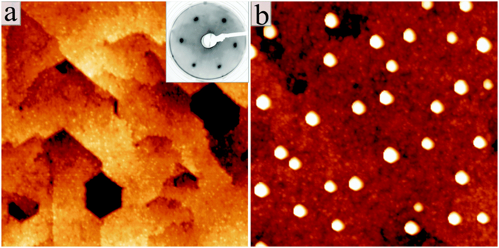 | ||
| Fig. 1 STM images of (a) flat ZnO on Au(111) and (b) a film homogenously covered with ZnO nanorods (Us = 4.0 V, 200 × 200 nm2). The inset in (a) shows a LEED pattern of the flat film taken at 100 eV electron energy. | ||
3. Results and discussion
Fig. 1 shows STM images for the two manifestations of our ZnO samples. Whereas a flat film with wide terraces of triangular or hexagonal shape is observed in (a), a nanorod-array sitting on top of a ZnO wetting layer is identified in (b). Only the final annealing step has been varied in the two preparations. While sample (a) was tempered at 700 K in 5 × 10⁻⁶ mbar of oxygen, sample (b) was vacuum-annealed at 800 K. Apparently, this variation in the annealing procedure is sufficient to induce drastic changes in the growth morphology of the oxide. Both, the ZnO wetting layer and the nanostructures are clearly of crystalline nature, as deduced from the sharp LEED pattern of the film and the distinct geometry of the nanorods, respectively. Top facets of the nanorods are always hexagonal in shape, indicating a {0001} termination similar to that of the film (Fig. 2a). The side facets are tentatively assigned to {2![[1 with combining macron]](https://www.rsc.org/images/entities/char_0031_0304.gif) 0} planes that also feature low formation energies and are often observed in ZnO nanostructures.3,6 The experimental aspect ratio (height-to-diameter) of the rods varies between 0.1 and 0.2, depending on the preparation conditions (Fig. 2b). These values are considerable smaller than for ZnO nanorods prepared by wet-chemical methods. However, the aspect ratio should be taken as a lower bound, as the rod diameter was not corrected for tip convolution effects.
0} planes that also feature low formation energies and are often observed in ZnO nanostructures.3,6 The experimental aspect ratio (height-to-diameter) of the rods varies between 0.1 and 0.2, depending on the preparation conditions (Fig. 2b). These values are considerable smaller than for ZnO nanorods prepared by wet-chemical methods. However, the aspect ratio should be taken as a lower bound, as the rod diameter was not corrected for tip convolution effects.
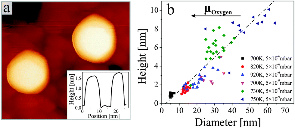 | ||
| Fig. 2 (a) Close up STM image of two nanorods on ZnO/Au(111) (4.0 V, 30 × 30 nm2). A height profile across the rods is shown in the inset. (b) Histogram of height-to-diameter ratios for nanorods produced at different preparation conditions (see symbols). The mean aspect ratio of the rods amounts to 0.15. | ||
Detailed inspection of the data reveals a direct correlation between the geometry of the ZnO nanorods and the specific annealing conditions. To enable comparability of all experiments, we introduce the oxygen chemical potential μO2, as combined parameter of O2 partial pressure p and annealing temperature T: 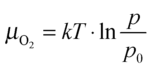 .25 Here, k is the Boltzmann constant and p0 is the atmospheric pressure. The dimensionality of the ZnO is quantified by the volume ratio between the nanorods Vrod and the absolute amount of deposited material that corresponds to 25 ML nominal thickness in all cases. The nanorod volume is estimated by measuring height and diameter of all ad-structures in a characteristic surface region (e.g. 100 × 100 nm2), treating the rods as perfect cylinders. Note that the lateral rod size was not corrected for tip convolution effects, causing Vrod to be overestimated by about 25%. However, this systematic error has no consequences on the general conclusions of our analysis that deals with relative instead of absolute trends. The dependence of the oxide dimensionality on the O2 chemical potential is summarized in the diagram shown in Fig. 3. Apparently, the nanorod contribution to the total film volume continuously increases with decreasing O2 chemical potential. Whereas flat ZnO films develop on Au(111) at low-temperature and/or oxygen-rich annealing conditions, pronounced 3D structures are formed upon high-temperature annealing in an O2-poor environment. A selection of ZnO preparations visualizing this trend is depicted in Fig. 3 as well.
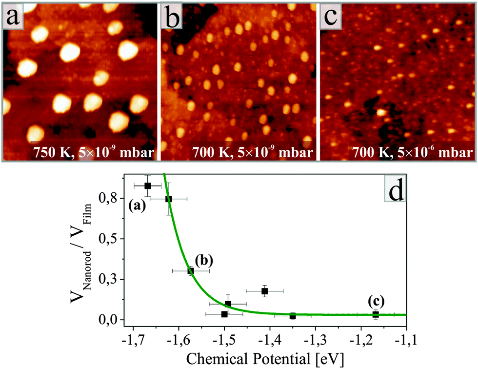 | ||
| Fig. 3 (a–c) ZnO films prepared at different temperatures and O2 pressures as indicated in the panels. Note the varying density and size of the ZnO nanorods. (Us = 2.4 V, 100 × 100 nm2). (d) Ratio between nanorod volume and total amount of deposited material, plotted as a function of the oxygen chemical potential. An exponential relationship has been fitted as guide to the eye. | ||
Before rationalizing the observed behaviour, we will prove that the nanorods are indeed made of ZnO and do not contain un-reacted Zn metal or gold segregated from the support. For this purpose, we have acquired STM conductance spectra on top of the nanorods and the flat film via lock-in techniques (Fig. 4a). In both cases, the curves clearly reveal the oxide band gap, characterized by a broad zero-conductance region around the Fermi level. The conduction-band edge is consistently found at +0.5 V, while the onset of the valence band varies between −1.5 and −2.5 V. This variation depends on the setpoint value for spectroscopy rather than the actual tip position above a nanorod or the flat film. Typically, a more negative band-onset is revealed for a larger setpoint bias (increased tip–sample separation), while the conductivity onset shifts towards the Fermi level in low-bias spectra. This trend suggests that the observed variability is caused by band-bending effects due to the tip-electric field and provides no indication on the metallicity of the rods. In all cases, the vanishing conductance around the Fermi level safely points to a semi-conducting, ZnO-type character of the different nanostructures.
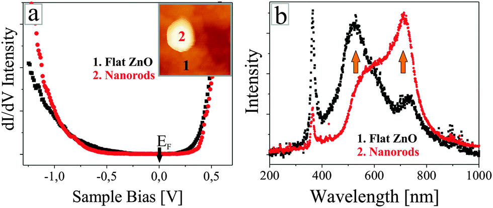 | ||
| Fig. 4 (a) STM conductance spectra taken on a single ZnO nanorod and the surrounding flat film. Evidently, both materials have the same chemical identity. (b) STM luminescence spectra of flat ZnO films and films covered with nanorods. Note the different intensities of the 535 and the 730 nm defect peak that are assigned to Zn and O vacancies, respectively. | ||
The O2 chemical potential adjusted in the last annealing step also governs the optical properties of the oxide. Fig. 4b shows two STM luminescence spectra taken either on a homogenous ZnO film (black curve) or a nanorod sample (red curve). The measurements were performed by injecting 150 eV electrons (5 nA current) from the STM tip into a preselected oxide region and accumulating the emitted photons for 300 s with the CCD detector. The two spectra display a sharp luminescence peak at 373 nm, readily assigned to the band–band recombination in wurtzite ZnO. In addition, two defect peaks are resolved at 535 and 730 nm, being related to Zn and O vacancies, respectively, as discussed in earlier work.26,27 The intensity difference of the defect peaks is in line with the specific preparation conditions of the ZnO samples. Upon oxygen-rich annealing, the O-vacancy peak is considerably weaker than the emission from Zn vacancies, indicating that Zn defects occur predominately in the oxide lattice. Conversely, film preparation at low O2 chemical potential results in a strong O-defect peak at 730 nm, while Zn vacancies only produce a faint shoulder at 535 nm. The intensity ratio of O to Zn vacancy peaks thus provides direct insight into the oxide stoichiometry, proving that nanorod samples are indeed oxygen poor. We note that Zn defects cannot fully be eliminated even at very low O2 chemical potential, as this defect type ensures the charge neutrality in n-type, hence electron rich ZnO.
Based on these experimental results, we now discuss possible reasons for the impact of the O2 chemical potential on the ZnO morphology. In general, we find a preferential growth of oxide nanorods at low chemical potentials, while flat and homogenous films are formed at oxygen-rich conditions and moderate temperatures. The following scenario aims to explain this behaviour. In our first preparation step, room-temperature deposition of ZnO, a likely amorphous precursor film develops on the Au(111) support, which does not exhibit any LEED pattern. Only upon annealing in the second step, the Zn and O ions gain sufficient mobility to develop a long-range crystallographic order. Also, the one-to-one stoichiometry of the oxide gets established at this point, a process that involves desorption of excess Zn and dissociation of additional gas-phase O2 to balance the oxygen loss during heating. Especially, the latter process appears to be crucial for the final film morphology. At high O2 chemical potential, enough oxygen is available to saturate all Zn cations and to produce a stoichiometric film exposing the preferred {0001} termination.28 The weak O-defect peak with respect to Zn-vacancies in luminescence spectra confirms the oxygen surplus in these samples (Fig. 4b). The situation changes at low O2 chemical potential, when the oxygen supply becomes the bottleneck for oxide growth. The lack of oxygen is responsible for enhanced Zn desorption, followed by a thinning of the film with respect to O2-rich conditions. Moreover, the film contains an abundance of O vacancies, as deduced from the optical spectra.26
Interestingly, the oxygen supply seems sufficient in certain regions of the surface, leading to the formation of ZnO nanorods. We propose that traces of Au from the support help catalysing the oxide growth at these sites. The Au(111) surface features an exceptionally large room-temperature fluxionality due to its dense and highly mobile lattice gas.29 The diffusing adatoms were found to be responsible for various surface science phenomena, e.g. the formation of self-assembled thiolate monolayers,30 gold nanofingers,31 or metal–organic complexes.32 Given their high mobility at 300 K, we propose that a part of the adatoms remain on the surface during film deposition, while the majority gets buried at the metal–oxide interface. The surface Au species now become active in catalysing further ZnO growth in the final annealing step. Following the vapour–liquid–solid (VLS) mechanism,1,12 a local alloying of Au and Zn hereby produces an highly active phase for O2 dissociation, overcoming the lack of oxygen at low O2 chemical potentials. We emphasize that the presence of tiny Au quantities plays no role in oxygen excess, when the ZnO growth is not limited by the oxygen supply. At this condition, the oxide film exhibits a layer by layer growth and nanorod formation is of minor importance.
Indirect evidence for our growth model comes from high-resolution STM images of individual ZnO nanorods, as shown in Fig. 5. On sufficiently large rods, we have detected a regular line pattern that occurs in three domains rotated by 120°. The periodicity of the pattern amounts to 5.5 Å, being twice the spacing of the close-packed O or Zn rows on the {0001} surface. We ascribe this pattern to Au rows that decorate the top facet of the nanorod and might have been involved in catalysing its growth (Fig. 5c). Note that only a disordered adsorbate phase, but no regular stripe pattern was found on the flat oxide films (Fig. 5a).
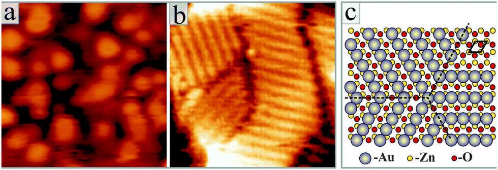 | ||
| Fig. 5 High-resolution STM images taken on (a) a flat ZnO film and (b) a nanorod top-facet (Us = 3 V, 6.5 × 6.5 nm2). While the flat film exposes a disordered adsorbate phase, made of hydroxyl groups, the nanorod surface shows a characteristic line pattern in three rotational domains. The lines are made of Au atoms, as depicted in the ball model shown in (c). | ||
The Au termination of the nanorods fulfils another task. The {0001} surfaces of ZnO are polar and the associated dipole moment needs to be cancelled in order to stabilize the 3D islands.33 Mathematically, dipole compensation is achieved by generating a surface charge-density σsurf that depends on the bulk charge-density via the universal compensation rule: 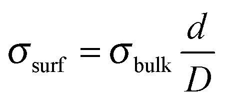 .34 Here, d and D are the Zn–O layer distance (0.63 Å) and the unit cell height of the wurtzite lattice (2.56 Å), respectively. The critical surface charge-density of ±0.5 |e| might be generated by placing a singly-charged Au ion on every second unit cell, hence producing a 2 × 1 superstructure, as depicted in Fig. 5b. The actual charge state of the adatoms hereby depends on the stacking sequence of the nanorods. While Au+ ions would compensate for the polarity of an O-terminated surface, Au− species should be placed on the Zn-terminated oxide plane. Given the high electronegativity of gold, we consider the latter scenario more likely. Note that flat ZnO films were found to be O-terminated24 and their polarity gets cancelled via a disordered hydrogen ad-layer (Fig. 5a).35 We can discard this possibility for the top-facets of ZnO rods, which exhibit a corrugation of 2.5 Å, much larger than the one of the hydrogen termination. The large surface corrugation of the nanorods and their mere existence therefore support the idea of an Au-catalysed growth of ZnO on an Au(111) surface.
4. Conclusions
We have demonstrated that small changes in the O2 chemical potential drastically affect the growth of ZnO on an Au(111) support. While a layer by layer growth is observed at oxygen-rich conditions, resulting in flat (000)-terminated ZnO films, formation of nanorods with large aspect ratio is revealed in an O2 poor environment. We ascribe this phenomenon to the critical role of the oxygen supply in the high-temperature crystallization step of the oxide. Homogenous films develop only in oxygen excess, while traces of surface gold that help trapping and dissociating the O2 molecules promote the nanorod growth at oxygen-poor conditions. Indirect evidence for this scenario comes from a distinct line pattern observed on top of the ZnO rods that is compatible with an Au(2 × 1) ad-layer. In order to confirm the proposed mechanism, the accumulation of gold on the oxide surface needs to be verified either by ion scattering or photoelectron spectroscopy in future.
The growth of ZnO nanorods by physical-vapour deposition in a vacuum environment represents an interesting pathway to fabricate pure nanostructures for optical and catalytic applications. The choice of Au(111) as support material turns out to be particularly suited in this respect, given its high activity in the VLS regime. However, other metal substrates are expected to promote the formation of ZnO nanostructures in a similar way.
Acknowledgements
The authors acknowledge support from the DFG Cluster of Excellence ‘UniCat’ and the COST Action CM1104 ‘Reducible oxides’. F. S. and L. P. thank the ‘Alexander von Humboldt Stiftung’ and the Max Planck Research School ‘Functional Interfaces in Physics and Chemistry’ for financial support.References
- Ü. Özgür, Ya. I. Alivov, C. Liu, A. Teke, M. A. Reshchikov, S. Doğan, V. Avrutin, S.-J. Cho and H. Morkoç, J. Appl. Phys., 2005, 98, 041301 CrossRef PubMed.
- C. Wöll, Prog. Surf. Sci., 2007, 82, 55–120 CrossRef PubMed.
- Z. L. Wang, J. Phys.: Condens. Matter, 2004, 16, R829–R858 CrossRef CAS.
- C. Tusche, H. L. Meyerheim and J. Kirschner, Phys. Rev. Lett., 2007, 99, 026102 CrossRef CAS.
- Z. R. Dai, Z. W. Pan and Z. L. Wang, Adv. Funct. Mater., 2013, 13, 9–24 CrossRef.
- D. F. Liu, Y. J. Xiang, Q. Liao, J. P. Zhang, X. C. Wu, Z. X. Zhang, L. F. Liu, W. J. Ma, J. Shen, W. Y. Zhou and S. S. Xie, Nanotechnology, 2007, 18, 405303 CrossRef.
- Q. F. Zhang, C. S. Dandeneau, X. Y. Zhou and G. Z. Cao, Adv. Mater., 2009, 21, 4087–4108 CrossRef CAS.
- J. Agrell, H. Birgersson, M. Boutonnet, I. Melian-Cabrera, R. M. Navarro and J. L. G. Fierro, J. Catal., 2003, 219, 389–403 CrossRef CAS.
- J. Y. Park, Y. S. Yun, Y. S. Hong, H. Oh, J. J. Kim and S. S. Kim, Appl. Phys. Lett., 2005, 87, 123108 CrossRef PubMed.
- Y. Zhang, H. B. Jia, R. M. Wang, C. P. Chen, X. H. Luo, D. P. Yu and C. J. Lee, Appl. Phys. Lett., 2003, 83, 4631 CrossRef CAS PubMed.
- L. E. Greene, M. Law, D. H. Tan, M. Montano, J. Goldberger, G. Somorjai and P. D. Yang, Nano Lett., 2005, 5, 1231–1236 CrossRef CAS.
- X. D. Wang, C. J. Summers and Z. L. Wang, Nano Lett., 2004, 4, 423–426 CrossRef CAS.
- D. Ito, M. L. Jespersen and J. E. Hutchison, ACS Nano, 2008, 2, 2001–2006 CrossRef CAS PubMed.
- Z. W. Pan, Z. R. Dai and Z. L. Wang, Science, 2001, 291, 1947–1949 CrossRef CAS PubMed.
- Z. L. Wang, J. Phys.: Condens. Matter, 2004, 16, R829–R858 CrossRef CAS.
- X. Duan, Y. Huang, Y. Cui, J. Wang and C. M. Lieber, Nature, 2001, 409, 66–69 CrossRef CAS PubMed.
- E. V. Batyrev, et al. , Phys. Chem. Chem. Phys., 2011, 13, 13127–13134 RSC.
- F. Ostendorf, S. Torbrügge and M. Reichling, Phys. Rev. B: Condens. Matter Mater. Phys., 2008, 77, 041405(R) CrossRef.
- B. Meyer, D. Marx, O. Dulub, U. Diebold, M. Kunat, D. Langenberg and C. Wöll, Angew. Chem., Int. Ed., 2004, 43, 6641 CrossRef CAS PubMed.
- O. Dulub, U. Diebold and G. Kresse, Phys. Rev. Lett., 2003, 90, 016102 CrossRef.
- G. Weirum, G. Barcaro, A. Fortunelli, F. Weber, R. Schennach, S. Surnev and F. P. Netzer, J. Phys. Chem. C, 2010, 114, 15432–15439 CAS.
- F. Stavale, L. Pascua, N. Nilius and H.-J. Freund, J. Phys. Chem. C, 2013, 117, 10552–10557 CAS.
- M. H. Huang, S. Mao, H. Feick, H. Yan, Y. Wu, H. Kind, E. Weber, R. Russo and P. Yang, Science, 2001, 292, 1897–1899 CrossRef CAS PubMed.
- H.-J. Freund, N. Nilius, T. Risse, S. Schauermann and T. Schmidt, ChemPhysChem, 2011, 12, 79 CrossRef CAS PubMed.
- P. Atkins and J. De Paula, Physical Chemistry, University Press, Oxford, 2006 Search PubMed.
- F. Stavale, N. Nilius and H.-J. Freund, J. Phys. Chem. Lett., 2013, 4, 3972–3976 CrossRef CAS.
- A. Janotti and C. G. Van de Walle, Phys. Rev. B: Condens. Matter Mater. Phys., 2007, 76, 165202 CrossRef.
- Due to the high electronegativity of the Au(111) support, our films are oxygen terminated and covered with a (000) surface.
- G. E. Poirier and E. D. Pylant, Science, 1996, 272, 1145–1148 CAS.
- M. Yu, N. Bovet, C. J. Satterley, S. Bengio, K. R. J. Lovelock, P. K. Milligan, R. G. Jones, D. P. Woodruff and V. Dhanak, Phys. Rev. Lett., 2006, 97, 166102 CrossRef.
- F. Yin, R. E. Palmer and Q. Guo, J. Phys.: Condens. Matter, 2009, 21, 445001 CrossRef CAS PubMed.
- B. Yang, X. Lin, Y. Pan, N. Nilius, H.-J. Freund, C. Hulot, A. Giraud, S. Blechert, S. Tosoni and J. Sauer, J. Am. Chem. Soc., 2012, 134, 11161–11167 CrossRef CAS PubMed.
- V. Staemmler, K. Fink, B. Meyer, D. Marx, M. Kunat, S. G. Girol, U. Burghaus and C. Wöll, Phys. Rev. Lett., 2003, 90, 106102 CrossRef CAS.
- J. Goniakowski, F. Finocchi and C. Noguera, Rep. Prog. Phys., 2008, 71, 016501 CrossRef.
- J. V. Lauritsen, S. Porsgaard, M. K. Rasmussen, M. C. Jensen, R. Bechstein, K. Meinander, B. S. Clausen, S. Helveg, R. Wahl, G. Kresse and F. Besenbacher, ACS Nano, 2011, 5, 5987–5994 CrossRef CAS PubMed.
| This journal is © the Owner Societies 2014 |