 Open Access Article
Efficient organic–inorganic hybrid perovskite solar cells processed in air
Madhu
Seetharaman S
a,
Puvvala
Nagarjuna
b,
P. Naresh
Kumar
c,
Surya Prakash
Singh
b,
Melepurath
Deepa
c and
Manoj A. G.
Namboothiry
*a
aSchool of Physics, Indian Institute of Science Education & Research, Computer Science Building, College of Engineering Trivandrum Campus, Trivandrum-695016, Kerala, India. E-mail: manoj@iisertvm.ac.in
bInorganic and Physical Chemistry Division, CSIR-Indian Institute of Chemical Technology, Ministry of Science & Technology, Government of India, Tarnaka, Hyderabad-500007, Telangana, India
cDepartment of Chemistry, Indian Institute of Technology Hyderabad, Ordnance Factory Estate, Yeddumailaram-502205, Telangana, India
First published on 24th September 2014
Abstract
Organic–inorganic hybrid perovskite solar cells with fluorine doped tin oxide/titanium dioxide/CH3NH3PbI3−xClx/poly(3-hexylthiophene)/silver were made in air with more than 50% humidity. The best devices showed an open circuit voltage of 640 mV, a short circuit current density of 18.85 mA cm−2, a fill factor of 0.407 and a power conversion efficiency of 5.67%. The devices showed external quantum efficiency varying from 60 to 80% over a wavelength region of 350 nm to 750 nm of the solar spectrum. The morphology of the perovskite was investigated using scanning electron microscopy and it was found to be porous in nature. This study provides insights into air-stability of perovskite solar cells.
Introduction
Organic–inorganic hybrid perovskite materials are of great interest for optoelectronic applications. Recently, light emitting diodes and field effect transistors based on perovskites have been reported, where the perovskites were synthesized by mixing methyl ammonium iodide (CH3NH3I) and lead iodide in organic solvents followed by annealing.1,2 This was followed by reports on photovoltaic properties of the same material in dye sensitized solar cells.3–6 Perovskite materials based on methyl ammonium iodide mixed with lead iodide are widely used as active materials in perovskite solar cells as they can be solution processed and are cost effective. Over the last few years, this material and its derivatives have delivered power conversion efficiency (PCE) exceeding 19%,7 which generated a lot of interest in the solid state dye sensitised photovoltaic research community.Even though CH3NH3PbI3 based cells have shown promise with very high PCEs, they are found to be unstable and tend to undergo fast degradation in performance in the presence of an electrolyte.3,8 It is reported that the hygroscopic properties of the methyl ammonium cation make it difficult to process solar cells under ambient air conditions using this material, without the use of an inert atmosphere. Additionally, these cells require a nanostructured or a mesoporous layer of TiO2 for electron extraction resulting in a high performance.5,8–10 A new mixed halide perovskite material, CH3NH3PbI3−xClx, used an Al2O3 scaffold instead of a mesoporous TiO2 layer, which showed high performances with a boost in open circuit voltage resulting in a PCE of above 10%.9,11–14
The mixed halide CH3NH3Pb3−xClx perovskite was found to be more stable and at the same time has better carrier transport properties than the CH3NH3PbI3 perovskite material.15 Furthermore, the CH3NH3Pb3−xClx perovskite was found to exhibit ambipolar transport behaviour, which aided in developing simple planar structured cells, with an extremely thin absorber (ETA) layer. Simultaneously, a solid state hole transporting (HTM) material, Spiro-MeOTAD (2,2′,7,7′-tetrakis(N,N-di-p-methoxyphenylamine)-9,9′-spirobifluorene), was used in these cells as it can penetrate through the porous perovskite layer and provide a better contact for charge transportation.3,9,16,17 Other alternatives and less costly organic HTM materials like poly tri-aryl amine (PTAA), poly(3-hexylthiophene-2,5-diyl) (P3HT) and inorganic materials such as Copper iodide (CuI) have also been used in the past18–25 and high performance devices were achieved. One of the challenges in making solution processed devices is their fast degradation in the presence of moisture in the atmosphere.
In this article, an organic–inorganic mixed halide perovskite solar cell with CH3NH3PbI3−xClx as an extremely thin absorber material and P3HT as a HTM over a thin film layer of dense TiO2 as an electron transport material (ETM) is reported. The devices were made under ambient air conditions with humidity greater than 50%. Most of the reported high efficiency solution processed perovskite based photovoltaic devices were fabricated under controlled atmospheric conditions with water and oxygen content less than 1 ppm levels. An undoped P3HT was used as a hole transporting layer as our recent modelling studies have revealed that such an undoped hole transporting layer can enhance the photovoltaic properties of perovskite solar cells.
Experimental methods
Device fabrication
Fluorine-doped tin oxide (FTO) glasses (Pilkington) were cleaned by ultrasonication with ethanol for 30 minutes and treated in a UV Ozone cleaner for 30 min. The cleaned FTO glasses were coated with 0.15 M titanium diisopropoxide bis(acetylacetonate) (75% by wt in isopropanol, Aldrich) in 1-butanol (Aldrich) solution by the spin-coating method at 2000 rpm for 60 s, followed by heating at 125 °C. The films were cooled down to room temperature and a 0.3 M titanium diisopropoxide bis(acetylacetonate) solution in 1-butanol was spin coated. The procedure was repeated twice to make a pin hole free dense TiO2 film.8 The substrates were annealed in a box furnace at 450 °C for 60 minutes. The perovskite sensitizer CH3NH3I was prepared according to the reported procedure.26 A mixture of hydroiodic acid (57 wt% in water, Aldrich) and methylamine (40% in methanol, Aldrich) was stirred in an ice bath for 2 hours. After stirring at 0 °C for 2 hours, the resulting solution was evaporated at 50 °C for 1 hour and methyl ammonium iodide was obtained. The precipitate was washed three times with diethyl ether and dried in a vacuum under dark conditions.For preparing the CH3NH3PbI3−xClx layer, methylammonium iodide (CH3NH3I) and lead(II) chloride (PbCl2, Aldrich) were dissolved in anhydrous N,N-dimethyl formamide (DMF, Aldrich) mixed in a 3![[thin space (1/6-em)]](https://www.rsc.org/images/entities/char_2009.gif) :
:![[thin space (1/6-em)]](https://www.rsc.org/images/entities/char_2009.gif) 1 molar ratio of CH3NH3I to PbCl2, to make the 30% and 40% by weight precursor solutions. The 40 wt% and 30 wt% solutions were spin coated at 2000 rpm and 1500 rpm, respectively, for 45 s to make perovskite films of uniform thickness for device performance comparison. The substrates were subsequently heated at 100 °C on a hot plate, under dark conditions, for 90 minutes.27 The hole transporting layer of poly(3-hexylthiophene-2,5-diyl) (P3HT) was prepared by spin coating a 15 mg mL−1 solution in chlorobenzene at 1500 rpm for 2 min. The substrates were loaded into a vacuum thermal evaporator and a 120 nm thick layer of silver (Ag) was thermally evaporated to act as the counter electrode at a pressure of 6 × 10⁻⁶ mbar. A number of devices were made for making a statistical comparison. The thickness of each layer was measured using a Dektak 6M stylus profilometer. The thickness of each layer of the optimized device with a correction factor of ±5 nm is as follows: TiO2 blocking layer ∼ 120 nm, perovskite layer ∼ 250 nm, P3HT layer ∼ 100 nm and Ag layer ∼ 120 nm. The active area of the device is 0.09 cm2.
1 molar ratio of CH3NH3I to PbCl2, to make the 30% and 40% by weight precursor solutions. The 40 wt% and 30 wt% solutions were spin coated at 2000 rpm and 1500 rpm, respectively, for 45 s to make perovskite films of uniform thickness for device performance comparison. The substrates were subsequently heated at 100 °C on a hot plate, under dark conditions, for 90 minutes.27 The hole transporting layer of poly(3-hexylthiophene-2,5-diyl) (P3HT) was prepared by spin coating a 15 mg mL−1 solution in chlorobenzene at 1500 rpm for 2 min. The substrates were loaded into a vacuum thermal evaporator and a 120 nm thick layer of silver (Ag) was thermally evaporated to act as the counter electrode at a pressure of 6 × 10⁻⁶ mbar. A number of devices were made for making a statistical comparison. The thickness of each layer was measured using a Dektak 6M stylus profilometer. The thickness of each layer of the optimized device with a correction factor of ±5 nm is as follows: TiO2 blocking layer ∼ 120 nm, perovskite layer ∼ 250 nm, P3HT layer ∼ 100 nm and Ag layer ∼ 120 nm. The active area of the device is 0.09 cm2.
Measurements and characterization
The X-ray diffraction pattern of the perovskite was measured on an X-Pert Pro Analytical diffractometer. Morphology and microstructural characterization were performed using a field emission scanning electron microscope (Nova NanoSEM NPE 206 high resolution SEM). The coverage of the perovskite was calculated by processing the scanning electron microscope image of the film using the grayscale threshold method in open source software, ImageJ.28 UV-Vis absorption spectra were acquired using a SHIMADZU UV-3600 spectrophotometer. The current–voltage characteristics of the devices were measured using a Keithley 6430 source meter in the dark and under an illumination of the 1000 W m−2 AM1.5G spectrum using an Oriel 3A solar simulator tested using a NREL calibrated silicon solar cell. The external quantum efficiency (EQE) measurements were done using a lock-in technique with a 250 W xenon lamp coupled with a Newport monochromator and chopped at 40 Hz with a light chopper blade as the light source. A lock-in amplifier (SRS 830, Stanford Research Systems Inc., USA) was used to measure currents and a NIST calibrated silicone photodiode was used to find the incident power spectral response of the incident light. The measurements were done using shadow masks to avoid edge effects and an appropriate mismatch factor was taken to square off the spectral mismatch for calculating PCE and EQE.29,30Results and discussion
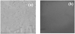
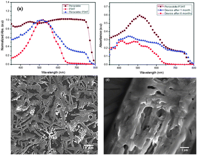
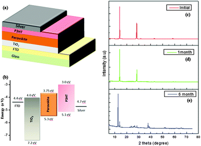
The mixed halide perovskite was spin coated under ambient conditions, on a plane glass plate and was observed. The film was transparent before annealing and turned to dark brown upon annealing as shown in Fig. 1. Unlike CH3NH3PbI3, the mixed halide perovskite remained in the same state without any change for more than one month when coated with a layer of P3HT and is confirmed using the UV-Vis studies of CH3NH3PbI3−xClx/P3HT bilayer structures. The UV-Vis absorbance spectrum of the CH3NH3PbI3−xClx/P3HT bilayer, single layers of CH3NH3PbI3−xClx and P3HT of similar thickness as used in optimized device structure is shown in Fig. 2(a). The absorption spectrum of the CH3NH3PbI3−xClx/P3HT bilayer of film thickness similar to that of the actual device shows features of both P3HT and perovskite. P3HT has an absorption edge at a wavelength (λ) of ∼640 nm with a shoulder at λ ∼ 600 nm and a peak at λ ∼ 520 nm. The perovskite showed a broad absorption peak with an edge at λ ∼ 800 nm and a peak at λ ∼ 450 nm. Even though a perovskite layer of thickness 250 nm should absorb all the light incident on it due to an absorption coefficient of ∼105 cm−1,31 poor coverage of perovskite films makes light to pass through them and results in absorption contribution from P3HT in the bilayer structure. The SEM images (Fig. 2(c) and (d)) of the mixed halide perovskite show the porous nature of the CH3NH3PbI3−xClx film validating the reason for P3HT contribution in the UV-Vis spectrum of the bilayer structure. The needle structure of the perovskite as seen from the SEM image can be attributed to the increased absorbance of the perovskite film in the longer wavelength region due to increased internal scattering in such kinds of structures.25The absorption data of the perovskite/P3HT bilayer coated on a plane glass plate of similar thickness to that in the actual device (made at the time of device fabrication) are compared with absorption spectra of actual device FTO/TiO2/perovskite/P3HT/Ag (absorption spectra were recorded on the device where Ag was not coated) after one month and of that after 6 months as shown in Fig. 2(b) to study the stability of the perovskite layer. The absorption spectra of the bilayer after one month show a change in the spectral envelope in the spectral region attributed to the contribution from P3HT (450 nm < λ < 600 nm) showing degradation of P3HT over time. The spectral envelope remains unchanged in the spectral window, which is attributed to the perovskite (650 nm < λ < 800 nm and λ < 450 nm) and can be attributed to a stable perovskite layer. Further storage of the device under ambient conditions over a period of 6 months showed degradation of the perovskite layer and is attributed to the disappearance of the spectral features in the λ region from 650 nm to 800 nm. The X-ray diffraction analysis of the mixed halide perovskite shows characteristic peaks at 14.1° and 28.5° (Fig. 3(c)). The X-ray analysis of the perovskite films even after one month (Fig. 3(d)) showed the same peaks with unaltered peak positions, thus illustrating that there is no significant degradation of the perovskite film with time. However, the films after 6 months show a change in the peak position (Fig. 3(e)), with a prominent peak at 12.7°, indicating the presence of PbI2, due to the degradation of the perovskite.27 The film retained the same morphology without any change, when stored for a period of more than a month. After confirming the stability of the perovskite by different methods, photovoltaic devices were made with the device structure, FTO/TiO2/CH3NH3PbI3−xClx/P3HT/Ag. A schematic of the device structure and the energy level diagram of different materials used in the device are shown in Fig. 3(a) and (b) respectively.
A TiO2 dense layer with a thickness of about 120 nm was used as an electron transporting, hole blocking layer. It has been reported earlier that the mixed perovskite diffusion lengths for electrons and holes are typically, in the order of 1 micron, with a good ambipolar behaviour.15 The optimal thickness of the perovskite was 250 nm. Our recent dark I–V modelling study revealed that an undoped hole transporting layer is better for reducing the space charge effects.32 Hence, one of the commonly used p-type polymers, P3HT, was employed herein, as the hole transporting layer in the devices. The P3HT film thickness was optimized at 100 nm for highest efficiency devices. All these layers were solution processed in air; they were spin coated under ambient conditions with humidity levels in excess of 50%. One of the main factors affecting the performance of the perovskite solar cell is the thickness and the film quality of the active layer. The formation of pin-holes can cause the hole transport material and electron transport material to come in contact, resulting in the formation of parallel paths, causing high shunt resistance and recombination of electrons and holes. Even though better coverage is achieved over TiO2 by increasing the thickness of the TiO2 layer and the concentration of the perovskite precursor solution, the maximum coverage of the perovskite film is around 95% of the surface area only in the literature.12,26 The SEM images of the perovskite active layer show decent coverage over the dense TiO2 layer and about 75% coverage at higher magnification with needle like structures Fig. 2(c). The film was found to be porous in nature at higher magnification (Fig. 2(d)).
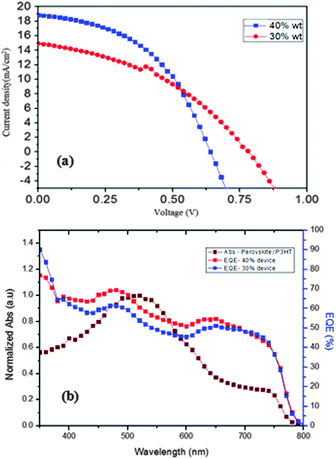
The devices were made using different concentrations of CH3NH3PbI3−xClx. The dark current characteristics show a diode like behaviour. The J–V (current density vs. voltage) characteristics were recorded under A.M.1.5G, 1 Sun illumination (Fig. 4(a)). The devices with 30% (by wt) solution of the perovskite precursor gave a PCE of 4.79% with a short circuit current density (Jsc) of 14.98 mA cm−2, an open circuit voltage (Voc) of 781 mV and a fill factor (FF) of 0.409. In order to enhance the solar cell performance, the concentration of the perovskite solution was increased to 40% (by wt). When the process was repeated using 40% (by wt) solution of the perovskite precursor, the PCE was observed to increase to 5.67% with a Jsc of 18.85 mA cm−2, a Voc of 640 mV and an FF of 0.407. Jsc was found to increase when the concentration of the solution was increased, Voc was found to decrease and FF was found to be almost similar. The increase in Jsc is attributed to the improvement in the absorption of the perovskite layer made of 40 wt% solutions due to its better surface coverage. The perovskite films prepared from 40 wt% solution have a surface coverage of 75% and those made from 30 wt% solutions have a surface coverage of 63%. The Voc decrease can be attributed to the intercalation of different layers into each other due to the porous nature of the active layer.
The PCE values are comparable to the values in the literature obtained for solution processed perovskite solar cells that are made in a controlled atmosphere. The EQE spectra (Fig. 4(b)) showed the incident photon to current conversion efficiency varying from 60 to 80% over a wavelength region of 350 to 750 nm of the solar spectrum with an edge extending to the near-infrared region at a wavelength of 800 nm. Comparison of EQE of the device and absorption spectra of the CH3NH3PbI3−xClx/P3HT bilayer shows that the EQE of the device is resultant of photocurrent generation in P3HT and the perovskite and the effective transport of free carriers to the electrode through these layers. It is to be noted that P3HT shows an excitonic feature resulting in the formation of excitons (bound electron hole pair) as the primary photoexcited species. But in the perovskite, due to its high dielectric constant,33 free electrons and holes are created upon photoexcitation. In the λ region ranging from 800 nm to 650 nm the photocurrent observed is due to the perovskite. The electrons and holes which are formed in the perovskite, especially near the CH3NH3PbI3−xClx/P3HT interface, are well transferred to the electrodes through the perovskite and hole transporting P3HT. There is a significant light harvesting in this λ region with a reduced ratio of EQE ratio numbers of peaks at λ ∼ 520 nm to that at 750 nm compared to the ratio of absorbance of the bilayer at these respective λs, This can be attributed to good electronic transport of the perovskite. The peak at λ ∼ 640 nm can be due to the increased absorption of the bilayer with P3HT contributing to the photocurrent by producing free charge carriers due to dissociation of excitons created in P3HT (at the absorption edge of P3HT) at the P3HT/perovskite interface. EQE for λ < 640 nm is a net result of photocarriers created in the perovskite and P3HT and its effective transport across the device. Deviation of EQE spectra from absorption spectra for λ < 620 nm can be attributed to reduced contribution from P3HT due to the creation of charge transfer excitons in P3HT. High energy photons are needed to dissociate this charge transfer excitons and this results in a EQE peak at λ ∼ 485 nm, which is blue shifted compared to the bilayer absorption peak. In the shorter wavelength region perovskite absorption prevails and it follows the absorption spectra. The observed increase in EQE of solar cells (in the λ range of 400 nm to 650 nm) made using 40 wt% solution compared to that of 30 wt% solution can be due to increased absorption of the perovskite layer made using 40 wt% solution. Most of the light in this spectral region has a penetration depth which is less than the thickness of the perovskite film due to an absorption coefficient of 105 cm−1. It has been observed that the poor coverage of the perovskite film reduces light absorption in this spectral region. Hence the enhancement of EQE in this spectral region is due to the better coverage of perovskite films made from 40 wt% solution compared to that made from 30 wt% solutions. A histogram of PCE values of 50 different cells obtained in our lab is given for consistency and reproducibility in Fig. 5.
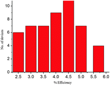 | ||
| Fig. 5 Histogram of the number of devices with the corresponding power conversion efficiencies obtained. | ||
The devices were stored in an air tight container and characterized after 50 days. The PCE dropped drastically to 0.11% with a Jsc of 1.05 mA cm−2, a Voc of 323 mV and an FF of 0.32. This shows the degradation of the device under humid air conditions. Furthermore, reduction in the performance of the device can be attributed to the silver electrodes which were found to have deteriorated with time, in accordance with the observation by Snaith et al.34 and due to degradation of P3HT over time as seen from the UV-Vis spectrum studies. The halide ion in the perovskite can result in the degradation of the silver electrode to silver halides, thus adversely impacting the performance of the device. Various other top electrodes such as gold and aluminium were used to replace Ag, but they resulted in poor device performance with a PCE of less than 2%. It can be concluded that cell degradation is mainly caused by the oxidation of the silver electrode and P3HT, over a period of time.
Conclusions
A solid state dye sensitized solar cell based on an organic–inorganic hybrid perovskite using CH3NH3Pb3−xClx is made with high performance and efficiency under highly humid and ambient air conditions by a spin coating method. Best performing FTO/TiO2/CH3NH3Pb3−xClx/P3HT/Ag solar cells processed with 40 wt% perovskite solutions showed a PCE of 5.67% with a Jsc of 18.85 mA cm−2, a Voc of 640 mV and a FF of 0.407. The EQE showed contribution from both P3HT and perovskite, with P3HT collecting the unabsorbed light through the perovskite due to its poor coverage. The XRD and UV-Vis studies showed that the perovskite layer is stable for a period of one month. The observed degradation is attributed to a collective effect of P3HT degradation as observed in the UV-Vis studies and that due to Ag oxidation. Future studies are pursued to enhance the perovskite surface coverage as it is sensitive to the concentration of perovskite solution used for spin coating and annealing temperature.Acknowledgements
The authors thank the Department of Science and Technology (DST/TM/SERI/2k11/73(G)) Solar Energy Research Initiative project, Ministry of Human Resource Development and Govt. of India, and the Amorphous Silicon Solar Cell Plant, Bharat Heavy Electricals Limited, Gurgaon, India.Notes and references
- J. H. Im, C. R. Lee, J. W. Lee, S. W. Park and N. G. Park, Nanoscale, 2011, 3, 4088–4093 RSC.
- T. Baikie, Y. Fang, J. M. Kadro, M. Schreyer, F. Wei, S. G. Mhaisalkar, M. Graetzel and T. J. White, J. Mater. Chem. A, 2013, 1, 5628 CAS.
- M. He, D. Zheng, M. Wang, C. Lin and Z. Lin, J. Mater. Chem. A, 2014, 2, 5994–6003 CAS.
- J. Burschka, N. Pellet, S. J. Moon, R. H. Baker, P. Gao, M. K. Nazeeruddin and M. Gratzel, Nature, 2013, 499, 316–319 CrossRef CAS PubMed.
- A. Kojima, K. Teshima, Y. Shirai and T. Miyasaka, J. Am. Chem. Soc., 2009, 131, 6050–6051 CrossRef CAS PubMed.
- H. S. Kim, J. W. Lee, N. Yantara, P. P. Boix, S. A. Kulkarni, S. Mhaisalkar, M. Grätzel and N. G. Park, Nano Lett., 2013, 13, 2412–2417 CrossRef CAS PubMed.
- H. Zhou, Q. C. G. Li, S. Luo, T. Song, H. S Duan, Z. Hong, J. You, Y. Liu and Y. Yang, Science, 2014, 345, 542–546 CrossRef CAS PubMed.
- S. Kim, C.-R. Lee, J. H. Im, K. B. Lee, T. Moehl, A. Marchioro, S. J. Moon, R. H. Baker, J. H. Yum, J. E. Moser, M. Gratzel and N. G. Park, Sci. Rep., 2012, 2, 591 Search PubMed.
- M. M. Lee, J. Teuscher, T. Miyasaka, T. N. Murakami and H. J. Snaith, Science, 2012, 338, 643–647 CrossRef CAS PubMed.
- V. G. Pedro, E. J. J. Perez, W. S. Arsyad, E. M. Barea, F. F. Santiago, I. M. Sero and J. Bisquert, Nano Lett., 2014, 14, 888–893 CrossRef PubMed.
- M. J. Carnie, C. Charbonneau, M. L. Davies, J. Troughton, T. M. Watson, K. Wojciechowski, H. Snaith and D. A. Worsley, Chem. Commun., 2013, 49, 7893–7895 RSC.
- M. Liu, M. B. Johnston and H. J. Snaith, Nature, 2013, 501, 395–398 CrossRef CAS PubMed.
- S. Colella, E. Mosconi, P. Fedeli, A. Listorti, F. Gazza, F. Orlandi, P. Ferro, T. Besagni, A. Rizzo, G. Calestani, G. Gigli, F. De Angelis and R. Mosca, Chem. Mater., 2013, 25, 4613–4618 CrossRef CAS.
- G. Niu, W. Li, F. Meng, L. Wang, H. Dong and Y. Qiu, J. Mater. Chem. A, 2014, 2, 705–710 CAS.
- S. D. Stranks, G. E. Eperon, G. Grancini, C. Menelaou, M. J. P. Alcocer, T. Leijtens, L. M. Herz, A. Petrozza and H. J. Snaith, Science, 2012, 342, 341–344 CrossRef PubMed.
- J. M. Ball, M. M. Lee, A. Hey and H. J. Snaith, Energy Environ. Sci., 2013, 6, 1739–1743 CAS.
- D. Liu and T. L. Kelly, Nat. Photonics, 2013, 8, 133–138 CrossRef.
- A. Abrusci, S. D. Stranks, P. Docampo, H. L. Yip, A. K. Y. Jen and H. J. Snaith, Nano Lett., 2013, 13, 3124–3128 CrossRef CAS PubMed.
- J. H. Heo, S. H. Im1, J. H. Noh, T. N. Mandal, C. S. Lim, J. A. Chang, Y. H. Lee, H. J. Kim, A. Sarkar, M. K. Nazeeruddin, M. Gratzel and S. Seok, Nat. Photonics, 2013, 7, 486–491 CrossRef CAS.
- J. A. Christians, R. C. M. Fung and P. V. Kamat, J. Am. Chem. Soc., 2014, 136(2), 758–764 CrossRef CAS PubMed.
- F. Di Giacomo, S. Razza, F. Matteocci, A. D'Epifanio, S. Licoccia, T. M. Brown and A. D. Carlo, J. Power Sources, 2014, 251, 152–156 CrossRef CAS PubMed.
- S. P. Singh and P. Nagarjuna, Dalton Trans., 2014, 43, 5247–5251 RSC.
- D. Bi, L. Yang, G. Boschloo, A. Hagfeldt and E. M. J. Johansson, J. Phys. Chem. Lett., 2013, 4, 1532–1536 CrossRef CAS.
- W. Zhang, R. Zhu, F. Li, Q. Wang and B. Liu, J. Phys. Chem. C, 2011, 115, 7038–7043 CAS.
- B. Conings, L. Baeten, C. De Dobbelaere, J. D'Haen, J. Manca and H. G. Boyen, Adv. Mater., 2014, 26, 2041–2046 CrossRef CAS PubMed.
- G. E. Eperon, V. M. Burlakov, P. Docampo, A. Goriely and H. J. Snaith, Adv. Funct. Mater., 2014, 24, 151–157 CrossRef CAS.
- A. Dualeh, N. Tétreault, T. Moehl, P. Gao, M. K. Nazeeruddin and M. Grätzel, Adv. Funct. Mater., 2014, 24, 3250–3258 CrossRef CAS.
- W. S. Rasband, ImageJ, USNIH, Bethesda, Maryland, USA, http://imagej.nih.gov/ij/1997-2014 Search PubMed.
- H. J. Snaith, Nat. Photonics, 2012, 6, 337–340 CrossRef CAS.
- E. Zimmermann, P. Ehrenreich, T. Pflader, J. A. Dorman, J. Weickert and L. S. Mende, Nat. Photonics, 2014, 8, 669–672 CrossRef CAS.
- C. Wehrenfennig, M. Liu, H. J. Snaith, M. B. Johnston and L. M. Herz, J. Phys. Chem. Lett., 2014, 5, 1300–1306 CrossRef CAS.
- S. Agarwal, M. Seetharaman, N. K. Kumawat, A. Subaiah, S. K. Sarkar, D. Kabra, M. A. G. Namboothiry and P. R. Nair, J. Mater. Chem. Lett. Search PubMed , submitted.
- E. J. J. Perez, R. S. Sanchez, L. Badia, G. G. Belmonte, Y. S. Kang, I. M. Sero and J. Bisquert, J. Phys. Chem. Lett., 2014, 5, 2390–2394 CrossRef.
- T. Leijtens, G. E. Eperon, S. Pathak, A. Abate, M. M. Lee and H. J. Snaith, Nat. Commun., 2013, 4(2885), 1–8 Search PubMed.
| This journal is © the Owner Societies 2014 |

