Coherency strain and its effect on ionic conductivity and diffusion in solid electrolytes – an improved model for nanocrystalline thin films and a review of experimental data
Received
11th July 2014
, Accepted 30th September 2014
First published on 2nd October 2014
Abstract
A phenomenological and analytical model for the influence of strain effects on atomic transport in columnar thin films is presented. A model system consisting of two types of crystalline thin films with coherent interfaces is assumed. Biaxial mechanical strain ε0 is caused by lattice misfit of the two phases. The conjoined films consist of columnar crystallites with a small diameter l. Strain relaxation by local elastic deformation, parallel to the hetero-interface, is possible along the columnar grain boundaries. The spatial extent δ0 of the strained hetero-interface regions can be calculated, assuming an exponential decay of the deformation-forces. The effect of the strain field on the local ionic transport in a thin film is then calculated by using the thermodynamic relation between (isostatic) pressure and free activation enthalpy ΔG#. An expression describing the total ionic transport relative to bulk transport of a thin film or a multilayer as a function of the layer thickness is obtained as an integral average over strained and unstrained regions. The expression depends only on known material constants such as Young modulus Y, Poisson ratio ν and activation volume ΔV#, which can be combined as dimensionless parameters. The model is successfully used to describe own experimental data from conductivity and diffusion studies. In the second part of the paper a comprehensive literature overview of experimental studies on (fast) ion transport in thin films and multilayers along solid–solid hetero-interfaces is presented. By comparing and reviewing the data the observed interface effects can be classified into three groups: (i) transport along interfaces between extrinsic ionic conductors (and insulator), (ii) transport along an open surface of an extrinsic ionic conductor and (iii) transport along interfaces between intrinsic ionic conductors. The observed effects in these groups differ by about five orders of magnitude in a very consistent way. The modified interface transport in group (i) is most probably caused by strain effects, misfit dislocations or disordered transition regions.
1 Introduction
Functional ceramics are used in a wide field of applications, e.g. in sensors, thermal barrier coatings for thermally highly loaded metallic components, solid oxide fuel cells (SOFC) or thin dielectric films in microelectronic devices. In a number of important applications, mostly in energy and sensor technologies, high ionic conductivity of the ceramic compounds is a key requirement. This requirement can easily be met at high temperatures, as ionic motion in solids is a thermally activated process. Unfortunately, too high temperatures often cause material degradation and side reactions, and the optimal temperature range for stable operation is lower than necessary for sufficiently high ionic conductivity. For anode supported SOFCs with thin electrolyte layers down to 15–20 μm, the minimum operation temperature is about 650–700 °C.1,2 Therefore, concepts for stable solid electrolytes with sufficiently high ionic conductivity at low and intermediate temperatures are required.3
1.1 Strain as an “issue” and as a concept
Recently, one of these concepts—namely the controlled use of strain, i.e. “strain-based design” of solid electrolytes and their “chemomechanics”—attracts increasing interest.4 In some pioneering studies it was shown that strain may positively influence ionic transport.5–8 In a number of subsequent experimental,9–15 theoretical studies16–23 and a few reviews4,21,24–26 intrinsic strain as a control parameter has been investigated and even used to tune transport properties in oxide ceramic multilayer microdots.27 Mostly, epitaxial strain originating at heterophase boundaries was considered, but uniaxially strained single crystals were also studied as well defined model systems. We like to note that strain may often be an intrinsic issue in composite materials for high temperature applications—as different thermal expansion coefficients here always lead to internal strain at heterophase boundaries.28 We also like to add that the precise determination of actual strain at an inner interface under operation conditions is difficult, and that the strain state of a specific interface depends crucially on the microstructure of the interface. Thus, a careful experimental design is required in order to avoid incorrect conclusions, as e.g. in the case of electronic contributions of substrates.5 As many solid electrolytes are multi-component compounds, segregation effects may also significantly influence the interfacial properties.22,29–33
1.2 Layered structures
In an attempt to understand the influence of strain on ionic transport along heterophase boundaries on a quantitative basis, we recently performed a systematic experimental study of a series of well-defined layered composite systems along with the presentation of a phenomenological strain-based model: multilayers of YSZ, a ternary fluorite-type oxygen solid electrolyte (YSZ = yttria-stabilized zirconia), with binary rare earth sesquioxides (RE2O3, RE = Y, Lu, Sc) allowed the preparation of model-type thin films with defined lattice misfit and corresponding epitaxial strain.6,7,9,12,13 The influence of coherency strain and of dislocation networks on the ionic transport was quantitatively analysed in terms of an own theoretical model. It is one of the purposes of the present paper to present an improved model for strain-modified ionic mobility along heterophase boundaries—taking the polycrystalline character and grain boundaries in the thin solid electrolyte films into account.
In the case of space charge based models the focus lies on the specific adsorption of charged point defects in the interface to explain the modified transport coefficients. Due to the specific absorption of one ionic species at the interfaces, a space charge region is formed. In the space charge region the absorbed point defect species is depleted and due to the internal defect equilibria a corresponding point defect species is accumulated, once the Gouy–Chapman model applies. This can result in an increased concentration of mobile charge carriers. The most important experimental studies and theoretical work were reported in the 1980s and 1990s.34–43
However, in (strongly doped) materials like YSZ or CGO (gadolinia doped ceria) with high concentrations of charge carriers, the width of space charge regions is very small. It can be estimated in the order of the Debye length. Thus, the effect on the carrier concentration is negligible. Therefore, we exclude space charge effects from our current treatment. Of course, they should not be neglected in the case of systems with longer Debye lengths. We also exclude—as before—the formation of interphases with a new structure at the core of an interface as well as contribution from segregation effects. We studied the chemical composition of the YSZ/RE2O3 interface with high spatial resolution and did not find evidence for segregation or interdiffusion, therefore we consider this assumption as justified.9
1.3 Review
As a number of interesting theoretical and experimental studies have been published since the first papers on strain-modified ion transport, we also summarise the available data for oxygen solid electrolytes (and fluorine ion conductors) in order to better judge the current state of research. We emphasise that we focus exclusively on studies of strain as a controlling parameter in thin film structures and leave other concepts for the improvement of ionic conductivity (e.g. nanoscaled random microstructure with high density of grain boundaries) aside. However, as grain boundaries in epitaxial nanocrystalline films intrinsically influence the conductivity of these films, their role will also be discussed in Section 4. In essence, the number of systematic experimental studies under well-defined conditions is still comparably small, and further efforts will be required to prove the specific effect of strain on ionic transport in different systems.
2 Literature survey on experimental studies
Thin film and multilayer systems, prepared by vapour deposition techniques, have a simple two-dimensional and well-defined geometry, often a uniform texture and thus a uniform interface structure. The measured properties can be easily attributed to a distinct interface type, which makes thin film systems suitable for interface transport studies. Most of the thin films studies in the literature were performed on O2−-conductors,5–15,24,44–51 but also F−, Li+, H+ and Ag+ ion conducting solid electrolytes have been investigated.52–59
Two recent reviews on chemomechanic effects, electrocatalysis and diffusion in ceramic materials, provide overviews of about 14 experimental and some theoretical studies of ionic conductivity of strained interfaces.4,21 The maximum observed or predicted increase of the ionic conductivity relative to the bulk value is discussed. Expanding this reviews, we have reviewed and listed 24 experimental studies from other groups and own studies in Table 1, which were published in the last decade. The literature survey is restricted on anion conductors to maintain a better mutual comparability (O2− and F−).5–15,24,44–51,53,55,57,59
Table 1 Experimental studies on ionic conduction in multilayer and single layer thin film solid electrolytes with mobile anions (O2− and F−)
| Substrate/thin film, multilayer |
Layer thickness d |
Measured quantity |
Evaluated T-range/°C |
s σ ,sD/nm |
Film texture, interface structure |
Remarks |
Ref. |
| No (HR)TEM investigation. σ O2− equal to samples with a (100) MgO substrate. Wavy interfaces in the case of very thin layers. GZO: fluorite type Gd2Zr2O7. SDC: fluorite type samarium doped ceria Ce0.8Sm0.2O2−δ. STO: SrTiO3. GSZ: fluorite type gadolinium stabilised zirconia Zr1−xGdxO2−δ. CGO: fluorite type Ce1−xGdxO2−δ. Topmost CGO layer with an open surface. Also present: (0001) Al2O3 ‖ (110) Lu2O3 ‖ (110) YSZ and (0001) Al2O3 ‖ (100) Lu2O3 ‖ (100) YSZ. YDC: fluorite type Ce0.9Y0.1O2−δ. CZO30, CZO45: fluorite type Ce0.7Zr0.3O2−δ and Ce0.55Zr0.45O2−δ. |
| (i) Studies on multilayers consisting of extrinsic ionic conductors |
| (0001) Al2O3/Sc2O3/(9.5YSZ/Sc2O3) × n |
1000 nm → 13 nm |
D O2−* |
550 |
−8.6 |
(0001) Al2O3 ‖ (111) Sc2O3 ‖ (111) YSZ coherent, no misfit dislocations |
PLD |
Aydin et al.13 |
| 252 nm → 11 nm |
σ O2− |
560 |
−7.0 |
|
|
Schichtel et al.9 |
| (0001) Al2O3/YSZ/CZO30/(YDC/CZO30) × n |
195 nm → 5 nm |
σ O2− |
450–650 |
−4.6 |
(0001) Al2O3 ‖ (111) CZO ‖ (111) YDC |
RF sputt.a,k,l |
Shen et al.15 |
| (0001) Al2O3/YSZ/CZO45/(YDC/CZO45) × n |
−4.3 |
| (100) MgO/STO/(8YSZ/CeO2) × n |
60 nm → 5 nm |
σ O2− |
400–700 |
∼0 |
(100) MgO (100) YSZ (100) CeO2 YSZ/CeO2 interface heavily rugged |
PLD |
Pergolesi et al.51 |
| (0001) Al2O3/Lu2O3/(9.5YSZ/Lu2O3) × n |
211 nm → 24 nm |
σ O2− |
560 |
∼0 |
(0001) Al2O3 ‖ (111) Lu2O3 ‖ (111) YSZ coherent, no misfit dislocations |
PLDj |
Schichtel et al.24,60 |
| (0001) Al2O3/(8YSZ/GZO) × n |
100 nm → 10 nm |
σ O2− |
352–427 |
2 |
(0001) Al2O3 ‖ (111) YSZ ‖ (111) GZO coherent, no misfit dislocations |
PLDd |
Li et al.11 |
| 100 nm → 5 nm |
10 |
|
| (100) MgO/(8YSZ/SiO2) × n |
210 nm → 3.3 nm |
σ O2− |
750–885 |
6.3 |
Polycryst. + random orien. YSZ, amorph. SiO2 |
RF sputt.a |
Karthikeyan et al.49 |
| 210 nm → 11 nm |
7 |
|
| (0001) Al2O3/(8YSZ/Al2O3) × n |
11 nm |
σ O2− |
750–885 |
7b |
Polycryst. + random orien. YSZ, amorph. Al2O3 |
RF sputt.a |
Karthikeyan et al.49 |
| (100) MgO/STO/(8YSZ/SDC) × n |
154 nm → 7.5 nm |
σ O2− |
600–700 |
11 |
(100) MgO (100) YSZ (100) SDC |
PLD a,e,f |
Sanna et al.50 |
| 154 nm → 3.9 nm |
23 |
| (0001) Al2O3/Y2O3/(9.5YSZ/Y2O3) × n |
526 nm → 24 nm |
σ O2− |
560 |
7.4 |
(0001) Al2O3 ‖ (111) Y2O3 ‖ (111) YSZ coherent, no misfit dislocations |
PLD |
Korte et al.6 |
| 1000 nm → 12 nm |
D O2−* |
520 |
12.9 |
|
Aydin et al.12 |
| (100) STO/(8YSZ/STO) × n |
62 nm → 1 nm |
σ O2− |
140–260 |
2 × 10⁸ |
(100) STO3 (100) YSZ, [010] STO [011] YSZ coherent, no misfit dislocations |
RF sputt. |
Garcia-Barriocanal et al.5 |
| 62 nm → 5 nm |
7 × 10⁷ |
|
| |
| (ii) Studies on single thin films/multilayer with an open surface |
| (0001) Al2O3/9YSZ |
100 nm → 12 nm |
σ O2− |
350–400 |
30 |
(0001) Al2O3 ‖ (111) YSZ |
RF sputt. |
Jiang et al.14 |
| 550–600 |
13 |
|
| (100) MgO/9.5YSZ |
2 m → 15 nm |
σ O2− |
500–800 |
106 |
(100) MgO (100) YSZ, [001] MgO [001] YSZ semicoherent, misfit dislocation spacing = 1.1 nm |
PLD |
Kosacki et al.44,45 |
| 2 m → 58 nm |
210 |
| (0001) Al2O3/(6GSZ/6CGO) × n |
78 nm → 16 nm |
σ O2− |
377 |
136 |
(0001) Al2O3 ‖ (111) GSZ ‖ (111) CGO semicoherent, misfit dislocation spacing = 7 nm |
MBE g,h,i |
Azad et al.46 |
| 550–600 |
48 |
| (100) MgO/9.5YSZ |
210 nm → 35 nm |
σ O2− |
700–940 |
167 |
(100) MgO ‖ (111), (110) and (100) YSZ + tetragonal YSZ phase |
EB evap.a |
Karthikeyan et al.47 |
| 210 m → 17 nm |
250 |
| (0001) Al2O3/9.5YSZ |
17 nm |
σ O2− |
700–940 |
250 |
? |
EB evap.a |
Karthikeyan et al.47 |
(22![[4 with combining macron]](https://www.rsc.org/images/entities/char_0034_0304.gif) 3) Al2O3/(8.7CSZ/Al2O3) × n 3) Al2O3/(8.7CSZ/Al2O3) × n |
780 nm → 40 nm |
σ O2− |
575 |
2700 |
Polycryst. + random orien. CSZ, amorph. Al2O3, pores in the interfaces |
PLD |
Peters et al.48 |
| (100) MgO/STO/10CGO |
250 nm |
σ O2− |
450–900 |
5000 |
(100) MgO ‖ (100) STO ‖ (100) CGO, STO buffer layer with 10, 20 and 50 nm thickness |
PLDa |
Mohan Kant et al.10 |
| (110) MgO/8.7YSZ |
420 nm → 58 nm |
σ O2− |
300–509 |
87![[thin space (1/6-em)]](https://www.rsc.org/images/entities/char_2009.gif) 000 000 |
(110) MgO ‖ (110) YSZ, [001] MgO ‖ [001] YSZ semicoherent, misfit dislocation spacing <1 nm |
DC sputt. |
Sillassen et al.8 |
| |
| (iii) Studies on multilayers consisting of intrinsic ionic conductors |
| (0001) Al2O3/(CaF2/BaF2) × n |
215 nm → 8.1 nm |
σ F − |
322–522 |
729 |
(0001) Al2O3 ‖ (111) BaF2 ‖ (111) CaF2 semicoherent, misfit dislocation spacing = 2, 6 nm |
MBEc |
Sata et al.,53,55 Jin-Phillipp et al.,57 Guo et al.59 |
| 215 nm → 25 nm |
675 |
|
|
2.1 Data evaluation
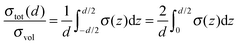
The conductivity and diffusivity data of thin film and multilayer studies with different layer thicknesses cannot be compared directly. Comparing the value for the bulk transport with the highest measured values for thin film samples, as it is reported in an experimental study, can be misleading. The measured (total) conductivity σtot or diffusivity Dtot of a sample depends essentially on the layer thickness d. In the simple case of independent and parallel transport through the bulk phase(s) of the ionic conducting film(s) and along the phase boundaries the following expression can be derived:6,48| |
 | (1) |
Ion conducting films with two interface regions with a width of δ0′ each and a constant conductivity σint are assumed. The bulk region with a thickness d − 2δ0′ has the unchanged volume conductivity σvol. The layer thickness d must be larger than 2δ0′. An analogous expression can be derived for the corresponding diffusivities Dtot, Dvol and Dint.12,13
By plotting the measured (total) conductivity σtot or diffusivity Dtot of the samples divided by the bulk value vs. the reciprocal layer thickness 1/d one obtains (in a first approximation) a linear relation, once the interface regions do not overlap. The effect of the interfaces on the total ionic transport can be characterised by the slope factor sσ ≡ 2δ0′(σint/σvol − 1), respectively, sD ≡ 2δ0′(Dint/Dvol − 1), independently of the prepared layer thicknesses. Both factors sσ and sD should be identical and their values can be directly compared, due to the Nernst–Planck relation (see in detail in Section 4).
2.2 Classification of the experimental data from the literature
The magnitudes of the slope factors sσ and sD in Table 1 evaluated from the published data differ by about eight orders of magnitude. Because of a non-linear behaviour, the slope factors for some of the studies vary considerably when including the data for the thinnest investigated layer thicknesses. In this case we specify two values, together with the evaluated layer thickness range. In the case of studies where only one measurement for a single thickness is given, the slope factor is italicised.
Considering the material properties of the used ionic conductors, the morphology and the structure of the hetero-interfaces we classify all studied systems into three groups according to the magnitude of the slope factors:
(i) Strain control: multilayers consisting of extrinsic ionic conductors (and insulators).5,6,9,11–13,24,49–51 The slope factors have a value of about 101 nm at maximum.
(ii) Surface control: single thin films/multilayers consisting of an extrinsic ionic conductor, exhibiting an open surface.8,10,14,44–48 The value of the slope factors is above 101 nm and about 105 nm at maximum.
(iii) Space charge control: multilayers consisting of intrinsic ionic conductors.53,55,57,59 A slope factor in the order of 103 nm can be observed.
There is clear evidence that the highest increase of the ionic conductivity observed in the study of Garcia et al.5 of up to eight orders of magnitude in ultra-thin and strained YSZ films is rather due to effects on electronic conduction than to an increased ionic mobility.61–63 Comparing the reported sample properties and experimental conditions, it is possible to attribute the observed interface effects in each group to a distinct (most probable) mechanism.
Space charge regions as an origin for increased interface transport can be attributed to group (iii) for systems with intrinsic ionic conductors. A slope factor in the order of 103 nm can be found. These considerably high values result from the low conductivity of intrinsic bulk materials and a relatively strong conductivity increase in the space charge region. Thus, even with this increase the total conductivity σtot remains low compared to the bulk conductivity of extrinsic ionic conductors.
In group (i) for systems with extrinsic ionic conductors the smallest effects on the interface transport appear. The (absolute) values of the slope factors are only in the order of 101 nm. Because of the absence of space charge regions, only strain fields, misfit dislocations or disordered transition regions in solid–solid phase boundaries may cause these moderate effects. The grain boundary density may easily have a conductivity effect in the same order of magnitude, however, often reducing the conductivity. Thus, strain effects may then not increase the conductivity relative to single crystalline material, but may help to reduce the negative effect of blocking grain boundaries. We emphasise that the influence of grain boundaries depends on the size of the film crystallites. Unfortunately, information on the film microstructure is not given in all cited references.
In group (ii) also systems with extrinsic ionic conductors can be found, but with slope factors above 101 nm and at maximum up to 105 nm. This can be explained by open surfaces of the ion conducting phases as a common feature of all samples. Atomic transport along surfaces (solid–gas interfaces) is usually much faster compared to grain or phase boundary transport (solid–solid interfaces). The decreased number of bonds of a surface atom and reconstruction phenomena will considerably change the activation energy for jump processes.64 For the majority of the experimental studies attributed to this group a slope factor in the order of 102 nm can be found, i.e. one order of magnitude higher compared to group (i).
In the following, we will perform an analytical treatment of the elastic strain effects occurring in category (i) on a phenomenological basis using linear transport theory. Aim is an analytical expression for the ionic conductivity or the diffusion coefficient of interfacially strained nano-/microscaled thin films, consisting of ionic conducting and insulating phases. A correlation between the transport parameters and the dimensions of the ionic conducting layers and the mutual mismatch between the adjacent phases are derived and compared with available experimental data. A simplified treatment has already been published by us in previous papers.9,24 Major improvement of our model is the introduction of a grain boundary dependent strain relaxation in the solid electrolyte films, describing the thin films in a more realistic way.
3 Phenomenological model for strain effects
3.1 Lattice mismatch and elastic strain
A thin film (multilayer) model system is considered. It is assumed that the adjacent layers consist of two crystalline phases, 1 and 2. Both thin film materials are elastically deformable. There is a lattice mismatch due to different lattice constants but the interfaces are still coherent:| |
 | (2) |
Hereby, f1/2 is the mismatch of phase 1 relative to phase 2 and f2/1 the mismatch of 2 relative to 1. The mismatch between phase 1 and 2 is assumed to be small, typically below ±5%. In mechanical equilibrium a common lattice distance dhkl,0 in the interface plane is reached, if both phases are elastically deformable:| |
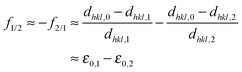 | (3) |
3.2 Elastic strains and stresses
The thin films of the ionic conducting phase consist of columnar crystallites. As depicted in Fig. 1, the direction perpendicular to the interface planes is defined as the z-axis and parallel to it as x- and y-axes. For the further considerations the phase indices 1 and 2 are dropped. Each crystallite has two phase boundary planes at z = −d/2 and z = d/2, i.e. a height d (= layer thickness). A biaxial strain state is assumed. The strain due to the mismatch is only applied at the phase boundaries in the x–y-plane. The diameter of the crystallites in the phase boundary planes in x- and y-directions has the width l. The elastic properties in both phases are assumed to be similar. The interface strain will be divided approximately in equal parts by both adjacent phases:
| | |
f1/2 ≈ −f2/1 ≈ 2ε0,1 = −2ε0,2 = 2ε0
| (4) |
If the diameter of adjacent crystallites is relatively small, the interface strain in both phases can be relaxed by local deformation in regions close to the interfaces. Thus, in each crystallite two interface regions with a spatially decaying strain are formed. To obtain the function describing the decay of the elastic deformation one has to solve an integral equation, which connects the elastic deformation, respectively, the resulting strain and stress with the total elastic energy of the system. The desired function is obtained by minimising the total elastic energy of the system, i.e. for mechanical equilibrium.
 |
| | Fig. 1 Elastically deformable crystallites of phase 1 with a diameter l and a height d (layer thickness). The tensile strained case is shown in (a) and the compressively strained case in (b). The lattice planes are matched across the interface to the crystallites of phase 2 (not shown). Elastic strain relaxation by local deformation took place in the vicinity of both interfaces by introduction of dislocations in the grain boundaries. The spatial extent of the strained interface regions is proportional to δ0. | |
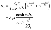
As a simple approximation an exponential decay for the elastic deformation can be assumed. Murakami et al., Luryi et al., Stoica et al. and Fischer et al. also apply exponential strain relaxation for the description of elastic strain states in epitaxially grown and island shaped crystallites on silicon substrates.65–69 Due to this, the thickness limit for the formation of coherent interfaces is increased.64,70 The volume elements in each layer may be elastically shifted only parallel to the x- and the y-axis, see Fig. 1. To compensate the interface mismatch by an elastic deformation ±lε0/2 the shifts ux and uy will increase linearly with the distance from the x–z-plane, respectively, the y–z-plane. For x = 0 the shift in the x-direction is zero and for y = 0 the shift in the y-direction is zero. The maximum shift for a volume element in a layer is reached in the phase boundary planes at z = −d/2 and z = d/2 at the outer limits x = ±l/2 and y = ±l/2 of the crystallite. The shift uz in the z-direction depends only on the distance from the x–y-plane.
The strain fields originating from the phase boundary planes will superpose, if the height d of the crystallite is small. The resulting elastic deformations at the phase boundary planes at z = −d/2 and z = d/2 cannot exceed the deformation xε0/2 required to compensate the interface mismatch. For an exponential decay of the elastic deformation, these conditions are satisfied by the following functions (∝ ez/δ0−d/2δ0, ∝ e−z/δ0−d/2δ0, scaling factor of 1 + e−d/δ0):
| |
 | (5) |
| |
 | (6) |
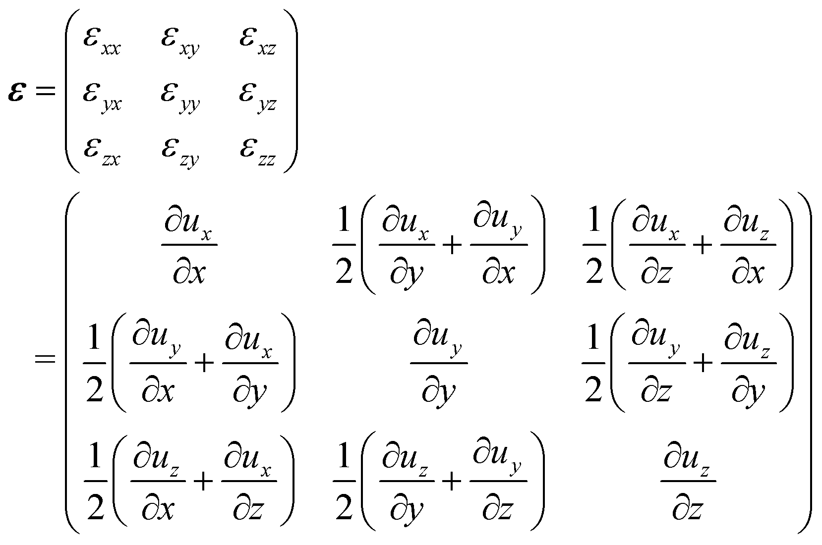
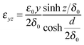
The parameter δ0 describes the width of the strained interface region (decay of the deformation by a factor of 1/e). From the elastic deformations in eqn (5) to (7) the strain components εxx, εyy, εzy, εzx and εxy can be calculated:†
| |
 | (9) |
| |
 | (10) |
| |
 | (11) |
In Fig. 2 the profile of the biaxial strain εxx and εyy is depicted vs. the position on the z-axis. As a boundary condition, there are no (external) forces perpendicular to the phase boundary planes, i.e. the stress component σzz is zero:
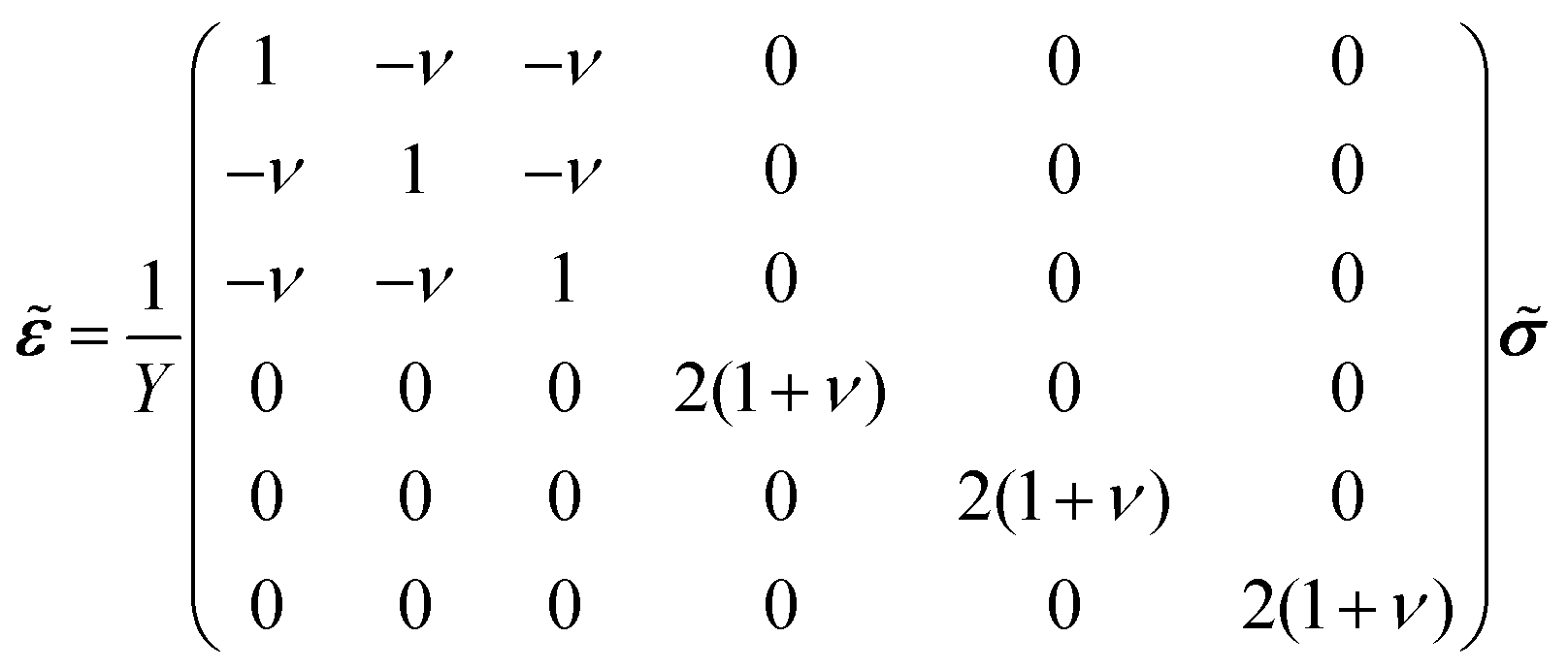
The stress components σxx, σyy, σyz, σxz and σxy as well as the strain component εzz are obtained from eqn (9) to (13) using the generalised Hooke's law:‡
| |
 | (15) |
| |
 | (16) |
| |
 | (17) |
| |
 | (19) |
For the sake of simplicity of the theoretical treatment, an isotropic system is assumed, which can be described only by two elastic constants, Young's modulus
Y and the Poisson ratio
ν. The system has ideal elastic properties,
i.e. the interface strain leads only to elastic distortion of the interface regions. We ignore more complex effects of mechanically induced lattice transformation or changes in the short-range order of ions.
71
 |
| | Fig. 2 Profile of the relative biaxial strains εxx/ε0 and εyy/ε0vs. the relative position 2z/d. The phase boundaries are situated at 2z/d = −1 and 1. Curves are plotted for different ratios d/2δ0 between layer thickness and the extent of the strained interface region. Noticeable overlap of the strain fields appears, if d/2δ0 < 5. | |
3.3 Total elastic energy, width of the strained interface regions
The value of the parameter δ0, describing the spatial extent of the strained region in mechanical equilibrium, can be gained by minimising the total elastic energy Eelast of the system:| |
 | (20) |
Inserting all strain and stress components from eqn (9) to (19) in eqn (20) and performing an integration within the boundaries from x = −l/2…l/2, y = −l/2…l/2 and z = −d/2…d/2 one gets:| |
 | (21) |
The minimum of the elastic energy Eelast can be found by derivation of eqn (21) with respect to δ0 and setting equal to zero. Only one solution is physically meaningful:| |
 | (22) |
Within the limits of this model the width δ0 of the elastically strained interface regions depends directly on the diameter l of the crystallites. Typical values for the Poisson ratio ν of ceramic materials are in the range between 0.3 and 0.4, i.e. δ0 is about 13% to 15% of the diameter l of the crystallites.
3.4 Local (isotropic) pressure
The corresponding local isotropic pressure p can be calculated from the stress components σxx, σyy and σzz in eqn (15) to (13):§| |
 | (24) |
At the phase boundary planes, z = ±d/2, the local isotropic pressure reaches its maximum value:| |
 | (25) |
3.5 Local ionic conductivity
The diffusion coefficient D and the ionic conductivity σ of O2−-ions are pressure dependent. For simplification, we focus on extrinsic ionic conductors with oxygen vacancies  as the predominant mobile defect. Assuming an activated jump process one obtains according to the transition state theory:
| |
 | (26) |
If we can neglect the pressure dependence of local point defect equilibria on the vacancy concentration  , the differentiation of eqn (26) in respect to the pressure p yields:
| |
 | (27) |
The pressure dependence of the geometric factor β, the jump distance λ, the concentration c of oxide ions and the Debye frequency (∼ω0) is also not taken into account.72 In this case the pressure induced change of transport coefficients in eqn (27) depends only on the activation volume ΔV# of the migrating point defect.
As depicted in Fig. 3 only ionic transport parallel to the phase boundaries will be considered. The value of the ionic conductivity for the unstrained volume phase (for p = 0) will be denoted σvol and the value of the diffusion coefficient of the unstrained volume phase Dvol. To obtain an expression for the local ionic conductivity σ(z) as a function of the position z perpendicular to the phase boundary planes, eqn (27) has to be integrated within the limits σvol…σ(z) and 0…p(z). The same applies to obtain an expression for the local diffusion coefficient D(z):
| |
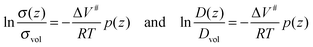 | (28) |
As long as only relative values in relation to the unstrained bulk are considered, the expressions to treat ionic conductivity and the diffusion coefficient have an identical form. Thus, in the following only the expression for the ionic conductivity will be shown for brevity. By inserting the local pressure
p(
z) from
eqn (28) into
eqn (24) one yields:
| |
 | (29) |
The dimensionless parameter
α combines all material constants, as Young's modulus
Y, the Poisson ratio
ν and the activation volume Δ
V# for the atomic jumps.
 |
| | Fig. 3 Parallel conduction σvol in the volume (bulk) and along interface regions close to the phase boundary with a modified conductivity σint. | |
3.6 The total conductivity as an average between strained and unstrained regions
The total conductivity σtot perpendicular to the z-axis can be calculated as an integral average of the local conductivity σ(z) within the limits z = −d/2…d/2 (see Fig. 3):| |
 | (30) |
By inserting eqn (29) in eqn (30) an expression for the total conductivity σtot relative to the volume conductivity σvol of a thin film with the thickness d can be derived:| |
 | (31) |
By introducing a dimensionless film thickness parameter d* = d/2δ0 and a new integration variable z′ = z/δ0 the integral in eqn (31) can be simplified:| |
 | (32) |
To obtain analogue expressions for the diffusion coefficient, in eqn (32) and all following equations only σtot(d*)/σvol has to be substituted with Dtot(d*)/Dvol.
Unfortunately, there is no analytical solution for integrals of the type ∫exp[acosh(t)]dt. In Fig. 4 numerically calculated values for the relative ionic conductivity σtot/σvol are plotted vs. the reciprocal film thickness parameter 1/d*, using typical values of αε0 for ceramic thin film systems.
 |
| | Fig. 4 Solid lines: relative ionic conductivity σtot/σvol according to eqn (32)vs. the reciprocal film thickness parameter 1/d* (= 2δ0/d). Dashed lines: initial slopes and limiting interface conductivities. For the parameter αε0 typical values found in ceramic thin films are used (Y = 200 GPa, ν = 0.3, T = 823 K, ΔV# = 2.0 cm3 mol−1 and ε0 = −1.8%…2.2%). | |
3.7 Limit for very thick layers
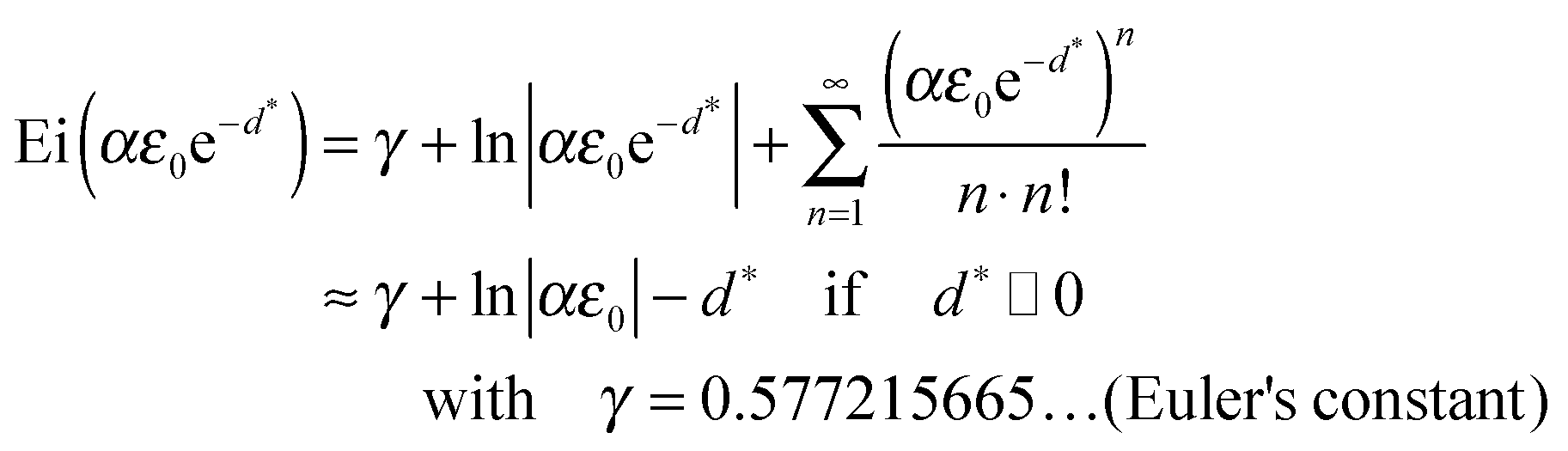
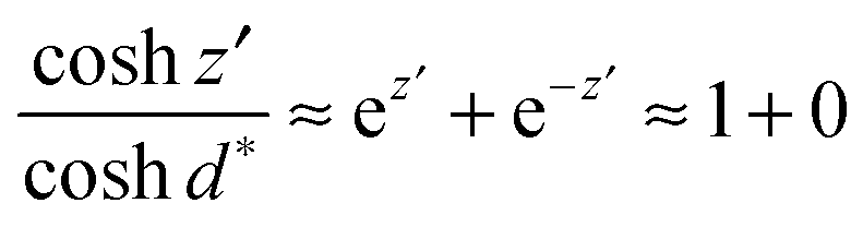
In the case of “thick” films any superposition of the interface strain fields is negligible. The integral in eqn (32) can be approximated,¶ if d ≫ 2δ0, i.e. d* ≫ 1:| |
 | (34) |
The integral in eqn (34) of the type ∫exp[aexp(t)]dt can be solved analytically:||| |
 | (36) |
For the limit d* ≫ 1 further simplifications can be made:**| |
 | (38) |
Thus, eqn (32) can be approximated with a linear relation. The initial slope Ei(αε0) − ln|αε0| − γ depends only on the parameter α and the mismatch induced elastic strain ε0. For infinitely thick films d* → ∞, eqn (38) and thus eqn (32) will reach a limiting value of 1, i.e. interfacial strain is negligible for geometrical reasons.
Ionic conductivity or diffusivity data, evaluated from experimental studies, as compiled in Table 1, can only be plotted directly vs. the reciprocal film thickness 1/d, as δ0 is not known a priori:
| |
 | (39) |
In a plot of
σtot/
σvol or
Dtot/
Dvolvs. 1/
d the width of the strained interface region
δ0 is part of the initial slope 2
δ0[Ei(
αε0) − ln|
αε0| −
γ]. Thus, the measured initial slope depends also on the diameter
l of the film crystallites, see
eqn (22). In
Fig. 5 the relative ionic conductivity
σtot/
σvol for
αε0 = 1.0 and a Poisson ratio
ν = 0.3 is plotted for typical values of the crystallite diameter
l, found in vacuum deposited thin films.
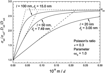 |
| | Fig. 5 Solid lines: relative ionic conductivity σtot/σvol according eqn (32)vs. the reciprocal film thickness 1/d for typical values of the diameter l of the crystallites in the thin film (αε0 = 1.0 and ν = 0.3). Dashed lines: initial slopes and limiting interface conductivity. | |
Clearly, not only the film thickness d but also the crystallite morphology within the layers is an important parameter, influencing the strain effect on ionic transport. The shape of the crystallites, i.e. the ratio between height (identical with film thickness) d and diameter l controls the volume fraction of the strained interface regions relative to the unstrained bulk, see eqn (22). For the same film thickness d, the strain effect on interface transport increases with increasing diameter l of the crystallites. However, if the diameter of the crystallites decreases in the same proportion as the layer thickness, l ∼ d, the effect cancels out and the overall transport coefficients σtot and Dtot remain constant (2δ0/d = const.).
3.8 Limits for very thin layers
In the case of very thin films the elastic strain fields, originating from both phase boundaries, overlap to a large extent. The integral in eqn (32) can be approximated,†† if d ≪ 2δ0, i.e. d* ≪ 1:| |
 | (41) |
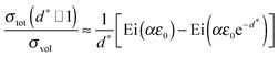
Thus, eqn (32) will reach a limiting value of eαε0. As well as the initial slope for very thick layers, the limiting value of the relative ionic conductivity σtot/σvol for very thin layers only depends on the parameter α and the mismatch induced elastic strain ε0 (see Fig. 4).
Directly at the phase boundaries the maximum isotropic pressure and thus the maximum effect on the local ionic transport should be expected. Consequently, the limiting value σtot(d* ≪ 1) in eqn (41) can be defined as the (maximum) interface ionic conductivity σint:
| |
 | (42) |
3.9 An approximation function for the relative ionic conductivity
There is no analytical solution for the parametric integral in eqn (32). An approximation function can be given, by combining the limiting values for very thin and very thick layers:‡‡| |
 | (44) |
The function in eqn (44) is a good approximation for lattice mismatches below 10%, using values of the material constants typically found in ceramic ionic conductors. The highest derivations are found in the intermediate range for d* ≈ 1.
4 Discussion
In the following we will discuss and compare the experimental studies from the literature5,11,49–51 and own studies6,9,12,13,24,60 performed on extrinsic oxide ion conductors from category (i), as summarised in Table 1, with the improved strain model. In these studies the total ionic conductivity σtot and diffusion coefficient Dtot for oxide ion transport in multilayers consisting of the extrinsic conductor YSZ are measured parallel to the phase boundaries, as described by the strain model (see Fig. 3). For a proof of the introduced theoretical model on a quantitative—and not only on a qualitative level—the basic assumption limiting its applicability has to be considered. Only studies using systems with plain, parallel orientated and coherent films can be quantitatively discussed.
In the studies from the literature and own studies, summarised in Tables 1 and 2, the ionic transport in the multilayer and thin film samples is always measured parallel to phase boundaries. The total O2−-conductivity is determined by impedance spectroscopy and the O2−-diffusion coefficients by 18O-tracer experiments. For an extrinsic ionic conductor like YSZ or CGO, the relative change of the ionic conductivity σtot/σvol (to the bulk value) is identical to the relative change of the diffusion coefficient of the mobile ions Dtot/Dvol, if there is no additional electronic conduction:§§
| |
 | (45) |
In an extrinsic ionic conductor, the concentration of mobile charge is virtually constant due to the high doping concentration. Thus, the concentration of mobile O
2−-ions close to the phase boundaries should be essentially the same as in the bulk phase,
ctot ≈
cvol. For this reason, the relative changes in the transport parameters
σtot/
σvol and
Dtot/
Dvol for O
2−vs. the reciprocal film thickness 1/
d are comparable and can be combined and plotted in the same diagram (see
Fig. 7).
Table 2 Own experimental studies on (0001) Al2O3/RE2O3/[YSZ/RE2O3] × n multilayers (RE = Lu, Sc and Y). The mismatch is calculated for a commensurate relation of 2:1 of the unit cell parameter (aYSZ:aRE2O3). The width δ0 of the strained interface region is determined by non-linear curve fitting, using eqn (43), the value of the parameter α and the data plotted in Fig. 7. RSD is the standard deviation of δ0, calculated from the residue. The (average) diameters l of the film crystallites are calculated according to eqn (22), using the fit parameter δ0. The initial slopes are (a) calculated according to eqn (39) and (b) determined by linear regression of the onset of the plotted data
| Multilayer system |
f YSZ/RE2O3/% |
Experimental studies |
Temperature/°C |
Fit using eqn (43) |
Initial slope/nm |
| α/1 |
δ 0/nm |
RSD/nm |
l/nm |
Eqn (39) |
Lin. regr. |
| YSZ/Sc2O3 |
−4.37 |
Conductivity9 |
560 |
53.4 |
4.4 |
0.1 |
32 |
−7.9 |
−6.1 ± 0.8 |
| Diffusion13 |
550 |
54.0 |
6.3 |
0.1 |
46 |
−11.4 |
−8.5 ± 0.2 |
| |
| YSZ/Lu2O3 |
1.02 |
Conductivity24,60 |
560 |
53.4 |
(−0.3) |
0.3 |
(−2.1) |
(−0.17) |
−1.4 ± 2.4 |
| Diffusion |
Not measured |
| |
| YSZ/Y2O3 |
3.04 |
Conductivity6 |
560 |
53.4 |
3.7 |
0.01 |
27 |
7.4 |
7.4 ± 0.1 |
| Diffusion12 |
520 |
56.1 |
7.1 |
0.2 |
51 |
15.3 |
12.9 ± 0.9 |
4.1 Material parameters of YSZ
In the case of a pure strain based effect on the interface transport, the magnitude of the expected increase (or decrease) of the total ionic conductivity and diffusivity and thus the slope in a σtot/σvol or Dtot/Dvolvs. 1/d plot can be estimated, using eqn (39). The value of the dimensionless parameter α can be calculated solely from literature data for the elastic properties and activation volume:
Activation volume of YSZ. Park et al. have measured a value of 2.08 cm3 mol−1 for the activation volume ΔV# of YSZ (9.5 mol% Y2O3).73 The experimental study was performed at 750 °C, applying uniaxial pressure. This is in accordance with other studies on (extrinsic) fluorite type anionic conductors,74–81 providing typically values of 2–4 cm3 mol−1. The activation volume ΔV# is strongly dependent on the lattice structure. Rock salt type ionic conductors have generally higher values in the range of 6–10 cm3 mol−1.72,82
Elastic properties of YSZ. The model is derived for a material with isotropic elastic properties. The elastic parameters for cubic YSZ, Young's modulus Y and the Poisson ratio ν, change considerably with the crystallographic direction.83–85 Moreover, Young's modulus is also temperature dependent.84–90 The isotropic (average) Young's modulus of YSZ doped with 10 mol% Y2O3 decreases considerably from 210 GPa to 167 GPa in the temperature range between 25 and 400 °C. The Poisson ratio does only change slightly from 0.36 to 0.37:89
| Temperature/°C |
25 |
400 |
450 |
500 |
550 |
600 |
| Young's modulus/GPa |
210 |
167 |
167 |
168 |
168 |
169 |
| Poisson ratio |
0.36 |
0.37 |
0.37 |
0.37 |
0.37 |
0.36 |
At room temperature in the doping range from 5 to 15 mol% Y2O3 there is no pronounced composition dependence of the elastic parameters.85,91 At higher temperatures also a considerably composition dependence can be noticed. Thus, for temperatures between 400 and 600 °C we calculate values between 65.7 and 50.4 for the parameter α.
4.2 Experimental studies on YSZ multilayers from the literature
The maximum misfit observed in experimental studies on polycrystalline thin films, respectively, multilayers with columnar crystallite structure and (quasi-)coherent phase boundaries may not exceed 6 to 10%. The average crystallite sizes of films prepared by gas phase deposition are typically in the range of 20 to 100 nm. The highest misfits will only be reached in thin films, consisting of (columnar) crystallites with a very small diameter. According to eqn (42), this results in an increase of the interface transport coefficients compared to the bulk value of about 10 at maximum, but in the case of such small crystallites the effect of blocking grain boundaries will also be maximised. The maximum slope as defined in eqn (39) may not exceed values of sσ = 30 nm.
Unfortunately, a detailed and quantitative discussion of all experimental studies from the literature in category (i) is not possible. In the case of the studies of Karthikeyan et al. on multilayer samples, consisting of random orientated YSZ films and amorphous insulating layers, it is difficult to estimate the actual interface strain.49 In the studies of Pergolesi and Li et al. multilayers consisting of two ionic conductors with comparable O2−-conductivity were used.11,51 If a misfit is relaxed by tensile strain in the first ion conducting phase and by compressive strain in the second phase, as assumed in our model, the increased transport in the first phase will be (partially) canceled out or overcompensated by the decreased transport in the second phase (or vice versa). The resulting effect on the total conductivity or the diffusion coefficient may depend on the ratio of the elastic properties, the activation volumes as well of the layer thicknesses. In spite of the problem that no definite estimation can be made, all measured slopes of the studies from category (i) are in the expected range below sσ = 30 nm.
In the case of the experimental study of Pergolesi et al. the phase boundaries of the used YSZ/CeO2-multilayer samples were also heavily rugged.51,92 Mismatch induced coherency strain can be reduced by introduction of misfit dislocations but also by tilting of the interface planes. This may be the cause why any strain effect is suppressed (despite 5.2% misfit) and why the authors observe no conductivity effect.
There is only one exceptional study with an extraordinary large effect with a slope in the order of 108 nm. As discussed in the beginning this is probably a misinterpretation of the effects caused by electronic conduction or experimental issues.61–63
4.3 Own experimental studies on the YSZ/rare earth metal oxide multilayer
Preparation of model systems. Due to the lack of experimental studies which allow a quantitative evaluation of the strain state in the interface, we have performed own studies on multilayers consisting of cubic fluorite-type YSZ and ionic transport blocking cubic bixbyite-type rare earth metal sesquioxides.6,9,12,13,24,60 The bixbyite structure (Ia![[3 with combining macron]](https://www.rsc.org/images/entities/char_0033_0304.gif) ) is closely related to the fluorite structure (Fmm). Essentially, the bixbyite unit cell has twice the lattice parameter of the fluorite unit cell. Only 2/3 of the original fluorite anion lattice sites are occupied. In our recent studies multilayer samples with different rare earth metal sesquioxides RE2O3 with RE = Lu, Sc and Y were prepared by pulsed laser deposition on (0001) Al2O3 substrates. YSZ with a doping level of 9.5 mol% Y2O3 was used. The lattice parameter of the used bixbyite-type rare earth metal sesquioxide RE2O3 and the fluorite-type YSZ have approximately a 2:1 ratio. An overview of the experimental studies is given in Table 2.
) is closely related to the fluorite structure (Fmm). Essentially, the bixbyite unit cell has twice the lattice parameter of the fluorite unit cell. Only 2/3 of the original fluorite anion lattice sites are occupied. In our recent studies multilayer samples with different rare earth metal sesquioxides RE2O3 with RE = Lu, Sc and Y were prepared by pulsed laser deposition on (0001) Al2O3 substrates. YSZ with a doping level of 9.5 mol% Y2O3 was used. The lattice parameter of the used bixbyite-type rare earth metal sesquioxide RE2O3 and the fluorite-type YSZ have approximately a 2:1 ratio. An overview of the experimental studies is given in Table 2.The samples were prepared by pulsed laser deposition (PLD) and characterised by SEM, TEM/SAED and XRD/pole figure measurements. Despite the considerable mismatch between YSZ, Y2O3, and Sc2O3, in the phase boundaries of these multilayers, respectively, only very few mismatch dislocations are formed. Dislocations are located only in and close to the grain boundaries. The phase boundaries in these studies are flat on an atomic level and can be treated as (quasi-)coherent with an ideal 1:1 match of the lattice plains. By changing the rare earth metal sesquioxide, i.e. the lattice parameter, the mutual mismatch fZrO2/RE2O3 can be systematically varied. Thus, the chosen combination of cubic oxides can be used as (nearly) ideal model systems to study strain based effects.
As seen in Fig. 6, the crystallites in all prepared multilayers have only constrained diameters below 100 nm. Thus, the interface strain can be considerably relaxed by local deformation. The average crystallite sizes of all samples are in the same range (see below). Using (0001) Al2O3 substrates, the crystallites in the thin films of the YSZ/Y2O3- and YSZ/Sc2O3-multilayer have only one preferential orientation, (111) YSZ/(111) RE2O3 (RE = Y, Sc). In the case of a YSZ/Lu2O3-multilayer also other orientations like (110) YSZ/(110) Lu2O3 and (100) YSZ/(100) Lu2O3 were found. Details of the experimental setup and the characterisation are given in the cited studies.
 |
| | Fig. 6 Dark field (DF) TEM micrographs of Al2O3/RE2O3/(YSZ/RE2O3) × n multilayers. (a) YSZ/Y2O3 with n = 3, (b) YSZ/Sc2O3 with n = 50 and YSZ/Lu2O3 with n = 70 YSZ layers.6,9,60 All multilayers show a columnar microstructure. The (average) diameter of the crystallites is below 100 nm. | |
4.4 Fitting of the data of own experimental studies
The relative conductivity and diffusion data in Fig. 7 can be fitted with the approximation function in eqn (43) to validate the introduced model. The material dependent parameter α of YSZ for the experimental temperatures is calculated from literature data89 and also listed in Table 2. The only fitting parameter is the width δ0 of the strained interface region.
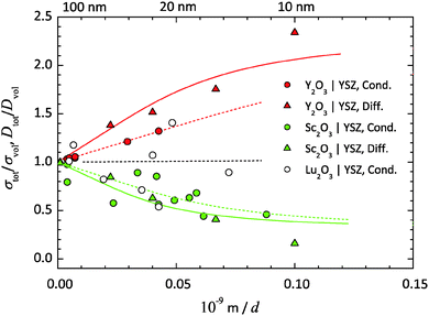 |
| | Fig. 7 Relative O2−-conductivity and diffusion coefficients, σtot/σvol and Dtot/Dvol, from the YSZ/RE2O3-multilayer studies (RE = Y, Lu, Sc) listed in Table 2vs. the reciprocal thickness 1/d of the YSZ layers. The blue and red curves are fitted to the data, using eqn (32) and the values for the parameter α in Table 2. | |
YSZ/Y2O3. The lattice parameters of YSZ (9.5 mol% Y2O3) amount to 5.143 Å and of Y2O3 to 10.604 Å.93–98 Due to the positive lattice mismatch of +3.04%, a tensile strain ε0 of +1.52% relative to the YSZ layers should exist. The relative ionic conductivity and the diffusion coefficient, σtot/σvol and Dtot/Dvol, are increasing with decreasing layer thickness d (increasing density of interfaces). Thus, the initial slopes are positive. As expected from eqn (28), tensile strain results in an increased ionic transport coefficient in the interface region compared to the bulk. An increasing effect of tensile strain on the interface conductivity in extrinsic O2−-conductor is also clearly demonstrated by Li et al. and Sanna et al. for YSZ/GZO and YSZ/SDC multilayers.11,50 By fitting eqn (43)δ0 yields as 3.7 nm for the conductivity data and as 7.1 nm for the diffusion data. Using eqn (22) the (average) diameter l of the film crystallites can be calculated from δ0. For the conductivity data one gets an (average) diameter of 27 nm and for the diffusion data of 51 nm.
YSZ/Sc2O3. The lattice parameter of Sc2O3 equals 9.846 Å.99 Due to the negative lattice mismatch of −4.37% there is a compressive strain ε0 of −2.19% relative to the YSZ layers. As expected for compressive strain in the interfaces a decrease of the ionic conductivity and the diffusion coefficient has been measured. The initial slopes are negative. A decreasing effect of compressive interface strain on conductivity is also shown by Shen et al. for the YDC/CZO multilayer.15 By fitting, δ0 yields 4.4 nm for the conductivity data and 6.3 nm for the diffusion data. The (average) diameter l of the film crystallites results 32 nm for the conductivity data and 46 nm for the diffusion data.
YSZ/Lu2O3. The lattice parameters of Lu2O3 equal 10.391 Å.100,101 The small positive lattice mismatch of +1.02% and thus the only small tensile strain ε0 of +0.52% should result to the least effect on phase boundary transport. Indeed, no clear trend can be seen, due to the strong scattering of the present conductivity data. A simple linear regression of the data yields a negative slope. By fitting eqn (43), δ0 will converge to a small but negative value, because of the specified positive strain. Due to the lack of accuracy of the experimental data, the obtained values for YSZ/Lu2O3 (marked with round brackets) have no physical meaning. At the moment there are no diffusion data available.
Diameter of film crystallites from TEM. The average size of the columnar film crystallites of the multilayer samples can also be estimated from (HR)TEM investigations. This yields values for the film crystallite diameter l in the order of 25–75 nm for the YSZ/Y2O3-multilayer, respectively, in the order of 20–50 nm for the YSZ/Sc2O3-multilayer, see Fig. 6(a) and (b).6,9 The smaller grain size is measured close to the Al2O3 substrate, the larger in the middle of the multilayer. Thus, the values for l determined by fitting the conductivity data of about 30 nm and by fitting the diffusion data of about 50 nm are close to the values from the microscopic investigations.In the case of the YSZ/Lu2O3-multilayers the diameter l cannot be determined by fitting because of the strong scattering of the present conductivity data. From (HR)TEM investigations values between 20 and 70 nm were determined for the (average) diameter l of the YSZ crystallites,24,60 which are comparable to the values obtained for YSZ/Y2O3- and YSZ/Sc2O3-multilayers, see Fig. 6(c).
4.5 Partial electronic conduction
In the case of stoichiometric composition, bulk phase rare earth sesquioxides Y2O3, Sc2O3 and Lu2O3 are insulators for ionic and electronic transport6,9,24,60 and bulk phase YSZ is virtually a pure ionic conductor with a negligible electronic transfer number. For thin film or multilayer samples, additional electronic conductivity due to a partial reduction of the bulk phases or a change of the electronic band structure in the interface region is discussed.63,102 Also experimental artefacts originating from external short-circuit paths are often considered, but can be safely excluded in the case of our multilayers—as their resistance is always much lower than the resistance of the substrate and sample holder.61,62
The absence of electronic partial conductivity can be verified by comparing the results of the ionic conductivity with 18O-tracer diffusion measurements.12,13 In a diffusion experiment only ionic transport is measured. In a conductance experiment a possible electronic partial conductivity may be included in the total conductivity. In all of our studies σtot/σvol is equal or at least smaller than Dtot/Dvol. One can conclude that neither a significant electronic partial conduction nor leakage currents through the substrate or the ceramic sample holder play a measurable role. This holds as long as there is no strong variation of the (average) crystallite diameter and no depletion of mobile oxygen vacancies in the interface region, which might overcompensate an increase of the total conductivity caused by additional electronic conduction.
4.6 Grain boundaries
The grain boundaries between the crystallites in ionic conducting layers may influence the total ionic conductivity of the multilayer. Depending on the mutual orientation of adjacent crystallites, i.e. on the grain boundary structure (from low angle to high angle grain boundaries), ionic transport across (perpendicular) the grain boundaries is often hampered compared to the bulk.103
In addition to the blocking effect at grain boundaries also additional non-equilibrium lattice defects, like local disordered regions or dislocation loops in the volume of the crystallites, can reduce the measured total ionic transport. Such lattice defects can locally influence the point defect equilibria and alter the migration enthalpy.104,105 In the case of thin films, non-equilibrium lattice defects in particular originate from the vapour deposition techniques used for preparation. Such defects can only relax if sufficient diffusional (cationic and anionic) transport through the volume is possible. This can be safely achieved at a preparation temperature or a subsequent heat treatment above 1/2 to 3/4 of the melting point Tmelt.106,107 All multilayers were subjected to a heat treatment at 800 before performing the measurements. This is only 1/3 of the melting temperature of YSZ (∼2700 °C).
The blocking effect of grain boundaries and additional non-equilibrium lattice defects within the crystallites in micro-/nanocrystalline films can reduce the mean ionic transport coefficients—compared to (bulk) single crystal samples—by up to one order of magnitude. Depending on the grain orientation and the degree of the film texture even anisotropic conductivity can be expected. By and large, conductivity effects caused by the texture, grain boundary structure and non-equilibrium lattice defects may be in the same order of magnitude as strain-based effects at hetero-phase boundaries. We emphasise that our model in Section 3 describes only the strain effect caused by hetero-phase boundaries. Any other blocking effect has to be treated separately. This is perfectly reasonable, as the (absolute) conductivity of the bulk film does not represent a model parameter—we only scale the strain effect by comparison with the film bulk conductivity.
In essence, a prerequisite for the reproducible investigation of strain effects are multilayer samples with a comparable texture, grain boundary density and lattice defect density in the crystallites. The ionic conductivity for unstrained regions of the films is in fact reduced compared to a single crystal, but should be roughly sample independent. This can be only achieved if all samples are prepared with the same deposition technique, using well reproducible conditions. As described before, in the case of (own) experimental studies on YSZ/RE2O3 multilayers this could be assured by using always the same deposition parameters for PLD preparation, the same heat treatment before performing the ionic transport measurements, and by subsequent XRD and TEM analysis.9,12,13,48
By analysing the results from the improved strain based model, one finds that the (average) diameter l of the crystallites in the ion conducting layers on its own is a crucial parameter in addition to the layer thickness d, determining the extent of the strain effect on ionic transport. The (average) diameter of the crystallites directly influences the strain relaxation in the interface regions, i.e. the width of the strained region δ0 and thus the measured initial slopes, see eqn (22). By combining eqn (39) with eqn (22) one finds:
| |
 | (46) |
In multilayer samples with a decreasing (average) diameter
l of the film crystallites as a function of the layer thickness
d,
i.e. with a linear dependence like
l ∼
d, the geometric dependence on the measured total transport properties disappears or will be diminished.
4.7 Point defect association equilibria
In heavily doped extrinsic ionic conductors like YSZ or CGO the mobile oxygen vacancies can form associates with the immobile dopant cations, which are charged relative to the regular cations. In the case of YSZ, the formation of { } pairs has then to be considered, which depends on the Y2O3 doping level:
| |
 | (47) |
In the presented model in Section 3 the mismatch induced strain is linked in a kinetic first-order approach with the ionic conductivity only by the pressure dependence of the free activation enthalpy ΔG# for ion jumps, see eqn (26), which governs the rate of successful jumps. The concentration of mobile point defects is assumed to be constant. When taking point defect equilibria into account, as eqn (47), pressure, respectively, pressure gradients, can influence the concentration of mobile oxygen vacancies  . The defect association equilibrium in eqn (47) can be described by a mass action law with an equilibrium constant Kass and a free reaction enthalpy ΔG0ass:
| |
 | (48) |
In the case of strong association, i.e. and
and  , eqn (48) can be approximated to:
| |
 | (49) |
By inserting eqn (49) in (26) the pressure dependence of the ionic conductivity and the diffusion coefficient can be easily calculated. The influence of strain on the conductivity σ is now controlled by sum of the activation volume ΔV# for the ionic motion and the reaction volume ΔV0ass of point defect association:| |
 | (50) |
The result for the diffusion coefficient D is analogue. There are only very few experimental studies available providing data for the reaction volume of point defect association.108–111 Positive as well as negative values can be found. A reaction volume ΔV0ass in the order of −9 cm3 mol−1 is estimated for the formation of { } ion pairs in CGO.109,110 Thus, association effects may either enhance or diminish the effect of strain on ionic jumps.
In the case of weak association, i.e. and
and  , eqn (48) can be approximated to:
| |
 | (51) |
Hereby,

is the total concentration of Y
3− dopant cations. If

, point defect association can be neglected and the pressure dependence of the concentration of mobile oxygen vacancies

will tend to zero. If the value of
Kass has the same magnitude as

, the pressure dependence in the case of weak association is smaller compared to strong association. We assume that association effects can be neglected in this case, anyhow.
Clearly, mere transport experiments do not allow us to separate the effects of strain on defect mobility and on the concentration of mobile defects. But one should keep in mind that the effect on the concentration of mobile vacancies can be significant, once association is severe. The values of ΔV# and ΔV0ass can be of comparable magnitude and can either add up or cancel out.
We also like to add that the segregation of dopants or impurities in the vicinity of grain and phase boundaries may have an effect. In heavily doped extrinsic ionic conductors like YSZ or CGO the doping components Y2O3, Gd2O3, respectively, are often accumulated in the interfaces, depending on the preparation conditions.112,113 As state above, we could not find evidence for significant segregation at hetero-phase boundaries prepared by PLD, and therefore, we exclude it from further discussion. However, the possibility should be kept in mind, and under prolonged high temperature treatment segregation may occur even driven by local strain.
5 Conclusions/summary
5.1 Phenomenological model and model experiments
We introduce a theoretical model for the description of the ionic transport in strained polycrystalline ceramic thin films and multilayers, consisting of a solid electrolyte and an insulator. It is based on interface strain fields, originating from phase boundaries with a structural mismatch. Assuming exponentially decaying strain fields, an analytical expression is obtained for the ionic conductivity/ionic diffusion coefficient relative to the bulk phase, as a function of the film thickness. The resulting formula depends only on the elastic parameters, the activation volume and the diameters of the crystallites in the film layers, see eqn (32). Thus, it is of general character.
We also performed a literature survey to compile a summary of the recent experimental studies on anion (O2− and F−) transport in thin films and multilayers. The studies can be categorised by introducing the “slope factor” sσ, which numerically describes the influence of the increasing phase boundary density on the conductivity. The least effect in the order of 101 nm at maximum can be found for systems consisting of extrinsic ionic conductors. Higher effects above 101 nm up to about 105 nm at maximum can be observed if surface transport is included. Systems consisting of intrinsic conductors range in the order of 103 nm. We like to note that the apparently small strain effects in category (i) may be of greater practical significance than space charge effects in category (iii). Space charge effects will only be observed in systems with small intrinsic conductivity, where the resulting conductivity can still be much lower than in extrinsic, strongly doped electrolytes. Thus from a practical point of view, strain effects can be important in improving electrolytes with high conductivity.
Strain or structural effects are probably the origin of the modified interface transport properties for systems consisting of extrinsic ionic conductors. In the case of pure strain effects the observed magnitudes are in the predicted range of the model. Due to the typical elastic properties of ceramic oxides and structural limitations for coherency strain, the strain effect will only affect interface transport properties less than a factor of 10. However, a factor of 10 is a significant increase for an electrolyte which already has a high conductivity. However, as already pointed out above, grain boundaries in strained epitaxial films will also influence the ionic conductivity – mostly in the direction of a lower conductivity. The effective total conductivity will then depend on the balance between grain boundary and strain effects. Maximal strain effects will be found in thin films with large columnar grains, where the density of grain boundaries is low and strain relaxation is not very effective. This is a highly important result, and we conclude that real “strain design” of solid electrolytes from the first requires advanced thin film deposition techniques with controlled growth of wide area epitaxial films with coarse grains.
In own studies, YSZ/rare earth metal oxide multilayers with coherent interfaces and various mismatches and thus interface strain were used. The experimentally observed dependence of the transport properties (relative to the bulk) vs. layer thickness can be fitted to the model, only using literature data for the elastic parameters and activation volume. The only fit parameter is the (average) diameter of the film crystallites. The values obtained from fitting are in accordance with the values determined by TEM. The model is able to explain on a semi-qualitative level the observed effects on interface transport.
The results from the conductivity measurements on the YSZ/Lu2O3 multilayer samples scatter considerably. The most important difference compared to the YSZ/Y2O3- and YSZ/Sc2O3-multilayers is a less well defined texture/orientation of the film crystallites. This will cause additional and different types of grain boundaries between the crystallites in a layer, which may also change the ionic transport coefficient to a different extent.
To verify the influence of interface strain, still more experimental data for ionic conduction and diffusion in multilayer systems with well defined geometry and texture are required. In addition to the transport measurements also an X-ray diffraction analysis on the directional strain fields in the layers has to be performed. The functional course of the measured (average) strain perpendicular and parallel to the phase boundaries in the solid electrolyte and the insulator phase as a function of the layer thickness can be used to support the basic assumptions of the model.
5.2 Limitations of a simple strain based model
It comes out that strain effects will only influence the ionic transport in a layered system (of solid electrolytes with a high concentration of mobile charge carriers) at maximum by one order of magnitude. Grain boundaries in the bulk of the ion-conducting layers influence the total conductivity in the same order of magnitude due to their blocking effect on ionic transport. Thus, only samples with similar grain boundary density and texture may be safely compared to explore the role of strain effects. The (average) diameter of the crystallites is in addition to the layer thickness also a crucial parameter determining the influence of the strain effects on ionic transport. According to the model, the (average) diameter of the crystallites directly controls the strain relaxation in the interface regions and thus the measured initial slopes.
Our model is based on isotropic mechanical behaviour. Only an isostatic pressure is assumed to introduce the pressure dependence of the ionic transport coefficients. This can only be a first order approach to demonstrate the fundamental effect of strain on interface transport. It can be improved by using the full (anisotropic) compliance tensors. The results would depend on the space group, the orientation of the film crystallites and the current direction in the interface plane. As well, the partial derivatives of the free activation enthalpy with respect to the stress components have to be considered separately.
Acknowledgements
We like to thank Dietrich Hesse from the Max-Planck-Institut für Mikrostrukturphysik (Halle/Saale, Germany) for the TEM investigations and many helpful discussions. The author CK likes to thank the DFG for financial support to proceed with the experimental studies. The author JJ acknowledges support by the project STORE-E (LOEWE program funded by the State of Hessen) and LaMa (Laboratory of Materials Science).
References
- L. Blum, H.-P. Buchkremer, S. Gross, A. Gubner, L. G. J. de Haart, H. Nabielek, W. J. Quadakkers, U. Reisgen, M. J. Smith, R. Steinberger-Wilckens, R. W. Steinbrech, F. Tietz and I. C. Vinke, Fuel Cells, 2007, 7, 204–210 CrossRef CAS.
- S. D. Souza, S. J. Visco and L. C. D. Jonghe, Solid State Ionics, 1997, 98, 57–61 CrossRef.
- S. Hui, J. Roller, S. Yick, X. Zhang, C. Decès-Petit, Y. Xie, R. Maric and D. Ghosh, J. Power Sources, 2007, 172, 493–502 CrossRef CAS PubMed.
- J. G. Swallow, W. H. Woodford, Y. C. Q. Lu, J. J. Kim, D. Chen, Y.-M. Chiang, W. C. Carter, B. Yildiz, H. L. Tuller and K. J. V. Vliet, J. Electroceram., 2014, 32, 3–27 CrossRef CAS.
- J. Garcia-Barriocanal, A. Rivera-Calzada, M. Varela, Z. Sefrioui, E. Iborra, C. Leon, S. J. Pennycook and J. Santamaria, Science, 2008, 321, 676–680 CrossRef CAS PubMed.
- C. Korte, A. Peters, D. Hesse, N. Zakharov and J. Janek, Phys. Chem. Chem. Phys., 2008, 10, 4623–4635 RSC.
- N. Schichtel, C. Korte, D. Hesse and J. Janek, Phys. Chem. Chem. Phys., 2009, 11, 3043–3048 RSC.
- M. Sillassen, P. Eklund, N. Pryds, E. Johnson, U. Helmersson and J. Bøttiger, Adv. Funct. Mater., 2010, 20, 2071–2076 CrossRef CAS.
- N. Schichtel, C. Korte, D. Hesse, N. Zakharov, B. Butz, D. Gerthsen and J. Janek, Phys. Chem. Chem. Phys., 2010, 12, 14596–14608 RSC.
- K. M. Kant, V. Esposito and N. Pryds, Appl. Phys. Lett., 2012, 100, 033105 CrossRef PubMed.
- B. Li, J. Zhang, T. Kaspar, V. Shutthanandan, R. C. Ewing and J. Lian, Phys. Chem. Chem. Phys., 2013, 15, 1296 RSC.
- H. Aydin, C. Korte, M. Rohnke and J. Janek, Phys. Chem. Chem. Phys., 2013, 15, 1944–1955 RSC.
- H. Aydin, C. Korte and J. Janek, Sci. Technol. Adv. Mater., 2013, 14, 035007 CrossRef.
- J. Jiang, X. Hu, W. Shen, C. Ni and J. L. Hertz, Appl. Phys. Lett., 2013, 102, 143901 CrossRef PubMed.
- W. Shen, J. Jiang and J. L. Hertz, RSC Adv., 2014, 4, 21625–21630 RSC.
- A. Kushima and B. Yildiz, J. Mater. Chem., 2010, 20, 4809–4819 RSC.
- J. A. Hirschfeld and H. Lustfeld, Phys. Rev. B: Condens. Matter Mater. Phys., 2011, 84, 224308 CrossRef.
- G. Dezanneau, J. Hermet and B. Dupé, Int. J. Hydrogen Energy, 2012, 37, 8081–8086 CrossRef CAS PubMed.
- R. A. de Souza, A. Ramadan and S. Hörner, Energy Environ. Sci., 2012, 5, 5445 CAS.
- J. A. Hirschfeld and H. Lustfeld, Phys. Rev. B: Condens. Matter Mater. Phys., 2014, 89, 014305 CrossRef.
- B. Yildiz, MRS Bull., 2014, 39, 147–156 CrossRef CAS.
- D. S. Aidhy, Y. Zhang and W. J. Weber, J. Phys. Chem. C, 2014, 118, 4207–4212 CAS.
- M. Burbano, D. Marrocchelli and G. W. Watson, J. Electroceram., 2014, 32, 28–36 CrossRef CAS.
- C. Korte, N. Schichtel, D. Hesse and J. Janek, Monatsh. Chem., 2009, 140, 1069–1080 CrossRef CAS PubMed.
- J. Santiso and M. Burriel, J. Solid State Electrochem., 2011, 15, 985–1006 CrossRef CAS PubMed.
- J. L. M. Rupp, Solid State Ionics, 2012, 207, 1–13 CrossRef CAS PubMed.
- S. Schweiger, M. Kubicek, F. Messerschmitt, C. Murer and J. L. M. Rupp, ACS Nano, 2014, 8, 5032–5048 CrossRef CAS PubMed.
- J. Laurencin, G. Delette, F. Lefebvre-Joud and M. Dupeux, J. Eur. Ceram. Soc., 2008, 28, 1857–1869 CrossRef CAS PubMed.
- A. Hughes and S. Badwal, Solid State Ionics, 1991, 46, 265–274 CrossRef CAS.
- G. S. A. M. Theunissen, A. J. A. Winnubst and A. J. Burggraaf, J. Mater. Sci., 1992, 27, 5057–5066 CrossRef CAS.
- S. P. S. Badwal, F. T. Ciacchi, S. Rajendran and J. Drennan, Solid State Ionics, 1998, 109, 167–186 CrossRef CAS.
- M. de Ridder, R. G. van Welzenis, A. W. D. van der Gon, H. H. Brongersma, S. Wulff, W.-F. Chu and W. Weppner, J. Appl. Phys., 2002, 92, 3056–3064 CrossRef CAS PubMed.
- C. Chung, K. V. Hansen and M. Mogensen, Ceram. Eng. Sci. Proc., 2004, 25, 407 CAS.
- J. Maier, J. Electrochem. Soc., 1987, 134, 1524–1535 CrossRef CAS PubMed.
- J. Maier, Solid State Ionics, 1994, 70–71, 43–51 CrossRef CAS.
- S. Jiang and J. B. Wagner, J. Phys. Chem. Solids, 1995, 56, 1101–1111 CrossRef CAS.
- S. Jiang and J. B. Wagner, J. Phys. Chem. Solids, 1995, 56, 1113–1124 CrossRef CAS.
- J. Maier, Solid State Ionics, 1995, 75, 139–145 CrossRef CAS.
- J. Maier, Prog. Solid State Chem., 1995, 23, 171–263 CrossRef CAS.
- H. Tuller, Solid State Ionics, 2000, 131, 143–157 CrossRef CAS.
- J. Maier, Solid State Ionics, 2000, 131, 13–22 CrossRef CAS.
- J. Maier, J. Eur. Ceram. Soc., 2004, 24, 1251–1257 CrossRef CAS.
- J. Maier, Solid State Ionics, 2004, 175, 7–12 CrossRef CAS PubMed.
- I. Kosacki, C. M. Rouleau, P. F. Becher, J. Bentley and D. H. Lowndes, Electrochem. Solid-State Lett., 2004, 7, A459–A461 CrossRef CAS PubMed.
- I. Kosacki, C. M. Rouleau, P. F. Becher, J. Bentley and D. H. Lowndes, Solid State Ionics, 2005, 176, 1319–1326 CrossRef CAS PubMed.
- S. Azad, O. A. Marina, C. M. Wang, L. Saraf, V. Shutthanandan, D. E. McCready, A. El-Azab, J. E. Jaffe, M. H. Engelhard, C. H. F. Peden and S. Thevuthasan, Appl. Phys. Lett., 2005, 86, 131906 CrossRef PubMed.
- A. Karthikeyan, C.-L. Chang and S. Ramanathan, Appl. Phys. Lett., 2006, 89, 183116 CrossRef PubMed.
- A. Peters, C. Korte, D. Hesse, N. Zakharov and J. Janek, Solid State Ionics, 2007, 178, 67–76 CrossRef CAS PubMed.
- A. Karthikeyan and S. Ramanathan, J. Appl. Phys., 2008, 104, 124314 CrossRef PubMed.
- S. Sanna, V. Esposito, A. Tebano, S. Licoccia, E. Traversa and G. Balestrino, Small, 2010, 6, 1863–1867 CrossRef CAS PubMed.
- D. Pergolesi, E. Fabbri, S. N. Cook, V. Roddatis, E. Traversa and J. A. Kilner, ACS Nano, 2012, 6, 10524–10534 CAS.
- D. Lubben and F. A. Modine, J. Appl. Phys., 1996, 80, 5150–5157 CrossRef CAS PubMed.
- N. Sata, K. Eberman, K. Eberl and J. Maier, Nature, 2000, 408, 946–949 CrossRef CAS PubMed.
- S. Furusawa and T. Kawaguchi, J. Phys. Soc. Jpn., 2001, 70, 3585–3590 CrossRef CAS.
- N. Sata, N. Y. Jin-Philipp, K. Eberl and J. Maier, Solid State Ionics, 2002, 154–155, 497–502 CrossRef CAS.
- F. Shin-ichi, S. Satoshi, S. Kaduhiro and T. Hitoshi, Solid State Ionics, 2004, 167, 325–329 CrossRef CAS PubMed.
- N. Y. Jin-Phillipp, N. Sata, J. Maier, C. Scheu, K. Hahn, M. Kelsch and M. Rühle, J. Chem. Phys., 2004, 120, 2375–2381 CrossRef CAS PubMed.
- N. Kuwata, N. Sata, T. Tsurui and H. Yugami, Jpn. J. Appl. Phys., Part 1, 2005, 44, 8613–8618 CrossRef CAS.
- X. Guo and J. Maier, Adv. Funct. Mater., 2009, 19, 96 CrossRef CAS.
- N. Schichtel, C. Korte, D. Hesse, N. Zakharov and J. Janek, Phys. Chem. Chem. Phys., 2015 Search PubMed , to be published.
- H.-R. Kim, J.-C. Kim, K.-R. Lee, H.-I. Ji, H.-W. Lee, J.-H. Lee and J.-W. Son, Phys. Chem. Chem. Phys., 2011, 13, 6133–6137 RSC.
- X. Guo, Scr. Mater., 2011, 65, 96–101 CrossRef CAS PubMed.
- A. Cavallaro, M. Burriel, J. Roqueta, A. Apostolidis, A. Bernardi, A. Tarancón, R. Srinivasan, S. N. Cook, H. L. Fraser, J. A. Kilner, D. W. McComb and J. Santiso, Solid State Ionics, 2010, 181, 592–601 CrossRef CAS PubMed.
- A. P. Sutton and R. W. Balluffi, Interfaces in Crystalline Materials, Clarendon Press, 1995 Search PubMed.
- M. Murakami, Thin Solid Films, 1980, 69, 253–267 CrossRef CAS.
- A. Fischer, Cryst. Res. Technol., 1983, 18, 1415–1422 CrossRef CAS.
- S. Luryi and E. Suhir, Appl. Phys. Lett., 1986, 49, 140–142 CrossRef CAS PubMed.
- T. Stoica and L. Vescan, J. Cryst. Growth, 1993, 131, 32–40 CrossRef CAS.
- A. Fischer, H. Kühne, B. Roos and H. Richter, Semicond. Sci. Technol., 1994, 9, 2195–2198 CrossRef CAS.
- D. Hull and D. J. Bacon, Introduction to Dislocations, Butterworth–Heinemann, Oxford, 3rd edn, 1997, vol. 37 Search PubMed.
- J. Kreisel, M. C. Weber, N. Dix, F. Sánchez, P. A. Thomas and J. Fontcuberta, Adv. Funct. Mater., 2012, 22, 5044–5049 CrossRef CAS.
- M. Beyeler and D. Lazarus, Z. Naturforsch., A: Phys. Sci., 1971, 26, 291–299 CAS.
- E. T. Park and J.-H. Park, Proceedings of the 3rd International Meeting of Pacific Rim Ceramic Societies, Kyungju, Korea, 1998.
- J. Oberschmidt and D. Lazarus, Phys. Rev. B: Condens. Matter Mater. Phys., 1980, 21, 5813–5822 CrossRef CAS.
- J. Oberschmidt and D. Lazarus, Phys. Rev. B: Condens. Matter Mater. Phys., 1980, 21, 2952–2961 CrossRef CAS.
- J. Oberschmidt and D. Lazarus, Phys. Rev. B: Condens. Matter Mater. Phys., 1980, 21, 5823–5834 CrossRef CAS.
- S. Matar, J. Réau, G. Demazeau, C. Lucat, J. Portier and P. Hagenmuller, Solid State Commun., 1980, 35, 681–684 CrossRef CAS.
- P. Hagenmuller, J.-M. Réau, C. Lucat, S. Matar and G. Villeneuve, Solid State Ionics, 1981, 3/4, 341–345 CrossRef.
- D. R. Figueroa, J. J. Fontanella, M. C. Wintersgil, A. V. Chadwick and C. G. Andeen, J. Phys. C: Solid State Phys., 1984, 17, 4399–4411 CrossRef CAS.
- C. Varotsos, M. Lazaridou and P. Varotsos, Phys. Rev. B: Condens. Matter Mater. Phys., 1985, 32, 2634–2635 CrossRef CAS.
- I. V. Murin, O. V. Glumov, W. Gunsser and M. Karus, Radiat. Eff. Defects Solids, 1995, 137, 251–254 CrossRef CAS.
- M. Beyeler and D. Lazarus, Solid State Commun., 1969, 7, 1487–1489 CrossRef CAS.
- N. G. Pace, G. A. Saunders, Z. Sümengen and J. S. Thorp, J. Mater. Sci., 1969, 4, 1106–1110 CrossRef CAS.
- H. M. Kandil, J. D. Greiner and J. F. Smith, J. Am. Ceram. Soc., 1984, 67, 341–346 CrossRef CAS PubMed.
- R. P. Ingel and D. Lewis III, J. Am. Ceram. Soc., 1988, 71, 265–271 CrossRef CAS PubMed.
- J. W. Adams, R. Ruh and K. S. Mazdiyasni, J. Am. Ceram. Soc., 1997, 80, 903–908 CrossRef CAS PubMed.
- A. Selçuk and A. Atkinson, J. Eur. Ceram. Soc., 1997, 17, 1523–1532 CrossRef.
- S. Giraud and J. Canel, J. Eur. Ceram. Soc., 2008, 28, 77–83 CrossRef CAS PubMed.
- T. Kushi, K. Sato, A. Unemoto, K. Amezawa and T. Kawada, ECS Trans., 2009, 25, 1673–1677 CAS.
- T. Kushi, K. Sato, A. Unemoto, S. Hashimoto, K. Amezawa and T. Kawada, J. Power Sources, 2011, 196, 7989–7993 CrossRef CAS PubMed.
- S. Hart, J. Wallis and I. Sigalas, Physica B, 1986, 139 & 140, 183–186 Search PubMed.
- D. Pergolesi, M. Fronzi, E. Fabbri, A. Tebano and E. Traversa, Mater. Renewable Sustainable Energy, 2013, 2, 1–9 CrossRef.
- W. Baukal and R. Scheidegger, Ber. Dtsch. Keram. Ges., 1968, 45, 610–616 CAS.
- M. Moringa and J. Cohen, Acta Crystallogr., Sect. A: Found. Crystallogr., 1979, 35, 789–795 CrossRef.
- M. Yashima, S. Sakasi, M. Kakihana, Y. Yamaguchi, H. Arashi and M. Yoshimura, Acta Crystallogr., Sect. B: Struct. Sci., 1994, 50, 663–672 Search PubMed.
- M. Paton and E. N. Maslen, Acta Crystallogr., 1965, 19, 307–310 CrossRef CAS.
- H. O'Conner and T. Valentine, Acta Crystallogr., Sect. B: Struct. Sci., 1969, 25, 2140–2144 CrossRef.
- H. Ishibashi, K. Shimomoto and K. Nakahigashi, J. Phys. Chem. Solids, 1994, 55, 809–814 CrossRef CAS.
- S. Geller, P. Romo and J. P. Remeika, Z. Kristallogr., 1967, 124, 136–142 CrossRef CAS PubMed.
- H. Bommer, Z. Anorg. Allg. Chem., 1939, 241, 273–280 CrossRef CAS.
- D. H. Templeton and C. H. Dauben, J. Am. Chem. Soc., 1954, 76, 5237–5239 CrossRef CAS.
- K. Song, H. Schmid, V. Sro, E. Gilardi, G. Gregori, K. Du, J. Maier and P. A. van Aken, APL Mater., 2014, 2, 032104 CrossRef PubMed.
- T. Kiguchi, T. J. Konno, H. Funakubo, O. Sakurai and K. Shinozaki, J. Ceram. Soc. Jpn., 2014, 121, 72–77 CrossRef.
- J. L. M. Rupp, B. Scherrer, N. Schäuble and L. J. Gauckler, Adv. Funct. Mater., 2010, 20, 2807–2814 CrossRef CAS.
- J. L. M. Rupp, E. Fabbri, D. Marrocchelli, J.-W. Han, D. Chen, E. Traversa, H. L. Tuller and B. Yildiz, Adv. Funct. Mater., 2014, 24, 1562–1574 CrossRef CAS.
- J. A. Thornton, Annu. Rev. Mater. Sci., 1977, 7, 239–260 CrossRef CAS.
- R. Messier, A. P. Giri and R. A. Roy, J. Vac. Sci. Technol., A, 1984, 2, 500–503 CAS.
- A. N. Papathanassiou and J. Grammatikakis, Phys. Rev. B: Condens. Matter Mater. Phys., 1996, 53, 16247–16251 CrossRef CAS.
- A. Kossoy, Y. Feldman, E. Wachtel, I. Lubomirsky and J. Maier, Adv. Funct. Mater., 2007, 17, 2393–2398 CrossRef CAS.
- A. Kossoy, Y. Feldman, R. Korobko, E. Wachtel, I. Lubomirsky and J. Maier, Adv. Funct. Mater., 2009, 19, 634–641 CrossRef CAS.
- J. A. V. Orman, C. Li and K. L. Crispin, Phys. Earth Planet. Inter., 2009, 172, 34–42 CrossRef PubMed.
- S. Estradé, J. M. Rebled, J. Arbiol, F. Peiró, I. C. Infante, G. Herranz, F. Sánchez, J. Fontcuberta, R. Córdoba, B. G. Mendis and A. L. Bleloch, Appl. Phys. Lett., 2009, 95, 072507 CrossRef PubMed.
- Y. Zhu, A. Chen, H. Zhou, W. Zhang, J. Narayan, J. L. MacManus-Driscoll, Q. Jia and H. Wang, APL Mater., 2013, 1, 050702 CrossRef PubMed.
Footnotes |
† The components of the Cauchy strain tensor ε can be calculated from the elastic deformations:| |
 | (8) |
|
‡ The strain components ![[small epsilon, Greek, tilde]](https://www.rsc.org/images/entities/b_i_char_e0de.gif) = (εxx, εyy, εzz, 2εyz, 2εxz, 2εxy) and the stress components = (εxx, εyy, εzz, 2εyz, 2εxz, 2εxy) and the stress components ![[small sigma, Greek, tilde]](https://www.rsc.org/images/entities/b_i_char_e10d.gif) = (σxx, σyy, σzz, σyz, σxz, σxy) in an isotropic system are connected by the compliance tensor (using Voight notation): = (σxx, σyy, σzz, σyz, σxz, σxy) in an isotropic system are connected by the compliance tensor (using Voight notation):| |
 | (14) |
|
§ The isotropic pressure is determined by the trace of the stress tensor σ:| | |
p = −⅓(σxx + σyy + σzz)
| (23) |
|
¶ If d* ≫ 1 one can approximate coshd* ≈ 1/2ed*. Since the integration variable z′ varies only between 0 and d*, the expression in the exponent of eqn (32) can be simplified:| |
 | (33) |
|
|| Using the exponential integral function  one can derive: one can derive:| |
 | (35) |
|
** A series expansion can be made for the exponential integral function. The infinite sum term can be neglected for small values of the functional argument:| |
 | (37) |
|
†† If |d*| ≪ 1 one can approximate cosh d* ≈ 1. Because, the integration variable z′ varies only between 0 and d* the expression in the exponent of eqn (32) can be simplified to:| |
 | (40) |
|
‡‡ An approximation for the parametric integral  can be found when considering that the hyperbolic cosine converges to 1/2e±t for t → ±∞ and to 1 for t → 0. The slope at x → 0, i.e. can be found when considering that the hyperbolic cosine converges to 1/2e±t for t → ±∞ and to 1 for t → 0. The slope at x → 0, i.e. should be ea. Thus, for x → ±∞ it can be approximated by the exponential integral function and for x → 0 by a linear function: should be ea. Thus, for x → ±∞ it can be approximated by the exponential integral function and for x → 0 by a linear function:| |
 | (43) |
The maximum deviation of this approximation function from the exact solution is about 5%. |
| §§ Considering the Nernst–Planck relation: σi/(ziF)2 = Dici/RT. |
|
| This journal is © the Owner Societies 2014 |
Click here to see how this site uses Cookies. View our privacy policy here. 
 Open Access Article
 This Open Access Article is licensed under a Creative Commons Attribution-Non Commercial 3.0 Unported Licence


 as the predominant mobile defect. Assuming an activated jump process one obtains according to the transition state theory:
 , the differentiation of eqn (26) in respect to the pressure p yields:


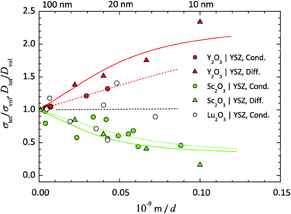

 } pairs has then to be considered, which depends on the Y2O3 doping level:
 . The defect association equilibrium in eqn (47) can be described by a mass action law with an equilibrium constant Kass and a free reaction enthalpy ΔG0ass:
 and
and  , eqn (48) can be approximated to:
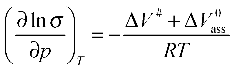
 } ion pairs in CGO.109,110 Thus, association effects may either enhance or diminish the effect of strain on ionic jumps.
 and
and  , eqn (48) can be approximated to:
 is the total concentration of Y3− dopant cations. If
  , point defect association can be neglected and the pressure dependence of the concentration of mobile oxygen vacancies
  will tend to zero. If the value of Kass has the same magnitude as
  , the pressure dependence in the case of weak association is smaller compared to strong association. We assume that association effects can be neglected in this case, anyhow.
 one can derive:
 can be found when considering that the hyperbolic cosine converges to 1/2e±t for t → ±∞ and to 1 for t → 0. The slope at x → 0, i.e.
 should be ea. Thus, for x → ±∞ it can be approximated by the exponential integral function and for x → 0 by a linear function: