 Open Access Article
 This Open Access Article is licensed under a
 Creative Commons Attribution 3.0 Unported Licence
A cracked polymer templated metal network as a transparent conducting electrode for ITO-free organic solar cells†
K. D. M.
Rao
a,
Christoph
Hunger
b,
Ritu
Gupta
a,
Giridhar U.
Kulkarni
*a and
Mukundan
Thelakkat
*b
aChemistry & Physics of Materials Unit and Thematic Unit of Excellence in Nanochemistry, Jawaharlal Nehru Centre for Advanced Scientific Research, Jakkur P.O., Bangalore 560 064, India. E-mail: kulkarni@jncasr.ac.in
bApplied Functional Polymers, Macromolecular Chemistry I, University of Bayreuth, D-95440 Bayreuth, Germany. E-mail: mukundan.thelakkat@uni-bayreuth.de
First published on 9th June 2014
Abstract
We report a highly transparent, low resistance Ag metal network templated by a cracked polymer thin film and its incorporation in an organic solar cell. The performance of this scalable metallic network is comparable to that of conventional ITO electrodes. This is a general approach to replace ITO in diverse thin film devices.
Organic solar cells (OSCs) are an attractive option for large area and inexpensive production of modules. This is because OSCs are well suited to low cost manufacturing due to simple processing1 steps that are easily translated to roll-to-roll mass production2 and lead to near commercialization. In the recent past, extensive research has been carried out on the active semiconductor ingredients3 and electrode optimization4 in order to improve the OSC performance,5 which is typically poorer compared to other types of solar cells such as dye sensitized solar cells6 and silicon based solar cells.7,8 Nonetheless, OSCs occupy a unique position in the photovoltaic roadmap as solid state, flexible, environmentally benign and ultralight large area devices.9
In OSCs, indium tin oxide (ITO) is the most commonly used transparent conducting electrode. Best ITO films exhibit a transmittance of 92% in the visible region and a sheet resistance of 10 ohm □−1.10 Indium is scarce and expensive;11 ITO requires high temperature processing, is brittle and develops cracks on flexible substrates.12 In order to address these issues, there has been much effort towards alternative electrodes, as reported in the literature. Graphene,13 carbon nanotubes (CNTs),14,15 and Ag nanowires16,17 have been proposed as alternatives to ITO. Graphene has outstanding optical properties, but a limited sheet resistance of 30 ohm □−1.13 The CNT networks also exhibit high sheet resistance and in addition, are less stable under ambient conditions.14,18 Ag nanowire networks show relatively superior performance in terms of transmittance and sheet resistance.17 But like any other network produced from pre-synthesized nanowires (tubes), they suffer from contact resistance at innumerable crossbar junctions and high roughness.19,20 Further, the redundant wires/tubes in the network can short the OSCs, which restricts its use in roll-to-roll fabrication. Often, they require an extra treatment, such as mechanical pressing,21 thermal treatment20 or poly(3,4-ethylenedioxythiophene) poly(styrenesulfonate) (PEDOT:PSS) coating to improve the performance.19
Metal grids offer attractive alternatives to the above TCEs.22–30 Indeed being free of junctions, they exhibit high performance in terms of transmittance and sheet resistance, and have been successfully used in optoelectronic devices including OSCs. Typically, they are produced by patterning using lithographic techniques such as photolithography,22 soft lithography,23 phase shift lithography24 and nanoimprint lithography.25 A technologically relevant and simple alternative is the direct printing of grids using silver nanoparticle inks either by ink-jet printing26,27 or laser printing27–29 or flexographic and thermal imprinting.30 These recipes for Ag grids result in relatively large feature sizes. Such printed patterns are often used as current collecting grids in diverse applications.
Recently, metal meshes have been fabricated based on cracked TiO2 templates and their application in touch screens has been shown.31,32 Some of us33 have shown, very recently, selective deposition of Cu by electroplating in the cracked regions of a polymer template to produce Cu mesh based TCEs. These cracked template methods are highly scalable but need to be tested for their applicability and device integration in thin film organic devices such as OSCs, OFETs, etc. One of the basic challenges is to obtain high light transmission maintaining low sheet resistance for such TCEs. Additionally, in thin film devices, the uniformity and connectivity of such meshes are very critical for the reproducibility of such devices.
In this study, we have explored the feasibility of cracking as a tool for the preparation of such metal meshes from inexpensive polymer templates at room temperature and integrating them as TCEs in bulk heterojunction OSCs. Specifically, using a seamless Ag network in the form of a mesh as a replacement for ITO electrodes, several OSCs having an inverted geometry have been made, which exhibited performance comparable to those produced using ITO. We like to note that this work emphasizes the suitability and reproducibility of such an ITO-free TCE in OSCs and not specifically the optimization of efficiency of any kind of device.
The process flow for templating is shown schematically in Fig. 1. First, a crack layer is produced by drying an acrylic based colloidal dispersion on a glass substrate wherein highly interconnected cracks are spontaneously obtained. These U-shaped grooves are complete cracks down to the substrate to be distinguished from incomplete cracks.34 Using the cracked template, the metal (Ag, 55 nm) is deposited by vacuum evaporation and subsequently, the template is washed away with chloroform.
 | ||
| Fig. 1 Schematic illustration of transparent conducting electrode fabrication (a) cracked template (b) deposition of metal on a cracked template and (c) lift-off of the template giving rise to the Ag network based TCE. | ||
As shown in Fig. 2a, the Ag mesostructures on glass appear to be well interconnected throughout the network. The metal fill factor is estimated to be ∼20% with a structural width of ∼2 μm and an average cell size (spacing between the Ag structures) of 20 to 60 μm. The optical profilometric image (1.2 × 0.8 mm2) in Fig. 2b not only reveals the connectivity of the Ag network over a large area but also shows its seamless nature. The surface roughness of the network is estimated to be ∼5 nm while the peak-to-valley roughness, which corresponds to the network thickness, is 55 nm. The SEM image in Fig. 2c shows a junction where the network surface continues to be smooth and the junction itself is seamless unlike crossbar junctions commonly seen in network TCEs made from pre-synthesized Ag nanowires.21 Accordingly, the sheet resistance was found to be ∼10 ohm □−1, which is rather low considering the thickness of only 55 nm. The transmittance of the Ag network was ∼86% at 550 nm (see Fig. 2d) and the overall transmittance is comparable to that exhibited by ITO but, importantly, extends down to the UV region (see the photograph in the inset). ITO, on the other hand, is a good UV absorber.
 | ||
| Fig. 2 Characterization of the Ag network derived TCE: (a) the optical microscope image (transmission mode), (b) the optical profiler image in a 3D view, (c) the SEM image of a network junction and (d) comparison of transmittance spectra of Ag metallic network and ITO. The inset shows the photograph of a Ag network TCE on a glass substrate. | ||
In the next step of solar cell fabrication, the ZnO barrier layer was brought in by decomposing a zinc acetate film at 150 °C in air (see ESI† for experimental details).35 For a proposed thickness of 45 nm of ZnO, the obtained layer was non-uniform and discontinuous (Fig. 3a) as evident from the dark and grey regions, the latter corresponding to the ZnO covered network. Beiley et al. described previously the fabrication of a Ag nanowire–ZnO nanoparticle composite to obtain a semi-transparent top electrode and achieved a good power conversion efficiency (PCE) of 4.3% in PBDTTPD/PC70BM devices.36 Based on this fact, we increased the thickness of the ZnO layer to 95 nm, 135 nm and 230 nm. We observed an increasing degree of covering of the metal network with the increasing thickness of ZnO. For example, in the SEM image of the 135 nm ZnO layer shown in Fig. 3b, the ZnO film is seen to be uniformly submerging the entire Ag network. This is found to be the optimal ZnO thickness required to submerge the 55 nm thick Ag network so as to have reproducible devices without shorting.
 | ||
| Fig. 3 SEM images and schematic illustrations of the Ag network TCE covered with ZnO layer having a thickness of (a) 45 nm and (b) 135 nm. For more SEM images, see the ESI,† Fig. S1. | ||
Four bottom-illuminated inverted photovoltaic cells (5 devices in each) consisting of poly-3-hexylthiophene (P3HT) and phenyl-C61-butyric acid methyl ester (PCBM) were fabricated on a glass substrate, as shown schematically in Fig. 4a using a Ag network derived TCE. The bar graphs of solar cell parameters (Voc, Jsc, FF and PCE) for all four cells with varying thicknesses of the ZnO barrier layer are shown in Fig. 4b. In cell 1, all five devices with a 45 nm ZnO layer were defective due to shorting. For cell 2 with a 95 nm ZnO layer, only two devices were working with moderate efficiencies. On the other hand, for cells 3 and 4 with 135 and 230 nm ZnO barrier layer thicknesses, respectively, all five devices were found to be functioning. Significantly, the five devices with a 135 nm ZnO layer (cell 3), showed uniform performance with an average efficiency of 2.26 ± 0.05%, while those with a 230 nm ZnO layer exhibited some variations in performance with lower efficiency (1.34 ± 0.43%, see Fig. 4b).
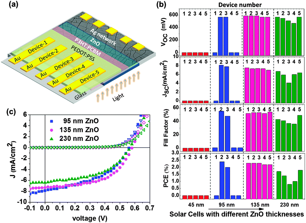 | ||
| Fig. 4 (a) Schematic illustration of the inverted P3HT–PCBM solar cell with Ag network TCE, (b) bar graph of cell parameters for solar cells of different ZnO layer thicknesses (45, 95, 135 and 230 nm), (c) examples of J–V characteristics of solar cells with different ZnO layer thicknesses in the dark (open symbols) and in light (filled symbols). Note that the best performing solar cell is chosen from each cell. | ||
The decrease in the cell efficiency for higher ZnO thicknesses can be attributed to higher series resistance of the cell leading to lower current density and fill factor values (see Fig. 4b).35 Indeed, the variations in solar cell parameters among the five devices exhibit a similar trend. The J–V characteristics of typical solar cells with different ZnO layer thicknesses (95 nm, 135 nm, and 230 nm) are shown in Fig. 4b (see the ESI,† Fig. S2 for J–V characteristics of all working devices).
From Fig. 5a, we can compare the J–V characteristics of a typical device fabricated using a Ag network (from cell 3) with that produced using ITO as a TCE (ITO: T = 93% and Rs = 16 ohm □−1). The Ag network cell has an optimum ZnO layer thickness of 135 nm. For ITO devices, the thickness of the ZnO blocking layer was kept at 45 nm which is optimum for an inverted solar cell.35 All other process parameters such as the active layer thickness, top electrode, annealing temperature, etc. were kept the same for all the devices. It is clear from the plot that the Ag network TCE based solar cell follows a similar trend, as the ITO based cell and the derived parameters are quite comparable (see Table 1). Thus, the efficiency of the Ag network TCE based solar cell was 2.14%, while that obtained for ITO based cells under similar ambient conditions was 2.27%.
 | ||
| Fig. 5 Comparison of (a) J–V characteristics and (b) EQE for the optimized Ag network and ITO devices. | ||
| TCE | V oc (V) | J sc (mA cm−2) | FF (%) | PCE (%) | R sh (Ω cm−2) | R s (Ω cm−2)@Voc | R s (Ω cm−2)@Pmax |
|---|---|---|---|---|---|---|---|
| Ag grid | 0.57 | 7.2 | 51.8 | 2.14 | 421 | 8.3 | 49.7 |
| ITO | 0.55 | 7.5 | 55.2 | 2.27 | 413 | 6.7 | 48.6 |
These results presented here clearly demonstrate the potential of the Ag network based TCE as an alternative to ITO in OSCs. However, a slightly thicker ZnO layer is required to cover the Ag network thickness. Since the ZnO is filled in the interstitial domains between the metallic network, it improves the charge collection properties, which is similar to coating a PEDOT:PSS layer as reported for conventional metal grids.19 The external quantum efficiency (EQE) measurements (Fig. 5b) show that the Ag network TCE based cell exhibits slightly less values in the visible region compared to those derived from ITO cells, but in the UV region, the former excels which makes the overall performance similar for both cells. This can be clearly understood from the differences in transmission of the respective electrodes in the UV region (Fig. 2d). The same information can be inferred by comparing the absorption spectra of the two solar cells (ESI,† Fig. S3) with their EQE spectra.
The method developed in this study for the TCE and associated OSC fabrication has several merits. While the present study has focused on only one type of metallic network, its scope of application can be easily extended to other thin layer devices by varying the template thickness and other parameters in the initial stages of crack template formation. Thus, it is possible to obtain TCEs with different network thicknesses and connectivity and importantly with different metals. Here, Ag was used as a typical example since the work function is favorable for P3HT–PCBM solar cells having an inverted geometry. However, it can be replaced with other metals such as Cu, Al, and Pt depending on the need of application. The metal network based TCE used in the present study works as a current collecting grid at a tens of micrometer scale with a metal fill factor of 20%.
Conclusions
In conclusion, we demonstrated the incorporation of a highly transparent and highly conducting Ag metallic network obtained using a cracked polymer template, in a thin film organic solar cell for the first time. The performance of this highly scalable metal network as a TCE is comparable to that of conventional ITO electrodes. This is a general approach to replace ITO in diverse thin film devices. The crack template approach is universal for any type of metal or substrate material.Acknowledgements
The financial support from the EU Project “Largecells” (Grant No. 261936), Department of Science and Technology, Government of India and the Bavarian State Ministry of Science, Research, and Arts for the collaborative Research Network “Solar Technologies go Hybrid” is gratefully acknowledged. G.U.K., R.G. and K.D.M.R. are grateful to Professor C. N. R. Rao for his encouragement. K.D.M.R. thanks UGC for the SRF fellowship and C. H. acknowledges financial support from DFG (GRK 1640).Notes and references
- Y. Sun, G. C. Welch, W. L. Leong, C. J. Takacs, G. C. Bazan and A. J. Heeger, Nat. Mater., 2012, 11, 44 CrossRef CAS PubMed.
- (a) F. C. Krebs, Sol. Energy Mater. Sol. Cells, 2009, 93, 465 CrossRef CAS PubMed; (b) R. Gupta, S. Kiruthika, K. D. M. Rao, M. Jørgensen, F. C. Krebs and G. U. Kulkarni, Energy Technol., 2013, 1, 770 CrossRef; (c) D. Angmo, S. A. Gevorgyan, T. T. Larsen-Olsen, R. R. Søndergaard, M. Hösel, M. Jørgensen, R. Gupta, G. U. Kulkarni and F. C. Krebs, Org. Electron., 2013, 14, 984 CrossRef CAS PubMed.
- L. Bian, E. Zhu, J. Tang, W. Tang and F. Zhang, Prog. Polym. Sci., 2012, 37, 1292 CrossRef CAS PubMed.
- Y. H. Kim, C. Sachse, M. L. Machala, C. May, L. Müller-Meskamp and K. Leo, Adv. Funct. Mater., 2011, 21, 1076 CrossRef CAS.
- T. Ameri, N. Li and C. J. Brabec, Energy Environ. Sci., 2013, 6, 2390 CAS.
- A. Hagfeldt, G. Boschloo, L. Sun, L. Kloo and H. Pettersson, Chem. Rev., 2010, 110, 6595 CrossRef CAS PubMed.
- M. A. Green, K. Emery, Y. Hishikawa, W. Warta and E. D. Dunlop, Prog. Photovoltaics, 2012, 20, 12 Search PubMed.
- J. Yoo, G. Yu and J. Yi, Sol. Energy Mater. Sol. Cells, 2011, 95, 2 CrossRef CAS PubMed.
- M. Kaltenbrunner, M. S. White, E. D. Głowacki, T. Sekitani, T. Someya, N. S. Sariciftci and S. Bauer, Nat. Commun., 2012, 3, 770 CrossRef PubMed.
- H. Kim, C. M. Gilmore, A. Pique, J. S. Horwitz, H. Mattoussi, H. Murata, Z. H. Kafafi and D. B. Chrisey, J. Appl. Phys., 1999, 86, 6451 CrossRef CAS PubMed.
- A. Kumar and C. Zhou, ACS Nano, 2010, 4, 11 CrossRef CAS PubMed.
- D. R. Cairns, R. P. Witte, D. K. Sparacin, S. M. Sachsman, D. C. Paine, G. P. Crawford and R. R. Newton, Appl. Phys. Lett., 2000, 76, 1425 CrossRef CAS PubMed.
- S. Bae, H. Kim, Y. Lee, X. Xu, J. S. Park, Y. Zheng, J. Balakrishnan, T. Lei, H. Ri Kim, Y. I. Song, Y. J. Kim, K. S. Kim, B. Ozyilmaz, J.-H. Ahn, B. H. Hong and S. Iijima, Nat. Nanotechnol., 2010, 5, 574 CrossRef CAS PubMed.
- R. C. Tenent, T. M. Barnes, J. D. Bergeson, A. J. Ferguson, B. To, L. M. Gedvilas, M. J. Heben and J. L. Blackburn, Adv. Mater., 2009, 21, 3210 CrossRef CAS.
- H. Z. Geng, K. K. Kim, K. P. So, Y. S. Lee, Y. Chang and Y. H. Lee, J. Am. Chem. Soc., 2007, 129, 7758 CrossRef CAS PubMed.
- S. De, T. M. Higgins, P. E. Lyons, E. M. Doherty, P. N. Nirmalraj, W. J. Blau, J. J. Boland and J. N. Coleman, ACS Nano, 2009, 3, 1767 CrossRef CAS PubMed.
- D. Kim, L. Zhu, D. J. Jeong, K. Chun, Y. Y. Bang, S. R. Kim, J. H. Kim and S. K. Oh, Carbon, 2013, 63, 530 CrossRef CAS PubMed.
- D. Zhang, K. Ryu, X. Liu, E. Polikarpov, J. Ly, M. E. Tompson and C. Zhou, Nano Lett., 2006, 6, 1880 CrossRef CAS PubMed.
- W. Gaynor, G. F. Burkhard, M. D. McGehee and P. Peumans, Adv. Mater., 2011, 23, 2905 CrossRef CAS PubMed.
- C. Sahin, A. Elif Selen and U. Husnu Emrah, Nanotechnology, 2013, 24, 125202 CrossRef PubMed.
- L. Hu, H. S. Kim, J. Y. Lee, P. Peumans and Y. Cui, ACS Nano, 2010, 4, 2955 CrossRef CAS PubMed.
- (a) J. Zou, H. L. Yip, S. K. Hau and A. K. Y. Jen, Appl. Phys. Lett., 2010, 96, 203301 CrossRef PubMed; (b) D. S. Ghosh, T. L. Chen and V. Pruneri, Appl. Phys. Lett., 2010, 96, 041109 CrossRef PubMed.
- R. Gupta and G. U. Kulkarni, ACS Appl. Mater. Interfaces, 2013, 5, 730 CAS.
- K. Moon Kyu, G. O. Jong, L. Jae Yong and L. J. Guo, Nanotechnology, 2012, 23, 344008 CrossRef PubMed.
- M. G. Kang and L. J. Guo, Adv. Mater., 2007, 19, 1391 CrossRef CAS.
- Y. Galagan, J.-E. J. M. Rubingh, R. Andriessen, C.-C. Fan, P. W. M. Blom, S. C. Veenstra and J. M. Kroon, Sol. Energy Mater. Sol. Cells, 2011, 95, 1339 CrossRef CAS PubMed.
- Y. Galagan, B. Zimmermann, E. W. C. Coenen, M. Jørgensen, D. M. Tanenbaum, F. C. Krebs, H. Gorter, S. Sabik, L. H. Slooff, S. C. Veenstra, J. M. Kroon and R. Andriessen, Adv. Energy Mater., 2012, 2, 103 CrossRef CAS.
- R. Gupta, M. Hösel, J. Jensen, F. C. Krebs and G. U. Kulkarni, J. Mater. Chem. C, 2014, 2, 2112–2117 RSC.
- R. Gupta, S. Walia, M. Hösel, J. Jensen, D. Angmo, F. C. Krebs and G. U. Kulkarni, J. Mater. Chem. A 10.1039/C4TA00301B.
- J. S. Yu, I. Kim, J. S. Kim, J. Jo, T. T. L. Olsen, R. R. Søndergaard, M. Hösel, D. Angmo, M. Jørgensen and F. C. Krebs, Nanoscale, 2012, 4, 6032 RSC.
- B. Han, K. Pei, Y. Huang, X. Zhang, Q. Rong, Q. Lin, Y. Guo, T. Sun, C. Guo, D. Carnahan, M. Giersig, Y. Wang, J. Gao, Z. Ren and K. Kempa, Adv. Mater., 2014, 26, 873 CrossRef CAS PubMed.
- S. Kiruthika, K. D. M. Rao, A. Kumar, R. Gupta and G. U. Kulkarni, Mater. Res. Express, 2014, 1, 026301 CrossRef.
- S. Kiruthika, R. Gupta, K. D. M. Rao, S. Chakraborthy, N. Padmavathy and G. U. Kulkarni, J. Mater. Chem. C, 2014, 2, 2089 RSC.
- (a) J. C. Li, X. Gong, D. Wang and D. C. Ba, Appl. Phys. A: Mater. Sci. Process., 2013, 111, 645 CrossRef CAS; (b) M. A. Niedermeier, G. Tainter, B. Weiler, P. Lugli and P. Muller-Buschbaum, J. Mater. Chem. A, 2013, 1, 7870 RSC.
- D. Gupta, M. M. Wienk and R. A. J. Janssen, Adv. Energy Mater., 2013, 3, 782 CrossRef CAS.
- Z. M. Beiley, M. G. Christoforo, P. Gratia, A. R. Bowring, P. Eberspacher, G. Y. Margulis, C. Cabanetos, P. M. Beaujuge, A. Salleo and M. D. McGehee, Adv. Mater., 2013, 25, 7020 CrossRef CAS PubMed.
Footnote |
| † Electronic supplementary information (ESI) available: Experimental details of device preparation, additional SEM images and J/V curves of devices. See DOI: 10.1039/c4cp02250e |
| This journal is © the Owner Societies 2014 |