
 Open Access Article
 This Open Access Article is licensed under a Creative Commons Attribution-Non Commercial 3.0 Unported Licence
Plasma chemical and chemical functionalization of polystyrene colloidal crystals
L.
Wegewitz
ab,
A.
Prowald
c,
J.
Meuthen
a,
S.
Dahle
a,
O.
Höfft
 *d,
F.
Endres
d and
W.
Maus-Friedrichs
ab
*d,
F.
Endres
d and
W.
Maus-Friedrichs
ab
aInstitut für Energieforschung und Physikalische Technologien, Technische Universität Clausthal, Leibnizstrasse 4, 38678 Clausthal-Zellerfeld, Germany
bClausthaler Zentrum für Materialtechnik, Technische Universität Clausthal, Leibnizstrasse 4, 38678 Clausthal-Zellerfeld, Germany
cEnergieforschungszentrum Niedersachsen, Technische Universität Clausthal, Am Stollen 19A, 38640 Goslar, Germany
dInstitut für Elektrochemie, Technische Universität Clausthal, Arnold-Sommerfeld-Str. 6, 38678 Clausthal-Zellerfeld, Germany. E-mail: o.hoefft@pe.tu-clausthal.de
First published on 18th July 2014
Abstract
Self-assembling systems of colloidal spheres are widely used as templates for the structured deposition of metals and semiconductors. Multilayer samples of ordered polystyrene spheres are prepared by a flow induced process. The subsequent surface activation by a dielectric barrier discharge in oxygen is followed by the fabrication of protecting polysiloxane layers. Electrochemical deposition of copper is used to test the stability of the pre-treated colloidal crystal. The arrangement of the spheres is preserved during the deposition process, due to the polysiloxane layer. The results of the consecutive preparation steps are investigated concerning topographical and chemical changes by atomic force microscopy, scanning electron microscopy and X-ray photoelectron spectroscopy.
1. Introduction
Monodisperse colloidal spheres have found application in biosensors,1 chemical sensors,2 super capacitors,3 optical sensors4 and templates for macroporous structure synthesis5 to mention a few. By self-assembly they arrange in very small dimensions6 and form photonic crystals.5 An overview on preparation and applications of colloidal crystals was given by Cong et al. recently.7 Polystyrene spheres belong to such colloidal materials. These crystals are used for the template-assisted electrodeposition of macroporous materials.8 The use of ionic liquids for such electrodeposition processes9 increases the wettability and thereby improves the resulting macroporous structure. Different metals can be deposited in the interstitial voids, for example gold and platinum,8 palladium and cobalt,10 silver,11 copper,12 iron and nickel,13ruthenium, osmium and rhenium,14 aluminum,15 zinc16 and lithium.17 Normally the spheres are chemically removed after the deposition of the desired material and the macroporous structure is obtained. We previously observed that the formerly ordered spheres are somewhat disordered after deposition of lithium in the interstitial voids. The deposited material seems to ‘push aside’ the polymer spheres or the well ordered spheres ‘move’ during the deposition process resulting in an unordered structure.17 In such cases it would be desirable to stabilize the soft polymer spheres to strengthen the ordered structure. Therefore a method to stabilize the templating structure during deposition is presented in this contribution. Silanization is a simple way to protect surfaces and has been used for decades to manipulate glass ware for electrophoresis applications as well as for chromatographic and macromolecule separations.18 Therefore we tried to find out whether silanization could stabilize the soft polystyrene spheres against metal deposition or reaction with the deposit. For silanization, oxygen functional groups like hydroxyl, carbonyl, etc. are needed at the surface, but none of them are present in polystyrene. Therefore we treated polystyrene spheres with an oxygen plasma in order to create reactive sites for silane coupling. In the second step, we tried to silanize each of the polystyrene spheres in each layer in a way that the voids are still accessible for deposition. Furthermore, to test the stabilization effect of the silanization, we deposited copper electrochemically in the plasma treated templates as well as the silanized templates. Copper is chosen as the material for deposition because of its potential use in lithium batteries. Macroporous metals and semiconductors are suitable electrode materials for those batteries, as the mechanical stress during volume changes occurring in these devices is much smaller.19 Besides the volume changes, another demanding problem arises when metallic lithium is used as anode material. Dendritic growth of metallic lithium can lead to a short circuit and finally to the destruction of the battery.19,20 Structurally stable frameworks of lithium or copper/lithium combinations may be suitable to lower the probability of malfunctions as a consequence of dendritic growth.In this paper we present the results of our investigation for plasma- and chemically treated spheres analyzed by atomic force microscopy (AFM), scanning electron microscopy (SEM) and X-ray photoelectron spectroscopy (XPS).
2. Experimental
The self-assembled polystyrene structures were prepared on polished copper substrates (1 × 2 cm2) which were cleaned in acetone and ethanol in an ultrasonic bath for twenty minutes. The cleaned copper sheets were dipped in a suspension of polystyrene spheres in ethanol (Duke Scientific, d = 600 nm) at 40 °C and pulled out manually as described earlier.17 Comparable flow-induced processes reported in literature result in well defined multilayer colloidal crystals.21 Afterwards the polystyrene-copper-sheet was annealed for 2 hours at 100 °C.Subsequent to the preparation, the polystyrene spheres were exposed to a dielectric barrier discharge (DBD). The DBD is a low-temperature plasma, where the thermodynamic equilibrium is not established during the discharge.22 This is achieved by insulating one or both electrodes with high dielectric constant materials. The plasma treatment proceeds in a preparation chamber (base pressure 5 × 10⁻⁶ Pa) which is directly connected to the UHV analysis system (base pressure 5 × 10⁻⁹ Pa). This ensures unaltered analysis of the plasma induced changes at the surface of the sample as there is no contact with the ambient atmosphere. The discharge develops in the gap (1 mm) between a self-built electrode23 and the sample serving as ground electrode. The plasma system is operated with a high voltage pulse generator (Ingenieurbüro Dr. Jürgen Klein) and delivers 2 W power (pulse duration t = 0.6 μs, repetition rate 10 kHz, peak voltage 11 kV). All plasma treatments were carried out in oxygen (Linde Gas, 99.995%) at a partial pressure of 20![[thin space (1/6-em)]](https://www.rsc.org/images/entities/char_2009.gif) 000 Pa. The gas composition in the preparation chamber is monitored by a quadrupole mass spectrometer (Balzers QMS 112A).
000 Pa. The gas composition in the preparation chamber is monitored by a quadrupole mass spectrometer (Balzers QMS 112A).
After DBD-processing, the spheres were exposed to DMDCS (dimethyldichlorosilane) dissolved in OMCTS (octamethylcyclotetrasiloxane) to produce a protecting layer. Subsequently copper was electrochemically deposited in the spaces between the spheres from the ionic liquid 1-butyl-3-methylimidazolium dicyanamide ([BMIm]DCA) containing 0.2 mol l−1 of the precursor CuCl. The electrochemical cell has been described in a recent publication.17 All deposition experiments were carried out in a glove box (OMNI-LAB from Vacuum-Atmospheres) under argon atmosphere with oxygen and water contents of about 2 ppm. The deposition was done potentiostatically by applying a potential of −0.2 V for 10 min.
To determine topographical and chemical changes at the surface of the polystyrene spheres caused by the different preparation steps, AFM, SEM and XPS were applied. AFM was performed in tapping mode with a Veeco Dimension 3100 SPM. Al-coated silicon cantilevers (NSC15, Mikromasch, tip curvature <10 nm) with typical resonant frequencies of about 325 kHz and spring constants in the range of 40 N m−1 were used. All images consist of 512 lines each containing 512 pixels. They were recorded with a line-scan frequency of 0.5 Hz. SPIP (Image Metrology A/S) was used to depict the AFM images and to calculate the average surface roughness (RMS) according to ISO 4287/1. Since the characterization of larger surface sections, for example to determine cracks or the wide range ordering of the spheres by AFM is time demanding, SEM was applied as complementary method using a Carl Zeiss DSM 982 Gemini.
XPS was performed by combination of a non-monochromatic X-ray source (Specs RQ20/38C) and a hemispherical analyzer (VSW HA100). The photons (AlKα, 1486.6 eV) illuminate the sample surface at an angle of 80° to the surface normal, while the emitted electrons are detected perpendicular to this direction. The energy resolution of the hemispherical analyzer amounts to 2.2 eV for survey spectra at a constant pass energy of 90 eV and 1.1 eV regarding detail spectra at a pass energy of 44 eV.24 All spectra are displayed as a function of binding energy with respect to the Fermi level. Tougaard Universal Polymer (C 1s region) and Shirley (other regions) background corrections were applied before the photoelectron peak areas are mathematically fitted to the data with CasaXPS (Casa Software Ltd.) using Gaussian peak-shapes. The calculation of the chemical composition of the surface region includes the photoelectric cross sections,25 asymmetry parameters26 and inelastic mean free paths from the database by Jablonski and Powell27 as well as the experimentally determined transmission function of the hemispherical analyser (cf. Hesse et al.28).
3. Results and discussion
The topography of the as-deposited PS spheres is shown in Fig. 1. The SEM image (top) indicates that the preparation leads to a multilayer-system of PS spheres with at least 10–12 layers in fcc structure.29 The largest part of the surface is covered by areas where the (111)-plane of the fcc structure is parallel to the substrate surface. The order is disturbed by cracks of different size probably originating from the drying of the multilayer and the imperfect surface of the underlying copper substrate compared to surfaces of silicon wafers or glass substrates. In the upper left corner there is an area exhibiting unordered spheres possibly because of defects introduced during the preparation, which are known to cause wide range distortions in colloidal crystals.29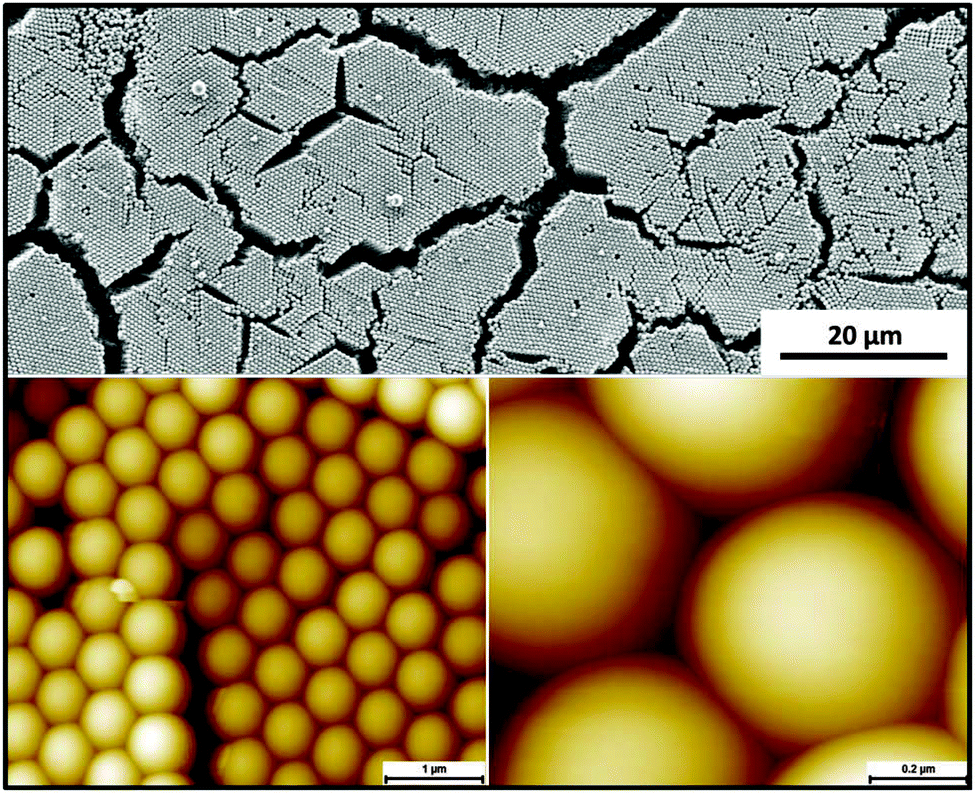 | ||
| Fig. 1 SEM (top) and AFM (bottom) images of as-deposited polystyrene spheres. | ||
In order to inspect the surface of the spheres in detail, AFM is applied, allowing the calculation of the RMS roughness. The calculation refers to sections of the sphere's surface, the corrugation of the crystal lattice is intentionally excluded. This is achieved by subtraction of the sphere curvature. The roughness amounts to Rq = 0.24 nm. Furthermore, the diameter of the spheres can be extracted from the images (577 nm ± 10 nm). The areas free of cracks or deep trenches are about 10–20 μm wide. Additionally, dislocations and point defects (missing spheres) occur. Several methods to produce fcc structures of comparable height with less cracks and a lower defect density exist. For methods based on sedimentation or physical confinement ordered domains of up to 1 cm2 were reported.4,30 However those methods require several hours or days for the template preparation while the flow-induced method used in this work only takes a few minutes. A perfect order of the colloidal template is the crucial factor when producing photonic crystals, but far less decisive for preparing macroporous electrode materials, e.g. for battery applications.
A dielectric barrier discharge in oxygen is applied to the polystyrene template for 60 s. The roughness of the surface exposed to plasma (Rq = 0.24 nm), calculated from Fig. 2, is the same as for the untreated sample. The image shows intact hexagonal arrays of polystyrene spheres after the plasma interaction, indicating that their order is not influenced by the DBD treatment in oxygen. While different researchers report shrinking of the spheres during plasma treatments of several minutes,31–33 the diameter observed here, seems to be stable within the uncertainty (580 nm ± 10 nm). Gogel et al. describe a size reduction of air plasma treated polystyrene spheres.31 After exposing polystyrene spheres to an inductively coupled plasma (ICP) for 60 s, Plettl et al. reported only a slight decrease of the diameter in the range of 2–4%.32 Yan et al. mention a decrease of diameter of 2–3% after one minute of argon plasma treatment.33 Nevertheless, they report that extended treatment times of several minutes led to a significant decrease in size. Those research groups operated their plasma reactors at considerably higher powers (regardless of the process gas) compared to the DBD treatment, which may explain the difference in the observed size changes.
 | ||
| Fig. 2 AFM image of oxygen plasma treated polystyrene spheres. | ||
Contrary to the minor topographical changes after the plasma treatment described above, the surface chemistry is strongly altered by the oxygen DBD. Fig. 3 depicts XPS survey spectra of untreated spheres (a) and plasma treated spheres (b) in comparison. The elements present at the polymer surface are carbon at 285 eV binding energy (the binding energy is charge corrected in all XPS spectra) and oxygen in both cases, while the small molybdenum contribution arises from the sample holder. The untreated spheres exhibit 3.8 at% of oxygen at the surface despite the fact that polystyrene only consists of aromatic and aliphatic carbon as well as hydrogen (which is not detectable by XPS). Impurities are the most probable explanation for the present oxygen contribution on the untreated spheres, where molybdenum oxides from the sample holder yield up to 1/5th of the determined oxygen content as calculated from stoichiometric fractions. As the corresponding spectrum in Fig. 3 illustrates, the amount of oxygen at the surface strongly increases to 21.5 at% due to the DBD treatment.
 | ||
| Fig. 3 XPS survey spectra of as-deposited (a) and oxygen plasma treated (b) polystyrene spheres. | ||
Fig. 4 allows a closer look on the chemical changes at the surface during the plasma treatment focusing on high-resolution spectra of the carbon 1s region prior to any treatment (a) and after application of the DBD (b). Spectrum (a) exhibits three components, the main feature with a shoulder on the high binding energy side (at 286.5 eV) and a satellite peak at 292 eV.
 | ||
| Fig. 4 XPS detail spectra of untreated (a) and of oxygen plasma treated polystyrene spheres (b) depicting the corresponding C 1s regions. | ||
The main peak includes aliphatic and aromatic bound carbon, because the small shift between those peaks does not allow their separation due to the actual resolution of the spectrometer. Merging of aromatic and aliphatic peaks is a reasonable practice for this case.34,35 Surface contamination often occurs in terms of C–O–C or C–OH groups, which explains the shoulder of the main peak. The third component reveals a shake-up structure known to originate from π → π* excitations in the benzene ring separated by 6.8 eV from the main peak. Except for the shoulder, the spectrum resembles literature data very well.34–36 Quantitative information on the chemical composition of the carbon peaks for each preparation step is summarized in Table 1. The estimated errors given in Table 1 have been calculated with CasaXPS based on the mathematical fits of the raw data.
| Untreated | O2 plasma | Polysiloxane coating | Peak shift [eV] | |
|---|---|---|---|---|
| C–C | 80.8 ± 0.9 | 64.6 ± 0.6 | 74.8 ± 0.7 | 0 |
| C–O | 13.2 ± 0.9 | 13.7 ± 0.6 | 12.8 ± 0.7 | +1.5 |
C![[double bond, length as m-dash]](https://www.rsc.org/images/entities/b_char_e001.gif) O O |
6.2 ± 0.6 | 4.5 ± 0.7 | +2.8 | |
| O–CO |
4.8 ± 0.6 | 2.5 ± 0.7 | +4.0 | |
| O–COO |
5.2 ± 0.6 | 2.2 ± 0.7 | +5.2 | |
| Shake up | 6.0 ± 0.9 | 5.5 ± 0.6 | 3.2 ± 0.7 | +6.8 |
Contrary to the three components in the C 1s region of untreated PS spheres, several new components can be identified after DBD treatment in oxygen (see Fig. 4(b)). Due to the limited resolution of the spectrometer it is not possible to separate the new components evolving at the high binding energy side of the C 1s peak after the plasma treatment. To assign the new components, a fitting procedure based on the insights different researchers published for polystyrene films and spheres, exposed to a variety of plasma treatments, is applied.34,35,37 In addition to the main peak and the π → π* shake-up structure, C–O at 286.5 eV, C![[double bond, length as m-dash]](https://www.rsc.org/images/entities/char_e001.gif) O (carbonyl) at 287.8 eV, O–CO (ester) at 289.0 eV and O–COO (carbonate) groups at 290.2 eV are detected. For the amounts and the chemical shifts of all abovementioned groups please refer to Table 1. These functional groups are created during the plasma treatment by cracking of carbon bonds due to oxygen attack.35 The attenuation of the π → π* shake-up is a sign for the substitution of even aromatic carbon bonds in favor of carbon–oxygen bonds.34,35 A strong linkage between polysiloxane layers and polymer surfaces can be created by oxygen plasma treatments.38 The spectroscopic results clearly show that the DBD treatment in oxygen generates the desired functional groups and activates the surface for subsequent coating processes. This is supported by the increase of the O/C ratio from 0.04 to 0.27 after the plasma treatment.
O (carbonyl) at 287.8 eV, O–CO (ester) at 289.0 eV and O–COO (carbonate) groups at 290.2 eV are detected. For the amounts and the chemical shifts of all abovementioned groups please refer to Table 1. These functional groups are created during the plasma treatment by cracking of carbon bonds due to oxygen attack.35 The attenuation of the π → π* shake-up is a sign for the substitution of even aromatic carbon bonds in favor of carbon–oxygen bonds.34,35 A strong linkage between polysiloxane layers and polymer surfaces can be created by oxygen plasma treatments.38 The spectroscopic results clearly show that the DBD treatment in oxygen generates the desired functional groups and activates the surface for subsequent coating processes. This is supported by the increase of the O/C ratio from 0.04 to 0.27 after the plasma treatment.
In the next preparation step the DMDCS-solution is dripped on the template to produce a stable coating, while the excess DMDCS evaporates. The hexagonal order of the PS spheres remains unaltered (see Fig. 5) which indicates that the produced layer fulfills its purpose. The calculated RMS-roughness is with a value of 0.37 nm higher compared to the states of preparation mentioned above. This may be due to a slightly uneven growth of the protecting layer on the atomic scale.
 | ||
| Fig. 5 AFM image of polystyrene spheres functionalized by an oxygen plasma and a protective layer created by DMDCS. | ||
For the evaluation of the coating process it is vital to identify the deposited species at the surface of the polystyrene spheres by XPS. The survey spectrum (Fig. 6) of coated PS shows the presence of silicon 2p at 102.6 eV (6.0 at%) as well as carbon (75.5 at%) and oxygen (18.5 at%) at the surface. Fig. 7 depicts the detail spectra of the C 1s (a) and Si 2p (b) regions. The six components of the carbon peak can be attributed to aromatic and aliphatic carbon and the same functional groups occurring directly after the plasma treatment (see Fig. 4(b)) although their amount decreased compared to the preceding preparation step. This can be explained by the attenuation of the C 1s signal due to an overlayer from the coating process together with linking of silicon to functional groups. The second process may be the reason for significantly lower amounts of carbonyl and ester/carbonate groups compared to the amount of C–O.
 | ||
| Fig. 6 XPS survey spectrum of polystyrene spheres after combined functionalization. | ||
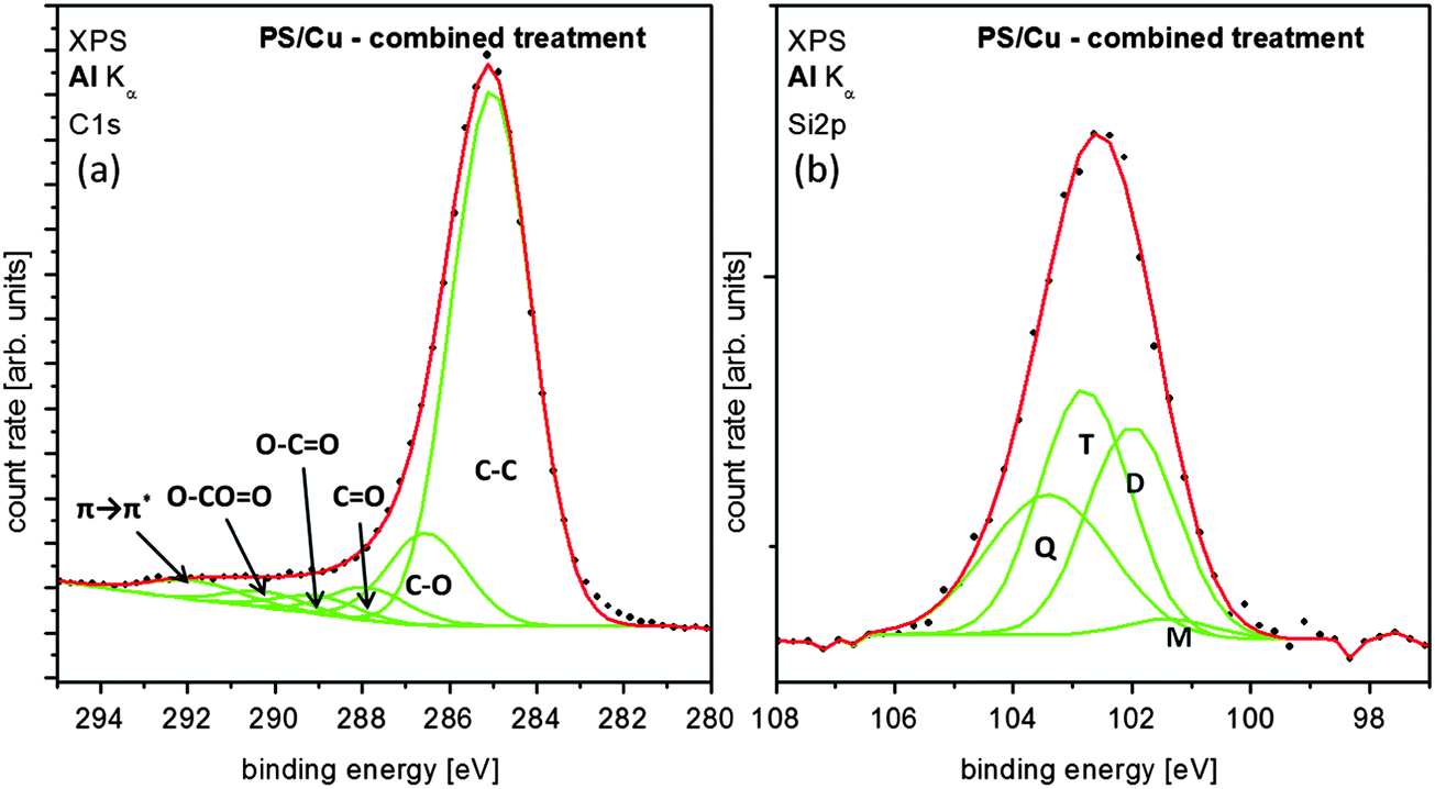 | ||
| Fig. 7 XPS detail spectra of the C 1s (a) and the Si 2p (b) regions after the combined functionalization. The components corresponding to different siloxy units are labelled M [(CH3)3SiO1/2], D [(CH3)2SiO2/2], T [(CH3)SiO3/2] and Q [SiO4/2] respectively.39 | ||
It is assumed that the aforementioned overlayer consists of polysiloxanes as related chemical treatments lead to such coatings.38 Therefore four components are assigned in the silicon peak in Fig. 7(b) that can be attributed to different siloxane units: M [(CH3)3SiO1/2] at 101.4 eV, D [(CH3)2SiO2/2] at 102.0 eV, T [(CH3)SiO3/2] at 102.8 eV and Q [SiO4/2] at 103.4 eV respectively.39 The chemical shifts of the components are taken from the literature.39–42 Even though the limited resolution of the spectrometer prohibits an absolutely assured assignment of the species, the decrease of the oxygen content as well as the increased amount of aliphatic carbon strongly support the polysiloxane approach of O'Hare et al. While there is only a small amount of M visible, the film mainly consists of the higher bound siloxane units D, T and Q. These results indicate that the chemical treatment of the template with DMDCS results in a protecting polysiloxane layer without disturbing the arrangement of the polystyrene spheres. The percent values may vary in the single-digit regime. They are obtained from the mathematical fit of the Si 2p spectrum shown in Fig. 7(b), which is based on FHWM and binding energy values taken from literature.39–42
The electrochemical deposition of materials in the interstices of colloidal crystals can disturb the order of the template, as mentioned above. This effect has been reported for lithium17 as well as for aluminum.15Fig. 8(a) depicts a SEM image of a colloidal crystal, which has been exposed to an oxygen DBD for 60 s prior to electrochemical deposition of copper. In the last step the polystyrene colloids are removed by THF. The image exhibits randomly distributed dark spots and brighter areas between them. The dark spots are holes or pores at the former positions of colloids, which have been removed by THF. The brighter areas between the pores consist of electrochemically deposited copper.
 | ||
| Fig. 8 SEM image of a polystyrene template subsequent to an oxygen plasma treatment, electrochemical deposition of copper and dissolution of the spheres in THF (a). SEM image of a template after an oxygen plasma treatment and polysiloxane protection (b), in which Cu was deposited. | ||
Two conclusions can be drawn from this experiment. First, as it is the case for lithium and aluminum, the process of depositing copper electrochemically in the colloidal crystal disorders the polystyrene colloids. The former fcc structure is not observed after copper deposition. Second, the preparation of the colloidal crystal by a DBD in oxygen alone does not stabilize the crystal structure for electrochemical deposition.
Fig. 8(b) shows a SEM image of a colloidal crystal acquired subsequent to the preparation by an oxygen DBD, the formation of a polysiloxane coating and electrochemical deposition of copper. Contrary to the sample in Fig. 8(a), the fcc order of the colloidal crystal is preserved due to the polysiloxane coating. The polystyrene spheres in the SEM image are intact and seem to be unaffected by electrochemical deposition. It is important to mention that the modified spheres are not dissolved by THF. This can be attributed to the chemical stability of the polysiloxane layer. The areas between the ordered spheres of the top layer are partly filled by a deposited material, Fig. 8(b). However the electrochemical data shows that copper has been deposited. The area marked with (1) in Fig. 8(b) shows a crack in the colloidal crystal, the underlying layer can be seen, furthermore the crack is not filled with a deposit. In area (2) a point defect due to a missing sphere is visible, with a deposit underneath.
Fig. 9 depicts a XPS survey spectrum recorded after the electrochemical deposition. Silicon is still visible in the spectrum, which indicates that the polysiloxane layer is intact, furthermore copper is now detected. Based on the experiments shown in Fig. 8 and and on the fact that electrochemical growth always starts at a conducting substrate, the interstices of the colloidal crystal must be filled with copper, which is supported by Fig. 9.
 | ||
| Fig. 9 XPS survey spectrum of polystyrene spheres after the functionalization by DBD, the coating with polysiloxane and the electrochemical deposition. | ||
These results imply the following:
• Dielectric barrier discharges in oxygen are an appropriate tool to functionalize the surface of polystyrene spheres for a subsequent coverage by a polysiloxane layer.
• The polysiloxane coating survived the electrochemical process and is thereby suitable to protect and stabilize templates of polystyrene spheres.
• Metals (here: copper) can be electrochemically deposited without disturbing the fcc arrangement of the spheres after polysiloxane coating.
4. Conclusion
Multilayer samples of hexagonally ordered polystyrene spheres were successfully prepared by dip coating. Afterwards the surface of the spheres has been activated in an oxygen DBD. During this process, oxygen-containing functional groups are formed at the surface in favor of aliphatic and aromatic bound carbon as verified by XPS. Subsequent coating of the spheres with polysiloxanes is accomplished in a chemical procedure, resulting in a protective, stabilizing layer covering the spheres for further use as a template. During the following electrochemical deposition of copper the polysiloxane coating persists, protecting the susceptible polystyrene surface below. The electrodeposition of Cu obviously does not alter the integrity of the modified PS template, thus the face centered cubic ordering of the template is preserved.In our opinion the proposed method to stabilize polystyrene spheres opens interesting opportunities to make stable 3-dimensional composite materials, e.g. for microbatteries or for photonic crystals.
Acknowledgements
We thankfully acknowledge the provision of the AFM by Prof. W. Daum. We thank Prof. W. Viöl for the support with the DBD and Silvia Löffelholz for the SEM measurements.References
- S. A. Asher, V. L. Alexeev, A. V. Goponenko, A. C. Sharma, I. K. Lednev, C. S. Wilcox and D. N. Finegold, J. Am. Chem. Soc., 2003, 125, 3322–3329 CrossRef CAS PubMed.
- J. H. Holtz and S. A. Asher, Nature, 1997, 389, 829–832 CrossRef CAS PubMed.
- W.-S. Chae, D. van Gough, S.-K. Ham, D. B. Robinson and P. V. Braun, ACS Appl. Mater. Interfaces, 2012, 4, 3973–3979 CAS.
- S. H. Park and Y. Xia, Langmuir, 1999, 15, 266–273 CrossRef CAS.
- Y. Xia, B. Gates, Y. Yin and Y. Lu, Adv. Mater., 2000, 12, 693–713 CrossRef CAS.
- K. Nagayama, Colloids Surf., A, 1996, 109, 363–374 CrossRef CAS.
- H. Cong, B. Yu, J. Tang, Z. Li and X. Liu, Chem. Soc. Rev., 2013, 42, 7774–7800 RSC.
- P. N. Bartlett, J. J. Baumberg, P. R. Birkin, M. A. Ghanem and M. C. Netti, Chem. Mater., 2002, 14, 2199–2208 CrossRef CAS.
- F. Endres, ChemPhysChem, 2002, 3, 144–154 CrossRef CAS.
- P. N. Bartlett, P. R. Birkin and M. A. Ghanem, Chem. Commun., 2000, 1671–1672 RSC.
- M.-C. Tsai, D.-X. Zhuang and P.-Y. Chen, Electrochim. Acta, 2010, 55, 1019–1027 CrossRef CAS PubMed.
- L. Ding, W. Yuren, M. Wenjie, C. He, X. Taohua and Y. Can, Appl. Surf. Sci., 2008, 254, 6775–6778 CrossRef PubMed.
- P. N. Bartlett, M. A. Ghanem, I. S. El Hallag, P. de Groot and A. Zhukov, J. Mater. Chem., 2003, 13, 2596–2602 RSC.
- F. Liu, Q. Yan, W. J. Zhou, X. S. Zhao and J. Y. Lee, Chem. Mater., 2006, 18, 4328–4335 CrossRef CAS.
- L. Gasparotto, A. Prowald, N. Borisenko, S. Z. El Abedin, A. Garsuch and F. Endres, J. Power Sources, 2011, 196, 2879–2883 CrossRef CAS PubMed.
- B. H. Juárez, C. López and C. Alonso, J. Phys. Chem. B, 2004, 108, 16708–16712 CrossRef.
- A. Willert, A. Prowald, S. Z. El Abedin, O. Höfft and F. Endres, Aust. J. Chem., 2012, 65, 1507–1512 CrossRef CAS.
- (a) B. J. Radola, Electrophoresis, 1980, 1, 43–56 CrossRef CAS; (b) A. Dawidowicz, A. Waksmundzki and S. Sokołowski, Sep. Sci., 1977, 12, 573–586 Search PubMed.
- F. Endres, MRS Bull., 2013, 38, 567–571 CrossRef CAS.
- J. Wen, Y. Yu and C. Chen, Mater. Express, 2012, 2, 197–212 CrossRef CAS PubMed.
- (a) P. Ferrand, M. J. Minty, M. Egen, J. Ahopelto, R. Zentel, S. G. Romanov and C. M. S. Torres, Nanotechnology, 2003, 14, 323–326 CrossRef CAS; (b) B. Lange, F. Fleischhaker and R. Zentel, Phys. Status Solidi A, 2007, 204, 3618–3635 CrossRef CAS; (c) P. Jiang, J. F. Bertone, K. S. Hwang and V. L. Colvin, Chem. Mater., 1999, 11, 2132–2140 CrossRef CAS.
- (a) U. Kogelschatz, Plasma Chem. Plasma Process., 2003, 23, 1–46 CrossRef CAS; (b) H. E. Wagner, R. Brandenburg, K. V. Kozlov, A. Sonnenfeld, P. Michel and J. F. Behnke, Vacuum, 2003, 71, 417–436 CrossRef CAS; (c) A. Fridman, A. Chirokov and A. Gutsol, J. Phys. D: Appl. Phys., 2005, 38, R1–R24 CrossRef CAS.
- L. Wegewitz, S. Dahle, O. Höfft, F. Voigts, W. Viöl, F. Endres and W. Maus-Friedrichs, J. Appl. Phys., 2011, 110, 33302 CrossRef PubMed.
- VSW Scientific Instruments, Instruction Manual HA Series Hemispherical Analysers. Techn. Ber., 1987.
- J. H. Scofield, J. Electron. Spectrosc. Relat. Phenom., 1976, 8, 129–137 CrossRef CAS.
- J. J. Yeh and I. Lindau, At. Data Nucl. Data Tables, 1985, 32, 1–155 CrossRef CAS.
- C. J. Powell and A. Jablonski, NIST Electron Inelastic-Mean-Free-Path Database. Version 1.2, National Institute of Standards and Technology, Gaithersburg, 2010 Search PubMed.
- R. Hesse, P. Streubel and R. Szargan, Surf. Interface Anal., 2005, 37, 589–607 CrossRef CAS.
- F. Marlow, M. Muldarisnur, P. Sharifi, R. Brinkmann and C. Mendive, Angew. Chem., Int. Ed., 2009, 48, 6212–6233 CrossRef CAS PubMed.
- M. Müller, R. Zentel, T. Maka, S. G. Romanov and C. M. Torres, Adv. Mater., 2000, 12, 1499–1503 CrossRef.
- D. Gogel, M. Weinl, J. K. N. Lindner and B. Stritzker, J. Optoelectron. Adv. Mater., 2010, 12, 740–744 CAS.
- A. Plettl, F. Enderle, M. Saitner, A. Manzke, C. Pfahler, S. Wiedemann and P. Ziemann, Adv. Funct. Mater., 2009, 19, 3279–3284 CrossRef CAS.
- L. Yan, K. Wang, J. Wu and L. Ye, J. Phys. Chem. B, 2006, 110, 11241–11246 CrossRef CAS PubMed.
- R. W. Paynter and D. Roy-Guay, Plasma Processes Polym., 2007, 4, 406–413 CrossRef CAS.
- A. Vesel, Surf. Coat. Technol., 2010, 205, 490–497 CrossRef CAS PubMed.
- G. Beamson and D. Briggs, High resolution XPS of organic polymers. The Scienta ESCA300 database, Wiley, Chichester, 1992 Search PubMed.
- (a) R. W. Paynter, Surf. Interface Anal., 1998, 26, 674–681 CrossRef CAS; (b) F. M. Petrat, D. Wolany, B. C. Schwede, L. Wiedmann and A. Benninghoven, Surf. Interface Anal., 1994, 21, 402–406 CrossRef CAS.
- A. Montarsolo, M. Periolatto, M. Zerbola, R. Mossotti and F. Ferrero, Text. Res. J., 2013, 83, 1190–1200 Search PubMed.
- L.-A. O'Hare, B. Parbhoo and S. R. Leadley, Surf. Interface Anal., 2004, 36, 1427–1434 CrossRef.
- L.-A. O'Hare, A. Hynes and M. R. Alexander, Surf. Interface Anal., 2007, 39, 926–936 CrossRef.
- J. Petersen, R. Bechara, J. Bardon, T. Fouquet, F. Ziarelli, L. Daheron, V. Ball, V. Toniazzo, M. Michel, A. Dinia and D. Ruch, Plasma Processes Polym., 2011, 8, 895–903 CrossRef CAS.
- D. S. Wavhal, J. Zhang, M. L. Steen and E. R. Fisher, Plasma Processes Polym., 2006, 3, 276–287 CrossRef CAS.
| This journal is © the Owner Societies 2014 |