CdS nanorod arrays with TiO2 nano-coating for improved photostability and photocatalytic activity
Liangpeng
Wu
a,
Yulan
Zhang
a,
Xinjun
Li
*a and
Chaoping
Cen
*b
aGuangzhou Institute of Energy Conversion, Chinese Academy of Sciences, Guangzhou 510640, China. E-mail: lixj@ms.giec.ac.cn; Fax: +86 2087057677; Tel: +86 20 87057781
bSouth China Institute of Environmental Science, Ministry of Environmental Protection, Guangzhou 510640, China. E-mail: cenchaoping@scies.org; Fax: +86 0285524451; Tel: +86 2085525914
First published on 29th May 2014
Abstract
CdS nanorod arrays were grown on fluorine-doped tin oxide glass substrates via a hydrothermal process and subsequently coated with a TiO2 nanolayer via a vacuum dip-coating process to fabricate a one-dimensional array structured photocatalyst. The TiO2 nanolayer improved the photocatalytic efficiency of CdS nanorod arrays for the degradation of methylene blue due to the effective separation of the electron–hole pairs, and the photocorrosion of CdS nanorod arrays was successfully inhibited.
Introduction
Since the identification of carbon nanotubes in 1991,1 one-dimensional (1D) nanostructures such as nanowires, nanobelts, nanoribbons, nanosheets, nanotubes and nanorods have attracted tremendous attention due to their unique electrical, optical and mechanical properties.2 Moreover, these nanostructures have potential application in the next-generation nanoscale electronics,3 functional materials,4,5 chemical sensors6 and optoelectronics.7 Particularly, 1D semiconductor arrays are considered as effective candidates for photoelectric and photochemical conversion owing to their large surface area, enhanced light absorption and reduced reflection, improved photogenerated carriers separation and collection, and the short path lengths for electrons and holes.8As an important and classical II–VI semiconductor, cadmium sulfide (CdS) with a direct band gap of 2.4 eV has been known to be one of the most fascinating semiconductor materials due to its various versatile properties such as a relatively low work function, excellent transport properties, unique photocatalytic activities and strong visible-light absorption as well as high electronic mobility.9 It has been extensively applied for degradation of pollutants, photocatalytic reduction of CO2 to solar fuel and hydrogen production in photoelectrochemical cells (PECs).10–14 Its photocatalytic activity has been found to be influenced by a variety of factors including particle size, morphology and crystallinity.15 For example, features such as good crystallinity, large surface area and morphology have been found to favor higher photocatalytic activity.16 It is noted that 1D CdS nanoarray structure can provide direct electron pathways for the photo-generated electrons to rapidly collect and transport, which will consequently enhance the photoelectrochemical performance of the photoelectrode. 1D CdS nanorod arrays (CdNRA) have been fabricated by chemical vapor deposition,17 solvothermal reaction,18 hydrothermal reaction19 and electrochemical synthesis.20 Li et al. studied the role of glutathione in shape control and the photoelectrical properties of CdSNRs, and further assembled hybrid solar cells with the configuration of FTO/CdS NRs/P3HT/Au. The performance of the FTO/CdS NRs/P3HT/Au hybrid was enhanced upon increasing the length of the as-prepared CdS nanorods.21,22 Chen's group reported the large-scale fabrication of CdS nanorod arrays on a transparent conductive tin-doped In2O3 (ITO) glass substrate by combining electrodeposition and hydrothermal processes.23 Sun et al. fabricated the oriented and high-density CdS nanorod arrays by facile chemical bath deposition, and demonstrated that the CdS nanorod arrays showed superior photoelectrochemical properties when the chemical bath deposition and hydrothermal time reached 0.5 h and 14 h, respectively.24 Guo et al. prepared CdS–CdSe core–shell nanorod arrays by chemical bath deposition. CdS–CdSe core–shell arrays gave a maximum photocurrent of 5.3 mA cm−2, which was 4 and 11 times as large as bare CdS and CdSe, respectively.25
CdS exhibits excellent photocatalytic activity because it shows highly effective absorption of solar energy.26,27 However, the oxidation of the sulfide ion by photogenerated holes is an intrinsic drawback for CdS-based photocatalysts. The photocorrosion problem makes CdS very unstable as a photocatalyst and greatly obstructs its practical application.28,29 In recent years, enormous efforts have been devoted to suppress the photocorrosion of CdS-based photocatalysts, such as combining CdS with another semiconductor,30 or embedding CdS particles in mesoporous materials31 or a polymer matrix to form hybrid photocatalysts,32 or using the sacrificial agents such as sulfide and/or sulfite salts.33 In addition, it is therefore absolutely vital to develop suitable surface engineering methods to inhibit the toxicity of leached Cd2+ ions. Coating CdS with a thin layer such as amorphous carbon, SiO2, TiO2, and ZnO may be an effective method to stabilize the surface and inhibit the photocorrosion process. Hu et al. reported a facile one-pot solvothermal method to synthesize carbon-coated CdS petalous nanostructures with uniform morphology. The resulting CdS–C hybrid particles exhibit excellent photostability and enhanced photocatalytic activity for the degradation of methyl orange and rhodamine B.34 Xu et al. synthesized 1D CdS@TiO2 core–shell nanocomposites via a two-step solvothermal method. An obvious enhancement of both conversion and yield is achieved over 1D CdS@TiO2 CSNs compared to bare CdS NWs, which is ascribed to the prolonged lifetime of photogenerated charge carriers over 1D CdS@TiO2 CSNs.35 Ouyang et al. fabricated a novel ZnO/CdS/TiO2 nanorod array composite structure, and found that the ZnO/CdS/TiO2 nanorod array film possesses stable and superior photoelectrocatalytic performance.36 Zhang et al. prepared the TiO2 nanotube array/CdS nanoparticles/ZnO nanorod photocatalyst, which exhibits higher removal ability for methyl and a high stability in photoelectrochemical oxidation.37
Herein, we report a facile and operable route to fabricate the CdSNRA@TiO2 composite photocatalyst. Ordered arrays of CdS nanorods are grown on fluorine-doped tin oxide (FTO) glass substrates by the hydrothermal method. And a TiO2 nanolayer is coated on CdSNRA via a vacuum dip-coating process. The photocatalytic activity under visible light irradiation was evaluated by photo-degradation of methylene blue (MB). The effect of the TiO2 nanolayer over CdSNRA on the improved photocatalytic activity and photostability was investigated (Scheme 1).
 | ||
| Scheme 1 Schematic diagram of the fabrication of the CdSNRA@TiO2 composite photocatalyst on FTO glass. | ||
Experimental
Preparation of CdSNRA and CdSNRA@TiO2
All chemicals were of analytical grade and used as received without any further purification.The ordered CdSNRA was prepared using the hydrothermal method, following the typical procedure.38 Firstly, FTO glasses were ultrasonically cleaned in acetone, isopropanol, ethanol and deionized (DI) water for 15 min each, respectively. Secondly, the mixture solution of cadmium nitrate, thiourea and glutathione with a molar ratio of 1![[thin space (1/6-em)]](https://www.rsc.org/images/entities/char_2009.gif) :1:0.4 (the concentration of cadmium nitrate is 48 mmol L−1) was added to a 100 mL Teflon-lined stainless-autoclave filled with 40 mL DI water after stirring under ambient conditions. After that, the cleaned FTO glasses were placed vertically at the bottom of the solution. The hydrothermal synthesis was conducted at 200 °C for 4.5 h in an electric oven. After synthesis, the reaction solution was cooled to room temperature naturally. Finally, the as-prepared sample was washed with DI water and dried naturally.
:1:0.4 (the concentration of cadmium nitrate is 48 mmol L−1) was added to a 100 mL Teflon-lined stainless-autoclave filled with 40 mL DI water after stirring under ambient conditions. After that, the cleaned FTO glasses were placed vertically at the bottom of the solution. The hydrothermal synthesis was conducted at 200 °C for 4.5 h in an electric oven. After synthesis, the reaction solution was cooled to room temperature naturally. Finally, the as-prepared sample was washed with DI water and dried naturally.
The TiO2 film layer on CdSNRA was prepared using the vacuum dip-coating process. Precursor solutions for the TiO2 thin layer were prepared according to the process reported in our previous work.39 Briefly, 68 mL of tetrabutyltitanate and 16.5 mL of diethanolamine were dissolved in 210 mL of absolute ethanol, and then the mixture was stirred vigorously for 1 h at room temperature (solution A). A mixture of 3.6 mL H2O and 100 mL ethanol (solution B) was added dropwise into the solution A under stirring. The resulting solution, an alkoxide solution, aged for 24 h at room temperature will result in a TiO2 sol. Under vacuum conditions, the substrate of CdSNRA was immersed into the TiO2 sol and withdrawn at the speed of 2 mm s−1. And then the samples were dried at 100 °C for 20 min. Finally, the samples were heat-treated at 450 °C for 30 min in an N2 atmosphere.
Characterization
The morphology of the samples was observed using a field emission scanning electron microscope (FESEM, HitachiS-4800) equipped with a detector for energy dispersive spectroscopy (EDS). The crystalline phases of the samples were investigated by X-ray diffraction (XRD, X' Pert-PRO, PANalytical, Holland) using Cu Kα radiation (λ = 0.154056 nm) at an accelerating voltage of 40 kV and a current of 40 mA. The patterns were recorded in the 2θ range from 10° to 80° at a scan rate of 1.5° min−1. Raman spectroscopy was carried out on LabRAM HR800 (ORIBAJY) equipment using a charged coupled device detector and a Leica DMLM microscope. The excitation source was a 532 nm laser beam. The absorption spectrum was recorded using a UV-visible spectrophotometer (LAMBDA 750) equipped with an integrating sphere and with BaSO4 as a reference in the range of 350–700 nm. The width of slit was 2.0 nm and the step was 0.5 nm.Photoeletrochemical measurements
Photoelectrochemical measurements were carried out in a three-electrode photoelectrochemical cell with a quartz window under the illumination of a 300 W Xe lamp (with a visible band pass filter glass, 420–770 nm) at room temperature. Transient photocurrent (iph) was measured using a CHI660A workstation (CHI Co.) in a standard three-electrode configuration with the as-prepared CdSNRA, CdSNRA@TiO2 as the photoanode, a Pt electrode as the counter electrode, and a saturated calomel electrode (SCE) as the reference electrode. 0.10 M Na2SO4 solution was chosen as the supporting electrolyte throughout the experiments for visible-light illumination.The photocatalytic activity was evaluated through the photocatalytic degradation of MB in the three electrode system with an area of 5 cm2 exposed to a quartz window for visible-light illumination. The volume of the reactor was 30 mL, where the initial concentration of MB was 5 × 10⁻⁶ M. The MB solutions were taken out to collect their UV-vis absorbance data once every 10 min.
Results and discussion
The crystallographic structure and phase purity of the samples were examined by X-ray diffraction (XRD) with the diffraction angle 2θ ranging from 10° to 80°. XRD patterns of CdSNRA and CdSNRA@TiO2 grown on a FTO substrate are shown in Fig. 1. The prepared CdSNRA and CdSNRA@TiO2 exhibit similar diffraction peaks. The characteristic peaks at 2θ values of 24.8°, 26.5°, 28.2°, 36.6°, 43.7°, 47.9°, 51.8°, 66.8° and 75.4° can be attributed to the (100), (002), (101), (102), (110), (103), (112), (203) and (105) crystal planes of CdS, respectively.35 According to the standard card (JCPDS #41-1049), all the diffraction peaks of CdSNRA can be assigned to the hexagonal structure. No characteristic peaks ascribed to other phases were observed, which indicates the high purity of the as-prepared CdSNRA. Furthermore, CdSNRA exhibits a much stronger reflection in the (002) direction as revealed by the XRD patterns, which suggests that CdSNRA grows preferentially oriented along the c-axis. The characteristic diffraction peaks of TiO2 could not be observed from the pattern of CdSNRA@TiO2. This might be attributed to its relatively low diffraction intensity. Besides, the primary characteristic peak of TiO2 at 2θ values of 25.4° might be overlapped with the (100) peak of hexagonal structure CdS. Nevertheless, due to the low loading of TiO2, the XRD pattern of TiO2 cannot be detected. However, Raman spectroscopy can confirm the presence of the TiO2 nanolayer on the surface of CdSNRA.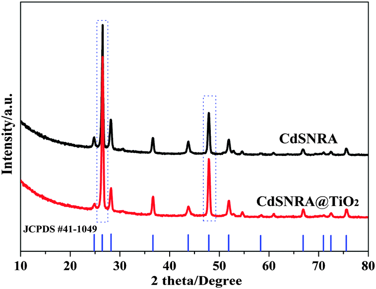 | ||
| Fig. 1 XRD patterns of CdSNRA and CdSNRA@TiO2. | ||
Raman scattering is a valuable spectroscopic technique that can be used to probe the electronic structure of semiconductors due to the strong electron–phonon interaction in solid, liquid or gas samples. Raman spectra of CdSNRA@TiO2 and CdSNRA are displayed in Fig. 2. The Raman spectrum of CdSNRA is dominated by an intense band at 300 cm−1, assigned to the first-order longitudinal optic phonon (1 LO) and the second-order LO phonon peak at 600 cm−1.40 In comparison to the spectrum of CdSNRA, the additional peaks at 149 cm−1 and 516 cm−1 are found in the spectrum of CdSNRA@TiO2.41 The two peaks are assigned to the surface optical phonons vibration mode of anatase TiO2, which confirm the formation of TiO2 on the surface of CdSNRA.42
 | ||
| Fig. 2 Raman spectra of CdSNRA and CdSNRA@TiO2. Laser excitation wavelength at 532 nm. | ||
The FESEM image of CdSNRA is shown in Fig. 3a. The image reveals that CdSNRA, which has a uniform morphology and is hexagonal, could be observed on FTO glass. The length of CdSNRA is about 300–400 nm by observing the cross-sectional SEM image of CdSNRA grown on FTO glass (see Fig. 3a). Meanwhile, we could see that a compact layer of CdS nanoparticles is deposited on FTO glass. It is suggested that the formation process of CdSNRA could be divided into two steps. In the beginning, CdS nanoparticles are selectively deposited on the FTO substrate. Then CdSNRA grows on those nanoparticles. The result corresponded well with the previous report.38 The FESEM image of CdSNRA@TiO2 on the FTO substrate is shown in Fig. 3b. The diameter of the rods is increased, and the rods get more roughness after coating the TiO2 nanolayer on CdSNRA. Fig. 3c shows a cross-sectional SEM image of CdSNRA@TiO2 on FTO substrates in which a thin TiO2 shell covers the surface of CdSNRA. Energy-dispersive X-ray spectroscopy (EDX) analysis is carried out to identify the elemental composition of CdSNRA@TiO2, and the EDX spectrum is shown in Fig. 3d. The Mα peak of Cd and S can be clearly seen at 2.8 and 2.35 keV, respectively. A moderate Kα peak of the element O can also be observed at 0.52 keV. A moderate Kα peak of the element Ti can be observed at 0.4, 4.65, and 4.95 keV.43 In order to verify the layer nanoarray structure of CdSNRA@TiO2, the electron mapping image analysis of the sample is recorded and shown in Fig. 3e–h. The above edge region clearly shows cylindrical shell contrast reflecting the layers, and the EDS elemental mapping confirmed localized Cd and S in the filled core area. And the elemental mapping of Ti and O in Fig. 3g and h demonstrates the presence of the TiO2 shell on the surface of CdSNRA.
 | ||
| Fig. 3 SEM images of CdSNRA (a), CdSNRA@TiO2 (b), the cross-section SEM image (c) and EDS spectrum (d) of the CdSNRA@TiO2 edge region, and the corresponding EDS elemental mapping of Cd, S, Ti and O (e–h). | ||
The UV-vis diffuse reflectance spectra are used to determine the optical properties of the samples. The absorption properties of CdSNRA and CdSNRA@TiO2 are shown in Fig. 4. Coating the TiO2 nanolayer onto CdSNRA has a significant effect on the optical properties in the ultraviolet (UV) region. It is clear that CdSNRA@TiO2 exhibits enhanced light absorption capacity in the UV region, compared to CdSNRA. This is understandable because TiO2 has a UV light response. And the absorption edge of CdSNRA appeared at about 560 nm corresponding to the band gap value of 2.24 eV. Compared with CdSNRA, the TiO2 nanolayer coated on CdSNRA shows the enhanced visible-light absorption at the sub-band gap range.
 | ||
| Fig. 4 Diffuse reflectance UV-vis spectra of CdSNRA and CdSNRA@TiO2. | ||
The photoluminescence (PL) technique is an effective way to investigate the efficiency of the charge carrier trapping, migration, and transfer due to the PL signals of semiconductor materials, resulting from the recombination of photo-induced charge carriers. The typical PL spectra of CdSNRA and CdSNRA@TiO2 are measured with the excitation wavelength of 532 nm as shown in Fig. 5. It is observed that the PL intensity of the broad peak is changed between 500 and 650 nm corresponding to the two distinct green emission ranges at ∼528 and 590 nm, which is consistent with the previous reports.44 The former one can be assigned to near-band-edge emission, and the latter is associated with structural defects that may arise from the excess of sulfur or core defects on the surfaces.45 As displayed in Fig. 5, the PL intensities of the CdSNRA@TiO2 sample are much weaker than that of the pure CdSNRA sample, thus suggesting a longer lifetime of photo-generated charge carriers from 1D CdSNRA@TiO2. This is due to the reduced surface states at grain boundaries which act as luminescence sequesters.46 It is therefore concluded that the TiO2 nanolayer on the CdSNRA surface effectively passivates the CdS surface, inhibits the charge carrier recombination, prolongs the lifetime of the charge carriers and protects the CdSNRA from photocorrosion. The charge carriers with prolonged lifetime photoinduced from 1D CdSNRA@TiO2 are beneficial for the improved photocatalytic activity and photostability.
 | ||
| Fig. 5 Photoluminescence spectra of the bare CdSNRA and CdSNRA@TiO2 at room temperature with a 532 nm excitation wavelength. | ||
To test the photoelectrochemical response of as-prepared photoelectrodes under visible light irradiation, transient photocurrent was measured. iph is generated from the excited photoelectrons from the valence band to the conduction band and mainly reflects the conductance value and the number of free photogenerated carriers in the semiconductor. The photocurrent responses of CdSNRA and CdSNRA@TiO2 in 0.10 M Na2SO4 solution are measured in the light on–off process with a pulse of 10 s using the potentiostatic technique under visible light irradiation and shown in Fig. 6. The current responses in the dark were negligible. In the case of visible light illumination, an apparently boosted photocurrent response appeared, indicating photoelectrocatalysis. At the preliminary stage of illustration, the iph of the CdSNRA electrode is larger than that of the CdSNRA@TiO2 photoelectrode. Subsequently, the iph of the CdSNRA photoelectrode decays gradually with the increase of the on–off cycles illustration. At the later stage of illustration, it is even lower than that of the CdSNRA@TiO2 photoelectrode. This result indicated that the TiO2 nanolayer could serve as a shell reducing the recombination of electron–hole pairs and enhancing the transfer of charge carriers, further protecting CdSNRA from photocorrosion. Similarly to the EIS results, the CdSNRA@TiO2 electrode shows a lower recombination rate of photo-induced electron–hole pairs than the pure CdSNRA electrode, according to the smaller radius of the arc on the EIS Nyquist plot in Fig. 7a. This indicates that the TiO2 nanolayer coated on the CdSNRA surface gives rise to a good interaction resulting in an efficient and faster charge transfer. Meanwhile, the characteristic frequency peaks of CdSNRA and CdSNRA@TiO2 in Bode phase plots, which can be related as the inverse of the recombination lifetime (τr) or electron lifetime (τe), are shown in Fig. 7b. The characteristic frequency peak shifted to lower frequency in the presence of the TiO2 nanolayer. This further indicates that the TiO2 nanolayer could reduce the electron recombination and extend the electron lifetime.
 | ||
| Fig. 6 Transient photocurrents of CdSNRA and CdSNRA@TiO2. | ||
 | ||
| Fig. 7 EIS results of pure CdSNRA and CdSNRA@TiO2 photoelectrodes under visible light irradiation: (a) Nyquist plots; (b) Bode phase plots. | ||
Compared with the photocatalytic activity, the stability of the photocatalyst properties related to applications is much more important. In other words, a number of efforts must be made to prohibit the deactivation of the photocatalyst for better sustainable reuse. Therefore, the photocatalytic test on the reusability of CdSNRA@TiO2 is necessary. The photocatalytic activity of CdSNRA and CdSNRA@TiO2 was evaluated for the degradation of MB under visible-light irradiation. The MB degradation ratio for the CdSNRA@TiO2 photoelectrode was slightly larger than that of the CdSNRA photoelectrode under visible light irradiation. To test the repeatability of MB degradation by the samples of CdSNRA and CdSNRA@TiO2 photoelectrodes, a degradation experiment was carried out and repeated three times under visible light irradiation. The experimental results are shown in Fig. 8. The photocatalytic activity of CdSNRA decreases in the third run. However, there is no remarkable difference between the three repeated batches for CdSNRA@TiO2 photocatalytic degradation of MB. The photocurrent testing results could also support this conclusion. After the photocatalytic degradation of MB for three recycles reaction, the hexangularly faced and smooth surface topography of CdSNRA can hardly be seen and only multiporous morphologies exist as shown in Fig. 9a, which indicates that the CdSNRA structure has changed. However, in the presence of the TiO2 nanolayer, the morphology of CdSNRA is retained as shown in Fig. 9b. In addition, the corresponding XRD patterns of CdSNRA and CdSNRA@TiO2 after photocatalytic degradation of MB are also shown in Fig. 9c. The XRD patterns of CdSNRA@TiO2 showed no notable differences. However, the diffraction peak intensity of CdSNRA decreased after photocatalytic degradation of MB, and the diffraction peak of S appeared. These results indicate that the CdSNRA photocatalyst was not stable and photocorrosion occurred during the reaction. The CdSNRA@TiO2 photocatalyst was stable enough and the TiO2 nanolayer could protect CdSNRA from photocorrosion.
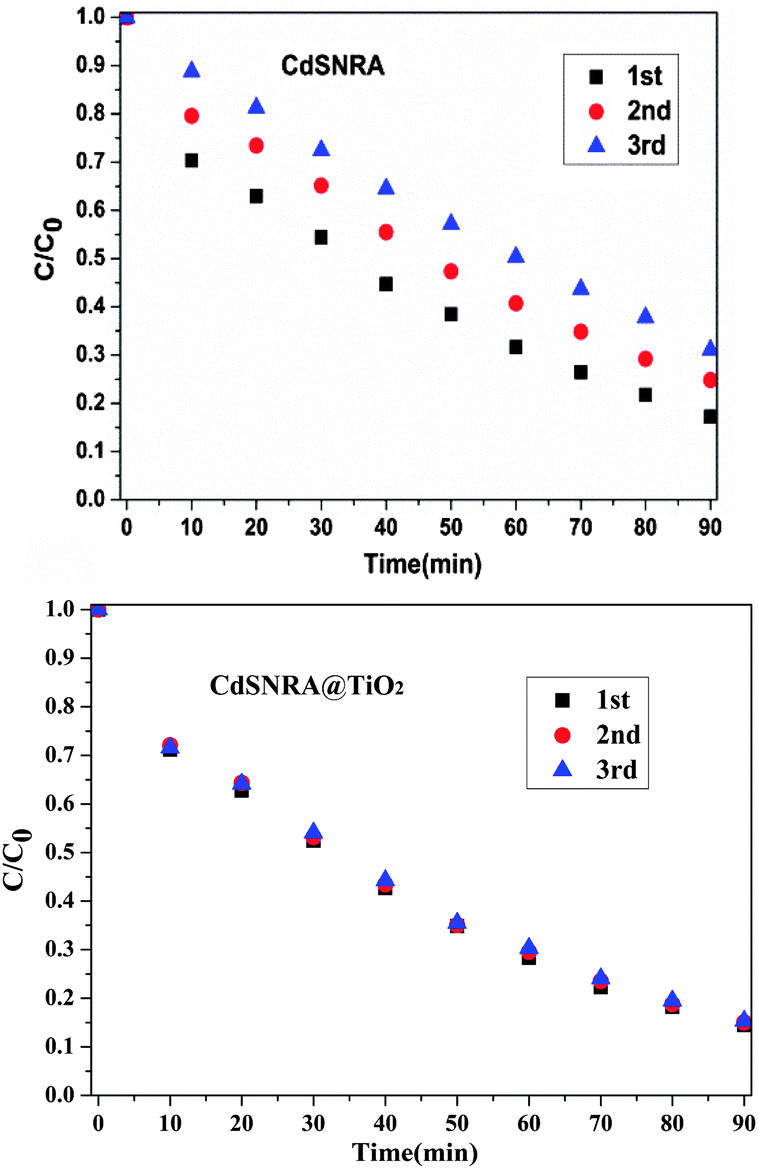 | ||
| Fig. 8 Photoelectrocatalysis degradation of MB over CdSNRA and CdSNRA@TiO2 photoelectrodes under visible light irradiation. | ||
 | ||
| Fig. 9 SEM images of CdSNRA (a) and CdSNRA@TiO2 (b), XRD patterns (c) after photocatalysis degradation of MB under visible-light irradiation. | ||
It has been established that CdS generally suffers from photocorrosion due to the oxidation of CdS by its own photogenerated holes, especially in aqueous solution. Based on the experimental results above, it could be concluded that the TiO2 nanolayer coated on the surface of CdSNRA exhibits better photocatalytic efficiency and photocatalytic stability than pure CdSNRA in the degradation of MB under visible light irradiation. A possible photocatalytic mechanism for the CdSNRA@TiO2 structure photocatalyst is proposed, as illustrated in Scheme 2. Under the illumination of visible light, the efficient two-level charge transfer from CdS to TiO2 occurs for photocatalytic reactions. The photogenerated electrons are excited from the valence band (VB) of CdSNRA to the conduction band (CB), forming the electron–hole pairs. The CB of TiO2 is less negative than the CB of CdS; therefore, the photoexcited electrons from the CB of CdS transfer to the CB of TiO2.35,42 Thus, the separation of photogenerated electron–hole pair is improved and the lifetime of the carriers is prolonged, indicating that the recombination of photogenerated electron–hole pairs is hampered in CdSNRA@TiO2. Subsequently, the photogenerated electrons could be propitious to transfer to the external circuit (Pt electrode), to form activated oxygen (e.g., O2˙−) by reacting with molecular oxygen and finally reduce directly the adsorbed H+ to H2O. Simultaneously, on account of the thin TiO2 shell, the photogenerated holes from CdSNRA are powerful enough to oxidize surface-adsorbed hydroxy groups and water molecules, which subsequently attack the organic compound and is responsible for the photocatalytic degradation of organic pollutants, such as MB.47 Meanwhile, due to the presence of the thin TiO2 nanolayer, more absorbance of visible light is achieved and the surface area is enhanced, thereby providing a sufficient opportunity for spatial contact between photocatalytic active species and reactants.48 What is important is that the thin TiO2 layer enwrapping CdSNRA could efficiently accept the electrons to boost the separation of the photogenerated electron–hole pairs, thus effectively prolonging the lifetime of the charge carriers and reducing the photodecomposition process of CdSNRA, causing increased stability of the CdSNRA@TiO2 photoelectrode.
 | ||
| Scheme 2 Illustration of the proposed reaction mechanism for selective oxidation of MB over the 1D CdSNRA@TiO2 under visible light irradiation. | ||
In addition, the 1D array structure photocatalyst allows for an oriented and much shorter random walk path for the photogenerated carriers to increase the charge-collection efficiency and improve electron lifetimes.46 Owing to the effective charge separation and longer lifetime of the electron–hole pairs, the separated electrons and holes participate in reduction (cathode) and oxidation (anode) reaction, respectively. The rate of hole–electron recombination in CdSNRA is suppressed. Thus, the light conversion efficiency and photoability are enhanced effectively. As a result of the TiO2 nanolayer protection, the photo-corrosion and/or oxidation of CdSNRA is successfully inhibited.
Conclusion
In summary, we report a facile and operable method to fabricate the 1D CdSNRA@TiO2 composite photocatalyst. Ordered arrays of CdS nanorods are grown on FTO glass substrates by the hydrothermal method. And the TiO2 nanolayer was coated on CdSNRA via a vacuum dip-coating process. The CdSNRA@TiO2 photocatalyst exhibits enhanced photocatalytic activity and photostability for degrading MB. This could be attributed to the TiO2 nanolayer that can effectively transfer the photogenerated hole to cause the effective charge separation and protect CdSNRA against photocorrosion.Acknowledgements
The work is supported by the Science & Technology Plan Project of Guangzhou City, China (No. 2013J4300035), the National Natural Science Foundation of China (No. 51172233) and the Foundation of the Key Laboratory of Water and Air Pollution Control of Guangdong Province (GD2012A05).Notes and references
- S. Iijima, Nature, 1991, 354, 56 CrossRef CAS.
- Y. S. Zhao, H. Fu, A. Peng, Y. Ma, Q. Liao and J. Yao, Acc. Chem. Res., 2010, 43, 409 CrossRef CAS PubMed.
- X. L. Li, Y. Jia and A. Y. Cao, ACS Nano, 2010, 4, 506 CrossRef CAS PubMed.
- Y. Cui and C. M. Lieber, Science, 2001, 291, 851–853 CrossRef CAS PubMed.
- N. Zhang, R. Ciriminna, M. Pagliaro and Y. J. Xu, Chem. Soc. Rev., 2014 10.1039/C4CS00056K.
- A. Ferancov, S. Rengaraj, Y. Kim, J. Labuda and M. Sillanp, Biosens. Bioelectron., 2010, 26, 314 CrossRef PubMed.
- Z. Li, L. Cheng, Q. Sun, Z. Zhu, M. J. Riley, M. Aljada, Z. Cheng, X. Wang, G. R. Hanson, S. Qiao, S. C. Smith and G. Q. Lu, Angew. Chem., Int. Ed., 2010, 49, 2777 CrossRef CAS PubMed.
- K. S. Leschkies, R. Divakar, J. Basu, E. Enache-Pommer, J. E. Boercker, C. B. Carter, U. R. Kortshagen, D. J. Norris and E. S. Aydil, Nano Lett., 2007, 7, 1793 CrossRef CAS PubMed.
- Y. F. Lin, J. Song, Y. Ding, S. Y. Lu and Z. L. Wang, Adv. Mater., 2008, 20, 3127 CrossRef CAS.
- N. Zhang, S. Q. Liu and Y. J. Xu, Nanoscale, 2012, 4, 2227 RSC.
- S. Q. Liu, M. Q. Yang and Y. J. Xu, J. Mater. Chem. A, 2014, 2, 430 CAS.
- J. G. Yu, J. Jin, B. Cheng and M. Jaroniec, J. Mater. Chem. A, 2014, 2, 3407 CAS.
- M. Q. Yang and Y. J. Xu, Phys. Chem. Chem. Phys., 2013, 15, 19102 RSC.
- J. Zhang, S. Z. Qiao, L. F. Qi and J. G. Yu, Phys. Chem. Chem. Phys., 2013, 15, 12088 RSC.
- X. B. Chen, S. H. Shen, L. J. Guo and S. S. Mao, Chem. Rev., 2010, 110, 6503 CrossRef CAS PubMed.
- N. Z. Bao, L. M. Shen, T. Takata, K. Domen, A. Gupta, K. Yanagisawa and C. A. Grimes, J. Phys. Chem. C, 2007, 111, 17527 CAS.
- T. Y. Zhai, X. S. Fang, Y. Bando, Q. Liao, X. J. Xu, H. B. Zeng, Y. Ma, J. N. Yao and D. Golberg, ACS Nano, 2009, 3, 949 CrossRef CAS PubMed.
- M. M. Zhou, S. C. Yan, Y. Shi, M. Yang, H. B. Sun, J. Y. Wang, Y. Yin and F. Gao, Appl. Surf. Sci., 2013, 273, 89 CrossRef CAS PubMed.
- B. L. Cao, Y. Jiang, C. Wang, W. H. Wang, L. Z. Wang, M. Niu, W. J. Zhang, Y. Q. Li and S. T. Lee, Adv. Funct. Mater., 2007, 17, 1501 CrossRef CAS.
- S. Higashimoto, K. Kawamoto, H. Hirai, M. Azuma, A. Ebrahimi, M. Matsuoka and M. Takahashi, Electrochem. Commun., 2012, 20, 36 CrossRef CAS PubMed.
- C. Y. Yang, S. Liu, M. R. Li, X. L. Wang, J. Zhu, R. F. Chong, D. Yang, W. H. Zhang and C. Li, J. Colloid Interface Sci., 2013, 393, 58 CrossRef CAS PubMed.
- C. Y. Yang, M. R. Li, W. H. Zhang and C. Li, Sol. Energy Mater. Sol. Cells, 2013, 115, 100 CrossRef CAS PubMed.
- X. X. Jiang, F. Chen, H. Xu, L. G. Yang, W. M. Qiu, M. M. Shi, M. Wang and H. Z. Chen, Sol. Energy Mater. Sol. Cells, 2010, 94, 338 CrossRef CAS PubMed.
- M. L. Sun, W. Y. Fu, Q. Li, G. C. Yin, K. L. Chi, X. M. Zhou, J. W. Ma, L. H. Yang, Y. N. Mu, Y. L. Chen and H. B. Yang, J. Cryst. Growth, 2013, 377, 112 CrossRef CAS PubMed.
- M. Wang, J. G. Jiang, J. W. Shi and L. J. Guo, ACS Appl. Mater. Interfaces, 2013, 5, 4021 CAS.
- L. P. Wu, Y. L. Zhang, L. Z. Long, C. P. Cen and X. J. Li, RSC Adv., 2014, 4, 20716 RSC.
- N. Zhang, Y. H. Zhang and Y. J. Xu, Nanoscale, 2012, 4, 5792 RSC.
- N. Zhang, M. Q. Yang, Z. R. Tang and Y. J. Xu, J. Catal., 2013, 303, 60 CrossRef CAS PubMed.
- A. Kudo and Y. Miseki, Chem. Soc. Rev., 2009, 38, 253 RSC.
- J. K. Jang, S. M. Ji, S. W. Bae, H. C. Son and J. S. Lee, J. Photochem. Photobiol., A, 2007, 188, 112 CrossRef CAS PubMed.
- S. Y. Ryu, W. Balcerski, T. K. Lee and M. R. Hoffmann, J. Phys. Chem. C, 2007, 111, 18195 CAS.
- J. Jang, S. H. Kim and K. J. Lee, Chem. Commun., 2007, 2689 RSC.
- X. W. Wang, G. Liu, Z. G. Chen and F. Li, J. Mater. Res., 2010, 25, 39 CrossRef CAS.
- Y. Hu, X. H. Gao, L. Yu, Y. R. Wang, J. Q. Ning, S. J. Xu and X. W. Lou, Angew. Chem., Int. Ed., 2013, 52, 5636 CrossRef CAS PubMed.
- S. Q. Liu, N. Zhang, Z. R. Tang and Y. J. Xu, ACS Appl. Mater. Interfaces, 2012, 4, 6378 CAS.
- J. L. Ouyang, M. L. Chang and X. J. Li, J. Mater. Sci., 2012, 47, 4187 CrossRef CAS.
- Y. N. Zhang, G. H. Zhao, Y. Z. Lei, P. Q. Li, M. F. Li, Y. N. Jin and B. Y. Lv, ChemPhysChem, 2010, 11, 3491 CrossRef CAS PubMed.
- F. Chen, R. J. Zhou, L. G. Yang, M. M. Shi, G. Wu, M. Wang and H. Z. Chen, J. Phys. Chem. C, 2008, 112, 13457 CAS.
- Y. Yang, X. J. Li, J. T. Chen and L. Y. Wang, J. Photochem. Photobiol., A, 2004, 163, 517 CrossRef CAS PubMed.
- B. Schreder, C. Dem, M. Schmitt, A. Materny, W. Kiefer, U. Winkler and E. Umbach, J. Raman Spectrosc., 2003, 34, 100 CrossRef CAS.
- A. Kontos, V. Likodimos, E. Vassalou, I. Kapogianni, Y. Raptis, C. Raptis and P. Falarasp, Nanoscale Res. Lett., 2011, 6, 1 CrossRef PubMed.
- Z. Chen and X. J. Xu, ACS Appl. Mater. Interfaces, 2013, 5, 13353 CAS.
- L. P. Wu, J. Li, S. H. Zhang, L. Z. Long, C. P. Cen and X. J. Li, J. Phys. Chem. C, 2013, 117, 22591 CAS.
- Y. Y. Xi, J. Z. Zhou, H. H. Guo, C. D. Cai and Z. H. Lin, Chem. Phys. Lett., 2005, 412, 60 CrossRef CAS PubMed.
- D. Xu, Z. Liu, J. Liang and Y. Qian, J. Phys. Chem. B, 2005, 109, 14344 CrossRef CAS PubMed.
- G. Q. Xu and B. Liu, J. Phys. Chem. Solids, 2000, 61, 829 CrossRef CAS.
- M. S. Suleymanov, Int. J. Hydrogen Energy, 1991, 16, 741 CrossRef.
- D. Kim, A. Ghicov, S. P. Albu and P. Schmuki, J. Am. Chem. Soc., 2008, 130, 16454 CrossRef CAS PubMed.
| This journal is © the Owner Societies 2014 |