
 Open Access Article
 This Open Access Article is licensed under a Creative Commons Attribution-Non Commercial 3.0 Unported Licence
Hydrogen-dimer lines and electron waveguides in graphene†
Simona
Achilli
ab,
Gian Franco
Tantardini
ab and
Rocco
Martinazzo
*ab
aDipartimento di Chimica, Università degli Studi di Milano, v. Golgi 19, 20133, Milano, Italy. E-mail: rocco.martinazzo@unimi.it; Fax: +39 02 50314300; Tel: +39 02 50314287
bIstituto di Scienze e Tecnologie Molecolari, Consiglio Nazionale delle Ricerche, Milano, Italy
First published on 27th June 2014
Abstract
The electronic and transport properties of graphene ribbons sandwiched between hydrogen dimer lines, of the kind recently realized by Nilsson et al., Carbon, 2012, 50, 2052, are investigated with the help of first principles methods. It is found that such lines of hydrogen atoms block conduction between neighboring channels and effectively allow the confinement of graphene charge carriers, thereby opening the possibility of imprinting nano-circuits in graphene by controlled hydrogenation.
1 Introduction
The isolation of graphene,1 the one-atom thick layer of carbon atoms arranged in a honeycomb lattice, opened new avenues for miniaturizing electronic devices, due to the combination of the highly flexible, mechanically stable structure of graphene and the extraordinary properties of its Dirac electrons.2–5 The remarkable possibility of tuning its electronic properties to a large extent upon nanostructuring makes it promising for various applications, and graphene-based devices may be superior to current technologies and help to facilitate new ones.Well-known examples of graphene nanostructures are graphene nanoribbons (GNRs)6,7 where, analogously to carbon nanotubes,8,9 electron confinement in the direction perpendicular to the ribbon axis opens a band-gap in their electronic structure and makes them suitable for logic applications, with potentially outstanding performances.10 Current limitations to the practical exploitation of GNRs arise from the lack of control over the edge geometry, though recent progress in controlled hydrogen etching is promising in this respect.11,12 Graphene nanoribbons with desired edges have indeed been produced by a chemical synthetic route on a metallic surface,13,14 and recently proved to be transferable onto an insulating substrate,15 but practical ways to realize bottom-up GNR transistors remain challenging to develop. Likewise if atomic-scale defects (e.g. carbon atom vacancies, voids and chemisorbed atoms) are introduced in the lattice: whether precise control of the defect positions was achieved, regularly arranged superlattice structures would display highly desirable properties – including a band-gap16,17 – thanks to the huge impact that such kinds of defects have on the low energy electronic structure of graphene.18–20
Recently, it has been predicted that parallel lines of chemisorbed hydrogen atoms split a graphene sheet into pseudo-ribbons with semimetal or semiconducting properties, similar to conventional nanoribbons.21–24 Analogues of armchair graphene nanoribbons (aGNRs) were conceived by placing lines of hydrogen atoms along an armchair direction in graphene, and were found to have a band-gap of a size similar to that of an aGNR with the same width.23 Electron waveguides that could act as two or three terminal junctions and serve as nano-diodes, nano-transistors or logic network units were also envisaged with lines of hydrogen atoms playing the role of confining walls.24 Along the same line of thought, Rasmussen et al.25 have recently shown how to stabilize single and multiple kinks in graphene by placing hydrogen lines along an armchair direction, thereby forming pseudo-ribbons with transport properties similar to those of conventional aGNRs. Similarly, Gunlycke et al.26 investigated chemical decoration of a common extended line defect (the 5-5-8 topological defect line), and showed that such nano-structuring creates confinement and resonance bands which trace the bands in zig-zag nanoribbons and display remarkable valley polarization properties. Importantly, in such approaches, defects (chemisorbed atoms) are used to imprint ribbons on graphene rather than cutting them out of it, thereby allowing the use of one and the same substrate as a support for integrated (nano)circuits.
In practice, the possibility of realizing the above structures by simply adsorbing hydrogen atoms on graphene is hampered by the unavoidable randomness of the adsorption process. Though well defined dimers (the so-called ortho- and para-dimers) do preferentially form when exposing graphene (graphite) to a hot hydrogen beam,27 the regioselectivity of the adsorption process strongly depends on the number and position of the already adsorbed species, as a consequence of the aromatic character of the substrate.28 As a result, a random distribution of dimers is usually found on the surface, which turns into clustering at high hydrogen doses,27,29 because the substrate softening accompanying hydrogenations causes a (local) enhancement of the reactivity of the surface. Eventually, disordered hydrogenated graphene is achieved, possibly with local graphane-like domains,30 and a metal–insulator transition is already triggered at a modest hydrogen coverage.31
Progress in controlling hydrogenation has been made by exploiting superlattice (Moiré) structures, which arise naturally when graphene grows on a crystalline substrate. Indeed, beside inducing superlattice potentials for graphene charge carriers,32 substrates may act as templates for patterned adsorption even when graphene binds only weakly to them. This is the case, for instance, for graphene on Ir(111) where hydrogenated structures were formed which followed the superlattice periodicity, and were shown to open a gap in the electronic band structure.33
More recently, it has been shown that pairs of hydrogen lines of the type mentioned above do indeed form on graphite upon hydrogen exposure if the surface is pre-covered with a self-assembled monolayer of cyanuric acid.34 Such structures were investigated by combining Scanning Tunneling Microscopy (STM) with Density Functional Theory (DFT) calculations and were found to be highly stable, thanks to the balanced mixture of ortho- and para-dimer configurations which naturally appears along an armchair direction. One specific pair of such hydrogen-dimer lines was identified by its STM image and appeared as bright lines enclosing a dark region, thereby suggesting a reduction of the conductivity between the defect lines.34
In view of the above, in this paper we study in detail the electronic and transport properties of the structures produced by Nilsson et al.34 and similar structures of different sizes. In particular, we investigate whether electronic confinement does indeed occur and how it affects electronic transport. To this end, we consider transport in a direction either parallel or perpendicular to the dimer lines (in the disorder-free ballistic regime where the geometry of the transport channels alone determines the conduction properties), and characterize its spatial features by means of transport eigenchannels. Our results confirm that hydrogen-dimer lines indeed act as impenetrable walls for graphene charge carriers and split the graphene sheet into independent transport channels that can be used for realizing nano-transistors and electron waveguides in graphene.
The paper is organized as follows. Section 2 gives some details concerning the chosen models and the adopted theoretical approach, Sections 3.1–3.4 describe, respectively, the electronic structure and the transport properties of the systems considered, and finally Section 4 summarizes and concludes.
2 Theory
2.1 Methods
Electronic structure and transport calculations were performed at the Density Functional Theory level, within the generalized gradient approximation, employing the Perdew–Burke–Ernzerhof functional35,36 to handle exchange and correlation effects. Core-electrons were described by separable norm-conserving pseudopotentials37 with a partial core correction,38 and a set of numerical atomic orbitals with compact support of double-ζ plus polarization quality was used to expand the wavefunction, as implemented in SIESTA.39 Brillouin zone (BZ) sampling was performed following the Monkhorst–Pack scheme40 with a few hundred independent k-points for each periodic direction, depending on the structure considered. Structural and transport calculations were artificially periodic in the direction perpendicular to the graphene plane, and a large vacuum layer (∼20 Å) was introduced to ensure negligible interaction between layers, along with a simple one-k point sampling of the BZ along this direction, as usual.Transport properties were computed with standard non-equilibrium Green's function (NEGF) techniques that use the corresponding Kohn–Sham one-electron Hamiltonian, HKS. In such a set-up three different regions are identified, two semi-infinite leads and a central scattering region. Transport properties require calculation of the retarded Green's function of the scattering region, upon proper inclusion of the electrodes self-energies in the scattering-region Hamiltonian. The latter are obtained separately by standard DFT periodic calculations for the semi-infinite electrodes alone, and the Hamiltonian (Green's function) is made self-consistent with the charge density it describes, for each applied bias, as implemented in TRANSIESTA.41
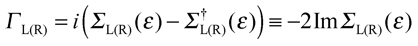
The zero-temperature, linear-regime conductance G is given (in units of quantum of conductance G0 = 2e2/h = 77.48 μS appropriate for spin-unpolarized channels) by the cumulative transmission probability N(ε)42
| N(ε) = Tr[G†(ε)ΓR(ε)G(ε)ΓL(ε)] |
 of the left (L) and right (R) electrodes. In practice, in the above expression Tr stands for an ordinary trace, and the operators G, Σ, etc., are understood to be their matrix representation in the chosen basis.
More generally, the current flowing from L to R follows from

Spatial features of conduction modes were analyzed with transmission (left) eigenchannels.43 These are eigenvectors of the product current operator in the device subspace of the left-incoming scattering states, and describe independent transport channels with transmission probabilities tm(ε) given by the corresponding eigenvalues 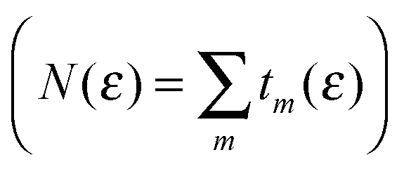 . They were computed with the above G(ε) and ΓL(R), as described in ref. 43 and 44, by means of INELASTICA.45
2.2 Structural models
Electronic structure was investigated in superlattices describing parallel hydrogen-dimer lines, i.e. structures where hydrogen atoms sit on every lattice position of parallel armchair directions in graphene. Generally speaking, two such lines may be superimposed by a lattice translation along one zig-zag direction, and two different structures can be identified depending on whether such translation can be taken orthogonal to the hydrogen line or not. We considered only the first case – the one relevant to the work by Nilsson et al.34 – and designed several superlattices that differ in the period of the repeating units in the direction perpendicular to the dimer lines. For the simplest of such structures there is one dimer line per unit cell and the structures can be denoted as n-superlattices (n-SL), n being the width of the channel in units of graphene lattice constant a0 in such a way that e.g. n = 10 identifies a channel ≈2.5 nm wide. Fig. 1 reports the unit cell of the 6-SL structure (the one experimentally observed) along with the geometry resulting from full structural relaxation. In more complex situations two or more lines are needed to define the repeating unit and the structures are denoted as (n1,n2,…)-SL where n1,n2,… is the width of each channel in the same units as above. Thus, the (6,11)-SL contains two channels, 6a0 and 11a0 wide (see Fig. 1), and an ideal hydrogen-dimer channel in pristine graphene would be (n,∞). | ||
| Fig. 1 Fully relaxed 6-SL (top) and (6,11)-SL (bottom) structures along with their unit cells projected on the surface plane. The inset is a blow-up of the hydrogen-dimer line. | ||
All the structures considered were fully relaxed until the force acting on each cartesian coordinate was below 0.01 eV Å−1, using a sufficiently large mesh cutoff for the real-space integration (500 Ry) that minimized egg-box effects. Only the cell parameters were kept fixed to the values they have in pristine graphene, to mimic the behaviour of realistic dimer lines embedded in graphene, disregarding the interesting effect of a tensile or a compressive stress normal to the lines24 whose analysis would be beyond the aims of this work.
Formation of hydrogen-dimer lines induces substantial lattice reconstruction, as a consequence of the sp2–sp3 rehybridization which necessarily occurs on the underlying carbon atoms if they have to bind a hydrogen atom each. Structural relaxation extends for quite large distances from the dimer lines and determine a sizable curvature ξ of the graphene sheet which scales linearly with the inverse lattice dimension up to n = 10; for larger values of n the bending of the sheet extends ∼4–5a0 on either side of each hydrogen dimer line and a flat region resembling pristine graphene develops in the middle of the channels. Similar results were obtained when allowing the cell parameters to vary and/or accounting for the presence of a substrate (see ESI†). The above bending of the graphene sheet is essential for the hydrogen-dimer lines to act as effective confinement walls, since transport calculations on model, flat SL structures show sizable tunneling across the defect lines (data not shown).
All these properties translate almost unchanged in more complex (n1,n2,…)-SL structures, where the geometry of each ni channel closely resembles that of the constituent ni-SL structure, see e.g. the case of the (6,11) SL structure shown in Fig. 1.
As for the details of the relaxed structures, the smallest H–H distance in the lines (i.e. the dimer extension) is 2.02 Å, the separation between dimers is 2.24 Å and the carbon–hydrogen bond length is 1.14 Å. Similarly to isolated ortho-dimers,28 the hydrogen atoms are not aligned perpendicularly to the graphene sheet, rather they are slightly tilted by steric repulsion; consequently, the benzene rings accommodating hydrogen atoms in para-positions take a stable boat conformation.
3 Results
3.1 Electronic structure
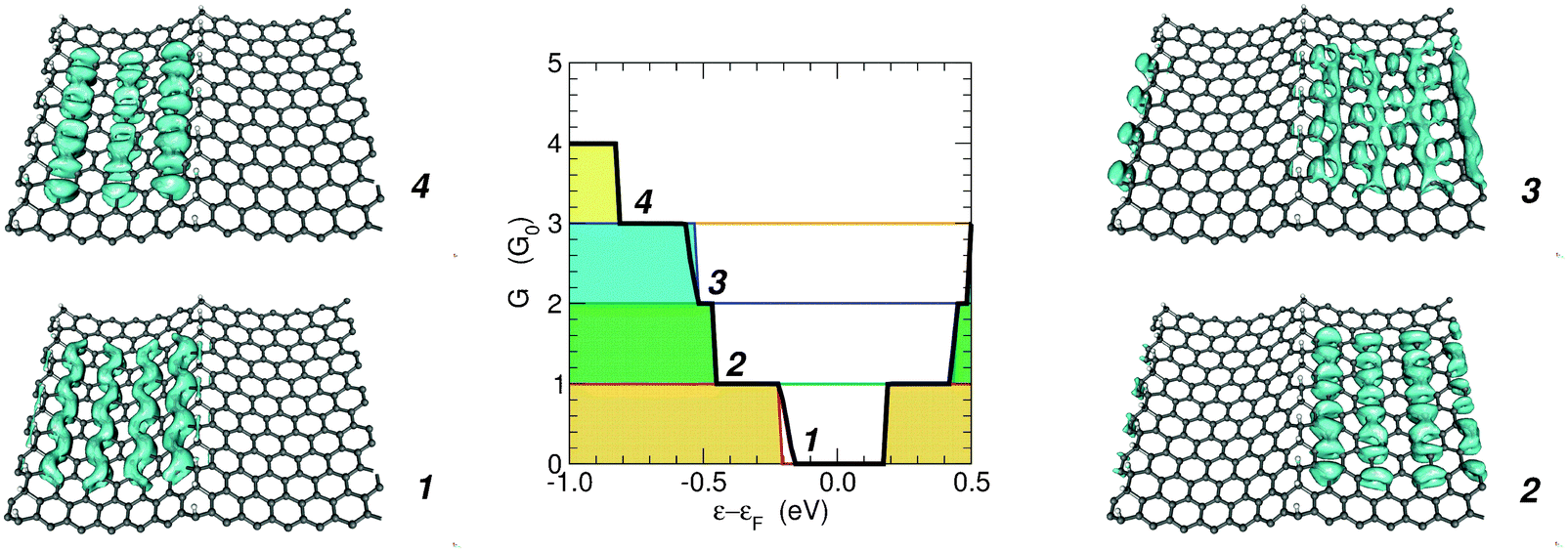
Relaxed structures were analyzed in detail by computing the band-structure and the corresponding density-of-states (DOS) per unit volume ρ(ε) as given by the Kohn–Sham Hamiltonian. Fig. 2 shows the DOS and the low energy band structure of the 6-SL structure, referenced to the Fermi level, along the path M–Γ–X, where M–Γ is perpendicular to the hydrogen-dimer lines and Γ–X along that line (see inset in Fig. 2). The structure features a small energy gap (of the order of 0.2 eV) at the Fermi level and a set of quasi-1D van Hove singularities which signal a vanishing dispersion perpendicularly to the dimer lines. Indeed, the band structure shows several states which are nearly flat along M–Γ and with quadratic or nearly conical dispersion along the Γ–X path. In the energy range of Fig. 2, there are five occupied (νh,m) and five unoccupied (νe,m) bands showing this behavior. They closely resemble the electronic states in armchair graphene nanoribbons, and form quasi-1D conduction channels appearing at quantized energies εm, approximately electron–hole symmetric. Actually, on closer inspection, the band structure closely resembles that of the corresponding armchair graphene nanoribbon which can be ‘cut out’ from the superlattice structure. This is shown in Fig. 2 where the band structure of the 11-aGNR is given as dashed lines, from Γ to X (in general, for the n-SL structure the relevant ribbon to compare with is the (2n − 1)-aGNR, where 2n − 1 gives the number of CC dimers across the GNR axis, as customary).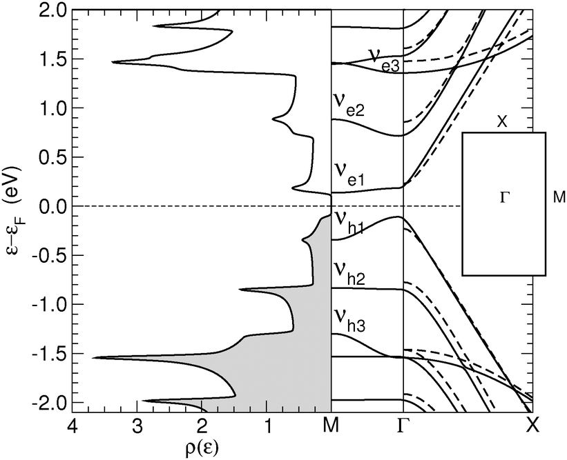 | ||
| Fig. 2 Density of states (left) and band structure (right, solid lines) of the 6-SL structure. The inset gives the superlattice Brillouin zone with its high symmetry points. Also shown in the right panel the band structure of the armchair nanoribbon cut out from the 6-SL structure and terminated with hydrogen atoms (dashed lines, from Γ to X). | ||
We further analyzed the spatial properties of the electronic states by looking at the Local Density of States (LDOS) ρ(x,ε) = 〈x|δ(ε − HKS)|x〉 which measures the weight of the system eigenstates at energy ε in a given point of space x. For the structure shown in Fig. 2 we evaluated the LDOS at several energies above and below the Fermi level, close to the van Hove singularities which mark the channel opening. An example is given in Fig. 3, where the isosurfaces of the LDOS at the energies of the νh,1 and νe,1 bands at the Γ point are reported. Note that they are clearly electron–hole symmetric, with the phase in one sublattice reverted when passing from h to e and the bond patterning changing accordingly.‡ The zeros of the localized state wave functions are clearly distinguished for m = 1 only because for m > 1 a number of states (with different kinetic energy along the channel) contribute to the LDOS.
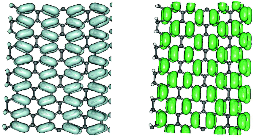 | ||
| Fig. 3 Isosurfaces of the local density of states evaluated in correspondence of the lowest energy van Hove singularity of Fig. 2, νh1 and νe1, in the left and right panels, respectively. | ||
Finally, the energy gap in n-SL structures is generally decreasing for increasing n, though the actual decay depends strongly on whether n = 3m, 3m + 1 or 3m + 2 (m integer), analogously to what happens in armchair nanoribbons.6,7 This is shown in Fig. 4 where the energy gap of several SL structures, as computed at the above level of theory, is reported as a function of n (for a comparison, notice that the number of CC dimers belongs to the 3m + 2, 3m + 1 and 3m sequences, respectively). Note in particular, that the sequence n = 3m has a gap which is almost unchanged with the width. The computed values agree reasonably well with those previously reported for these structures,24 once the differences in the DFT functionals adopted are taken into account.
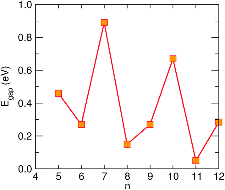 | ||
| Fig. 4 Dependence of the energy gap in n-SL structures as a function of n (orange symbols). | ||
Furthermore, we considered the energy gap of several (n1,n2)-SL structures and found, in agreement with the dispersionless behavior along M–Γ, that it is always given, to a good approximation, by the ni-SL with the smallest gap. This supports the idea that the conduction channels are independent of each other, as we detail in the next section by showing the results of our transport calculations.
3.2 Transport across and along the channels
Transport calculations were performed on channels of finite length, periodically repeated in the directions perpendicular to the transport direction, according to the geometry depicted in Fig. 5 for the case of transport along the hydrogen-dimer lines in the (6,11)-SL structure (i.e. along an armchair line). Similarly for transport perpendicular to the hydrogen-dimer lines, with y playing the role of transport direction and the electrodes placed on the left and right sides of the slab reported in Fig. 5.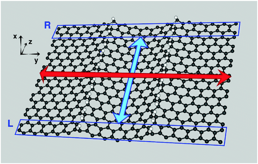 | ||
| Fig. 5 Geometry adopted for transport calculation along the hydrogen-dimer lines (z axis) in the (6,11)-SL structure, showing the left (L) and right (R) electrodes as rectangles. The large arrows mark the width (red) and length (cyan) of the scattering region. The system is periodic along x, y, with a ∼20 Å wide vacuum along x. | ||
Fig. 6 reports the zero-bias cumulative transmission function N(ε) ≡ G(ε)/G0 of 6-SL structures, both along the hydrogen-dimer lines and perpendicular to them. The results refer to a single unit cell along (x, y), and were obtained with a fine k-mesh containing 100 k-points parallel to the slab. It is evident from this figure that electronic transport is strongly anisotropic, with a nearly vanishing transmission probability perpendicular to the lines, despite the presence of a single hydrogen-dimer line to be crossed. In contrast, transport along the dimer lines occurs without scattering and the transmission function shows an almost perfect step-like behavior as expected when transmission modes progressively open. Similar results were obtained for different SL structures considered, and thus in the following we focus only on the case where transport occurs parallel to the hydrogen lines.
 | ||
| Fig. 6 Conductance function for the 6-SL structure along the hydrogen-dimer lines (red) and perpendicularly to them (black). The latter values have been multiplied by a factor of 10 for clarity. | ||
In general, transport along the dimer lines remains rather simple in all the n-SL structures: the step-like behavior of N(ε) marks the opening of transport channels, with a step occurring at any energy where a transverse mode appears. The height of each step reaches its maximum (usually corresponding to one perfectly conducting channel) in the very small energy window where dispersion along the transverse direction occurs.
Less trivial results are obtained upon combining superlattices with different widths, and exploiting their different electronic properties (energy gap). For instance Fig. 7 reports the transmission results for the (6,7)-SL structure, along with its band structure. Notice that in this case, the energy gap of the constituent 7-SL structure is about 0.5 eV larger than that of the 6-SL one, despite its larger width (see Fig. 4). As a consequence, the gap in the transmission function closely resembles that in the constituent 6-SL structure (Fig. 6, and black lines in Fig. 7), while the steps mainly follow the denser energy levels of the 7-SL structure. In fact, on closer inspection, the transmission function of the compound (6,7)-SL structure is given, to a very good approximation, by the sum of the transmission in the two constituent structures, the 6- and 7-SL structures. This was similar for all the compound structures we considered (not reported).
 | ||
| Fig. 7 Band structure (left) and conductance function (right) for transport along the hydrogen-dimer lines of the (6,7)-SL structure. Also shown in the right panel are the results of the constituent 6-SL structure (black) for comparison. | ||
Stated differently, the channels confined by the hydrogen-dimer lines essentially act as independent conduction channels, i.e. as resistors in parallel, as a consequence of the weakly dispersing character of the energy bands along the direction transverse to the dimer line. Thus, hydrogen-dimer lines work as hard-wall confining potentials for the electrons in graphene, much like the presence of edges in nanoribbon geometries.
3.3 Transmission eigenchannels
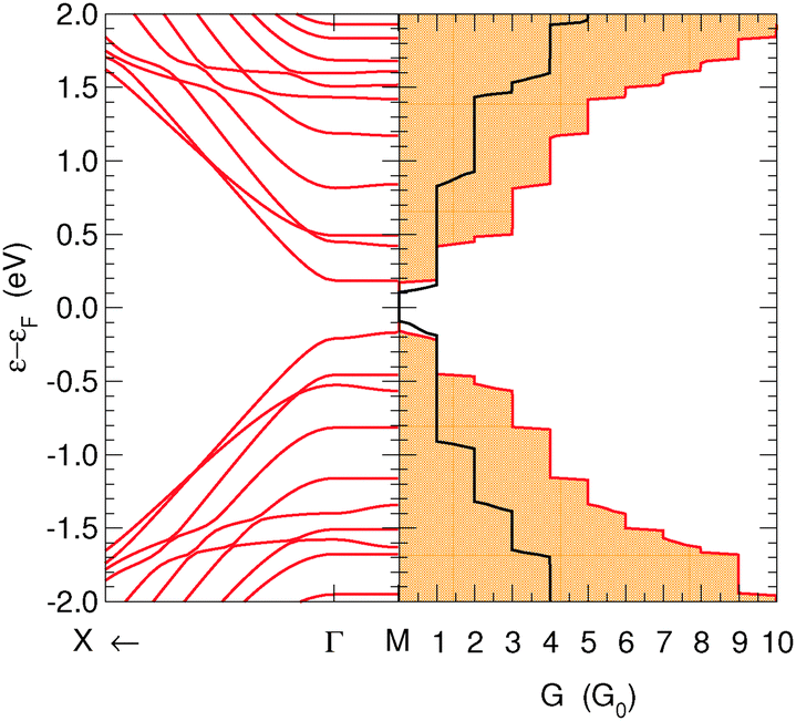
The above considerations suggest that the conduction properties of the channels confined by hydrogen-dimer lines are superimposable because conduction channels are spatially separated. To check this we computed the transmission eigenchannels at the Γ point for a number of selected energies below the Fermi level (notice though that the results for the square moduli of the transmission channels are insensitive to the exact value of the energy, in the range where they transmit).Fig. 8 shows how the eigen-transmissions in the (6,7)-SL structure sum up to give the cumulative transmission probability: they are perfectly conducting channels with different threshold energies (i.e. t(ε) ≡ 1 when the channel is open). Correspondingly, the eigenchannels localize in different superlattice regions, according to the band structure of the constituent elements. For instance, the first and fourth steps in the conductance function are due to the energy levels in the 6-SL structure (see also Fig. 7) and the corresponding eigenchannels localize in the six-unit-wide canal.
 | ||
| Fig. 8 Middle panel: the conductance function of the (6,7)-SL structure (solid black line), along with the eigen-transmissions computed at Γ, offset by one unit each for clarity. Red, green, blue and orange lines for eigen-channels m = 1–4, respectively. Left and right panels: the corresponding eigen-channels (square moduli) at ∼1 eV below the Fermi level. | ||
These results confirm that confinement is indeed at work in electronic transport and that each section defined by a pair of hydrogen-dimer lines acts as an independent transport channel, as previously suggested by the spatial distribution of the HOMO–LUMO in multiple period structures22 (compare also Fig. 3 with the m = 1 eigenchannel reported in Fig. 8).
3.4 I–V characteristic
Finally, we analyze the effect that finite bias voltages VSD have on the transmission functions. Fig. 9 shows the results obtained for the (6,7)-SL structure at different bias voltages (VSD = 0.25, 0.50, 0.75 and 1.00 V), well beyond the size of the band-gap of this structure.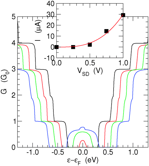 | ||
| Fig. 9 Conductance function of the (6,7)-SL structure for different bias voltages, VSD. Black, red, green and blue curves for VSD = 0.25, 0.50, 0.75 and 1.00 V, respectively. The inset shows the computed I–V characteristic (black symbols) along with its cubic fit (red). | ||
As expected, the effect of the bias is rather simple: the potential drop inside the channel occurs smoothly from one electrode to the other, and determines a band-mismatch between the left and right ends. As a consequence, the shape of the conductance function is simply determined by an overlap requirement and can be calculated to a good approximation as G(ε,VSD) = min{G(ε − |e|VSD/2,0),G(ε + |e|VSD/2,0)}.
An exception is for energies within the gap region, where transport can occur, depending on the channel length, from the valence band of one end to the conduction band of the other end, upon tunneling through the gap region. Thus, the peak at the center of the conductance spectrum reflects the increase of tunneling probability that occurs when the barrier width decreases as a consequence of a bias increase. In this regime, the transistor simply breaks down, and the total current has an approximately cubic increase, which fits well to Simmons' tunneling in the intermediate-voltage range,42I ≈ JL(V + γV3). This is shown in the inset of Fig. 9 which reports the I–V characteristic obtained with the above bias values.
4 Summary and conclusions
We reported on the electronic and transport properties of a family of hydrogen-dimer line structures, one of which has been recently realized on graphite after hydrogen treatment of a monolayer of cyanuric acid self-assembled on the surface. The electronic structure of these ordered hydrogenated domains agrees with previous theoretical results suggesting that hydrogen-dimer lines could behave as hard-wall confinement potentials for the electron, and turn graphene into (armchair) nanoribbons. We support this interpretation with the results of NEGF-DFT transport calculations on several single and compound structures, which show conductance plateaus clearly related to the states which are confined in between the dimer lines, as further confirmed by the spatial properties of the transmission eigenchannels.All this suggests that hydrogen-dimer lines may represent a valid alternative to graphene nano-ribbons to be used in one and the same support for fabricating (chemically imprinting) integrated nano-circuits. Such lines may be used to define insulating layers and create electron waveguides (as exemplified by a (n1,n2)-SL structure with n1 small – the insulating sections – and n2 ≫ n1 – the electron waveguides), or to draw semiconducting ribbons (when n is sufficiently small), provided transverse lines are introduced in the remaining armchair directions to block conduction outside the channel.
References
- K. S. Novoselov, A. K. Geim, S. V. Morozov, D. Jiang, Y. Zhang, S. V. Dubonos, I. V. Gregorieva and A. A. Firsov, Science, 2004, 306, 666 CrossRef CAS PubMed.
- A. H. Castro Neto, F. Guinea, N. M. R. Peres, K. S. Novoselov and A. K. Geim, Rev. Mod. Phys., 2009, 81, 109 CrossRef CAS.
- N. M. R. Peres, Rev. Mod. Phys., 2010, 82, 2673 CrossRef CAS.
- D. S. L. Abergel, V. Apalkov, J. Berashevich, K. Ziegler and T. Chakraborty, Adv. Phys., 2010, 59, 261 CrossRef CAS.
- M. Katsnelson, Graphene: Carbon in Two Dimensions, Cambridge University Press, 2012 Search PubMed.
- K. Wakabayashi, M. Fujita, H. Ajiki and M. Sigrist, Phys. Rev. B: Condens. Matter Mater. Phys., 1999, 59, 8271–8282 CrossRef CAS.
- Y. W. Son, M. L. Cohen and S. G. Louie, Phys. Rev. Lett., 2006, 97, 216803 CrossRef.
- R. Saito, G. Dresselhaus and M. S. Dresselhaus, Physical Properties of Carbon Nanotubes, Imperial College Press, London, 1999 Search PubMed.
- M. S. Dresselhaus, G. Dresselhaus and P. Avouris, Carbon Nanotubes: Synthesis, Structure, Properties and Applications, Springer, Berlin, 2001 Search PubMed.
- F. Schwierz, Nat. Nanotechnol., 2010, 5, 487 CrossRef CAS PubMed.
- L. Xie, L. Jiao and H. Dai, J. Am. Chem. Soc., 2010, 132, 14751 CrossRef CAS PubMed.
- X. Zhang, O. V. Yazyev, J. Feng, L. Xie, C. Tao, Y.-C. Chen, L. Jiao, Z. Pedramrazi, S. G. Louie, H. Dai and M. F. Crommie, ACS Nano, 2013, 7, 198 CrossRef CAS PubMed.
- J. Cai, P. Ruffieux, R. Jaafar, M. Bieri, T. Braun, S. Blankenburg, M. Muoth, A. Seitsonen, M. Saleh, X. Feng, K. Müllen and R. Fasel, Nature, 2010, 466, 470 CrossRef CAS PubMed.
- Y.-C. Chen, D. G. de Oteyza, Z. Pedramrazi, C. Chen, F. R. Fischer and M. F. Crommie, ACS Nano, 2013, 7, 6123–6128 CrossRef CAS PubMed.
- P. B. Bennett, Z. Pedramrazi, A. Madani, Y.-C. Chen, D. G. de Oteyza, C. Chen, F. R. Fischer, M. F. Crommie and J. Bokor, Appl. Phys. Lett., 2013, 103, 253114 CrossRef PubMed.
- J. A. Fürst, J. G. Pedersen, C. Flindt, N. A. Mortensen, M. Brandbyge, T. G. Pedersen and A.-P. Jauho, New J. Phys., 2009, 11, 095020 CrossRef.
- R. Martinazzo, S. Casolo and G. F. Tantardini, Phys. Rev. B: Condens. Matter Mater. Phys., 2010, 81, 245420 CrossRef.
- V. M. Pereira, J. M. B. Lopes dos Santos and A. H. Castro Neto, Phys. Rev. B: Condens. Matter Mater. Phys., 2008, 77, 115109 CrossRef.
- O. V. Yazyev, Rep. Prog. Phys., 2010, 73, 056501 CrossRef.
- R. Martinazzo, S. Casolo and G. F. Tantardini, in Physics and Applications of Graphene – Theory, ed. S. Mikhailov, InTech, 2011, ch. 3 Search PubMed.
- L. Chernozatonskii, P. Sorokin, E. A. Belova, J. Brüning and A. Fedorov, JETP Lett., 2007, 85, 77 CrossRef CAS.
- L. Chernozatonskii, P. Sorokin and J. Brüning, Appl. Phys. Lett., 2007, 91, 183103 CrossRef PubMed.
- L. A. Chernozatonskii and P. Sorokin, Phys. Status Solidi B, 2008, 10, 2086 CrossRef.
- L. A. Chernozatonskii and P. B. Sorokin, J. Phys. Chem. C, 2010, 114, 3225 CAS.
- J. T. Rasmussen, T. Gunst, P. Bløggild, A.-P. Jauho and M. Brandbyge, Beilstein J. Nanotechnol., 2013, 4, 103 CrossRef PubMed.
- D. Gunlycke, S. Vasudevan and C. T. White, Nano Lett., 2012, 13, 259 CrossRef PubMed.
- L. Hornekær, E. Rauls, W. Xu, Ž. Šljivančanin, R. Otero, I. Stensgaard, E. Læegsgaard, B. Hammer and F. Besenbacher, Phys. Rev. Lett., 2006, 97, 186102 CrossRef.
- S. Casolo, O. M. Løvvik, R. Martinazzo and G. F. Tantardini, J. Chem. Phys., 2009, 130, 054704 CrossRef PubMed.
- R. Balog, B. Jørgensen, J. Wells, E. Lægsgaard, P. Hofmann, F. Besenbacher and L. Hornekær, J. Am. Chem. Soc., 2009, 25, 131 Search PubMed.
- D. C. Elias, R. R. Nair, T. M. G. Mohiuddin, S. V. Morozov, P. Blake, M. P. Halsall, A. C. Ferrari, D. W. Boukhvalov, M. I. Katsnelson, A. K. Geim and K. S. Novoselov, Science, 2009, 323, 610–613 CrossRef CAS PubMed.
- A. Bostwick, J. L. McChesney, K. V. Emtsev, T. Seyller, K. Horn, S. D. Kevan and E. Rotenberg, Phys. Rev. Lett., 2009, 103, 056404 CrossRef.
- E. N. Voloshina, E. Fertitta, A. Garhofer, F. Mittendorfer, M. Fonin, A. Thissen and Y. S. Dedkov, Nat. Sci. Rep., 2013, 3, 1072 CAS.
- R. Balog, B. Jørgensen, L. Nilsson, M. Andersen, E. Rienks, M. Bianchi, M. Fanetti, E. Lægsgaard, A. Baraldi, S. Lizzit, Z. Šljivančanin, F. Besenbacher, B. Hammer, T. G. Pedersen, P. Hofmann and L. Hornekær, Nat. Mater, 2010, 9, 315 CrossRef CAS PubMed.
- L. Nilsson, Z. Šljivančanin, R. Balog, W. Xu, T. R. Linderoth, E. Lægsgaard, I. Stensgaard, B. Hammer, F. Besenbacher and L. Hornekær, Carbon, 2012, 50, 2052 CrossRef CAS PubMed.
- J. P. Perdew, K. Burke and M. Ernzerhof, Phys. Rev. Lett., 1996, 77, 3865 CrossRef CAS.
- J. P. Perdew, K. Burke and M. Ernzerhof, Phys. Rev. Lett., 1997, 78, 1396 CrossRef CAS.
- N. Troullier and J. L. Martins, Phys. Rev. B: Condens. Matter Mater. Phys., 1991, 43, 1993–2006 CrossRef CAS.
- S. G. Louie, S. Froyen and M. L. Cohen, Phys. Rev. B: Condens. Matter Mater. Phys., 1982, 26, 1738–1742 CrossRef CAS.
- J. M. Soler, E. Artacho, J. D. Gale, A. García, J. Junquera, P. Ordejón and D. Sánchez-Portal, J. Phys.: Condens. Matter, 2002, 14, 2745 CrossRef CAS.
- H. J. Monkhorst and J. D. Pack, Phys. Rev. B: Solid State, 1976, 13, 5188 CrossRef.
- M. Brandbyge, J. L. Mozos, P. Ordejón, J. Taylor and K. Stokbro, Phys. Rev. B: Condens. Matter Mater. Phys., 2002, 65, 165401 CrossRef.
- J. Cuevas and E. Scheer, Molecular electronics: an introduction to theory and experiments, World Scientific, 2010 Search PubMed.
- M. Paulsson and M. Brandbyge, Phys. Rev. B: Condens. Matter Mater. Phys., 2007, 76, 115117 CrossRef.
- T. Frederiksen, M. Paulsson, M. Brandbyge and A.-P. Jauho, Phys. Rev. B: Condens. Matter Mater. Phys., 2007, 75, 205413 CrossRef.
- M. Paulsson and T. Frederiksen, Inelastica, a Python package for SIESTA/TranSIESTA DFT codes, http://sourceforge.net/projects/inelastica Search PubMed.
Footnotes |
| † Electronic supplementary information (ESI) available. See DOI: 10.1039/c4cp01025f |
| ‡ Electron–hole symmetry implies that the phase of the wavefunction on one sublattice is reverted when moving from electrons to holes, i.e. if ψ = ϕA + ϕB is the wavefunction at a given energy ε and ϕA, ϕB its amplitudes on the A, B sublattices, then ϕ = ϕA − ϕB is its e–h counterpart at energy −ε. |
| This journal is © the Owner Societies 2014 |