 Open Access Article
 This Open Access Article is licensed under a Creative Commons Attribution-Non Commercial 3.0 Unported Licence
Selective adsorption of bismuth telluride nanoplatelets through electrostatic attraction†
Lingling
Guo
ab,
Amira
Aglan
ab,
Haiyu
Quan
ab,
Junjie
Sun
bc,
Chaolong
Tang
bd,
Jinhui
Song
bd,
Greg
Szulczewski
be and
Hung-Ta
Wang
*ab
aDepartment of Chemical and Biological Engineering, University of Alabama, Tuscaloosa, AL 35487, USA. E-mail: htwang@eng.ua.edu
bCenter for Materials for Information Technology (MINT Center), University of Alabama, Tuscaloosa, AL 35487, USA
cSchool of Physics, Shandong University, Jinan, Shandong 250100, China
dDepartment of Metallurgical and Materials Engineering, University of Alabama, Tuscaloosa, AL 35487, USA
eDepartment of Chemistry, University of Alabama, Tuscaloosa, AL 35487, USA
First published on 23rd April 2014
Abstract
We demonstrate a facile technique to assemble solution phase-synthesized bismuth telluride (Bi2Te3) nanoplatelets into arrays of micropatterns. Aminosilane self-assembled monolayers (SAMs) are printed on silicon dioxide (SiO2) substrates using microcontact printing (μCP). The SAM printed surfaces are terminated with amine-groups allowing Bi2Te3 nanoplatelet selective adsorption by electrostatic attraction. Using Kelvin probe force microscopy, the electrical potential difference between aminosilane SAM and Bi2Te3 nanoplatelet surfaces is found to be ∼650 mV, which is larger than that (∼400 mV) between the SiO2 substrate and Bi2Te3 nanoplatelet surfaces. The selective adsorption provides an opportunity for integrating solution phase-grown topological insulators toward several device-level applications.
1. Introduction
The V–VI group chalcogenides, including bismuth telluride (Bi2Te3), bismuth selenide (Bi2Se3), and antimony telluride (Sb2Te3), are three-dimensional topological insulators, whose surfaces are covered by the two-dimensional electron gas (2DEG) from the topological surface states.1–6 The novel topological surface states are induced by a strong spin–orbit coupling, and the spin carriers are protected against time reversal perturbations, e.g., surface defects and impurities, making the 2DEG spin charge transport essentially dissipation-less.7 Recent advances in topological insulator research have drawn much attention due to its potential application8 in the next generation electronics,9,10 thermoelectrics,11–14 infrared detectors,15 and heterogeneous catalysis.16The nontrivial topological surface states of these V–VI group chalcogenides are derived from their unique layered crystal structure. In Bi2Te3, five atomic layers in the order of Te(1)–Bi–Te(2)–Bi–Te(1) form a charge neutral sheet with a thickness of ∼1 nm, called a quintuple sheet.17,18 Stacking quintuple sheets along the c-axis forms the rhombohedral structure, which is in the D53d(R![[3 with combining macron]](https://www.rsc.org/images/entities/char_0033_0304.gif) m) space group.19,20 The adjacent Bi and Te atomic layers in a quintuple sheet are held by covalent forces; in contrast, the bonding between neighboring quintuple layers, i.e., between adjacent Te(1) atomic layers, is a weak van der Waals interaction.17,18 Because Bi2Se3 has a smaller van der Waals gap than Bi2Te3 and Sb2Te3, the spin–orbit coupling in Bi2Se3 is stronger, and consequently the electronic structures of topological surface states in these V–VI group chalcogenides are also different.2 Topological surface states in several V–VI group chalcogenides have been revealed by angle-resolved photoemission spectroscopy,1,3,4 scanning-tunneling microscopy,7 and transport measurements.5,6 Currently, the major challenge hampering the novel 2DEG toward practical applications is that the surface spin charge transport is overwhelmed by the ordinary bulk charges. On the other hand, there is a lack of processing techniques suitable for a large scale, device-level integration.
m) space group.19,20 The adjacent Bi and Te atomic layers in a quintuple sheet are held by covalent forces; in contrast, the bonding between neighboring quintuple layers, i.e., between adjacent Te(1) atomic layers, is a weak van der Waals interaction.17,18 Because Bi2Se3 has a smaller van der Waals gap than Bi2Te3 and Sb2Te3, the spin–orbit coupling in Bi2Se3 is stronger, and consequently the electronic structures of topological surface states in these V–VI group chalcogenides are also different.2 Topological surface states in several V–VI group chalcogenides have been revealed by angle-resolved photoemission spectroscopy,1,3,4 scanning-tunneling microscopy,7 and transport measurements.5,6 Currently, the major challenge hampering the novel 2DEG toward practical applications is that the surface spin charge transport is overwhelmed by the ordinary bulk charges. On the other hand, there is a lack of processing techniques suitable for a large scale, device-level integration.
Previously, Bi2Te3 and Bi2Se3 nanoplatelets were synthesized on mica surfaces by a chemical vapor transport (CVT) method.21 On the atomically-smooth surfaces, the nanoplatelet growth could be controlled precisely along mica's crystal orientation via the van der Waals epitaxy. Later, arrays of nanoplatelets as flexible infrared transparent electrodes were also demonstrated.22 Although the van der Waals epitaxy on mica substrates is suitable for selective growth of chalcogenide-based topological insulators, mica substrates are incompatible with common silicon manufacturing processes, which will limit their use in many applications. In contrast, solvothermal syntheses of Bi2Te3 nanoplatelets are facile, and nanoplatelets can be transferred to any substrate. As a result, it is important to develop methods for transferring Bi2Te3 nanoplatelets to well-defined positions on the silicon substrate to advance the potential applications of these topological insulator nanoplatelets.
In this work, we report a practical technique to assemble solution phase-grown Bi2Te3 nanoplatelets into micropattern arrays by the microcontact printing (μCP) technique.23–25 We demonstrate that Bi2Te3 nanoplatelets could selectively adsorb onto the surfaces of aminosilane self-assembled monolayers (SAMs) that were printed on silicon oxide (SiO2) substrates using μCP. We used Kevin probe force microscopy (KPFM) to characterize the surface electrical potentials and measured a ∼650 mV potential difference between aminosilane SAMs and Bi2Te3 nanoplatelets. The Coulombic interaction between the protonated amine groups and Bi2Te3 nanoplatelets enables a robust and scalable method for selectively adsorbing solution phase-grown topological insulator nanoplatelets into micropattern arrays. Such a selective adsorption of topological insulators by aminosilane SAMs also opens the possibilities for topological insulator surface passivation, reduction of ordinary bulk charges, and modification of topological surface states via electrostatic gating.26,27
2. Experimental
Several solvothermal syntheses of Bi2Te3 nanoplatelets were previously reported using different precursors and growth conditions in a similar reducing environment.28–32 Our method is based on the approach of Li and co-workers.28 The Bi2Te3 nanoplatelets were synthesized using the general autoclave reactor (23 ml) from Parr Instrument Company. Bismuth oxide (Bi2O3, 99.9995%), tellurium dioxide (TeO2, 99.9995%), ethylene glycol (EG, Reagent Grade), polyvinylpyrrolidone (PVP, average molecular weight 40![[thin space (1/6-em)]](https://www.rsc.org/images/entities/char_2009.gif) 000), and sodium hydroxide flakes (NaOH, 98.7%+) were all purchased from Alfa Aesar. All of the chemicals were used as received without further purification. In a typical synthesis, 0.1865 g of TeO2, 0.1793 g of Bi2O3, 0.3044 g of PVP, and 0.3047 g of NaOH were added into 15 ml of EG. The mixture was stirred vigorously at 90 °C for 30 minutes in order to thoroughly dissolve the chemicals in EG. The precursor solution was sealed in the autoclave reactor, and the solvothermal reaction was carried out in the oven at a temperature of 210 °C for 24 hours. The as-grown nanoplatelets were collected by centrifugation, and cleaned by rinsing alternatively in de-ionized (DI) water at room temperature and 1-methyl-2-pyrrolidone (NMP) at 85 °C for five cycles. It was critical to remove PVP thoroughly to obtain clean Bi2Te3 nanoplatelet surfaces for the selective adsorption. The good solubility of PVP in NMP is likely due to the fact that NMP is the pendant group of the polymer, PVP. At an elevated temperature (85 °C), the solubility of PVP in NMP can be further increased. The cleaned Bi2Te3 nanoplatelets were characterized by scanning electron microscopy (SEM, JEOL 7000 FE), X-ray diffraction (XRD, Bruker D8 Discover), atomic force microscopy (AFM, Park XE 70), and transmission electron microscopy (TEM, FEI Tecnai F-20).
000), and sodium hydroxide flakes (NaOH, 98.7%+) were all purchased from Alfa Aesar. All of the chemicals were used as received without further purification. In a typical synthesis, 0.1865 g of TeO2, 0.1793 g of Bi2O3, 0.3044 g of PVP, and 0.3047 g of NaOH were added into 15 ml of EG. The mixture was stirred vigorously at 90 °C for 30 minutes in order to thoroughly dissolve the chemicals in EG. The precursor solution was sealed in the autoclave reactor, and the solvothermal reaction was carried out in the oven at a temperature of 210 °C for 24 hours. The as-grown nanoplatelets were collected by centrifugation, and cleaned by rinsing alternatively in de-ionized (DI) water at room temperature and 1-methyl-2-pyrrolidone (NMP) at 85 °C for five cycles. It was critical to remove PVP thoroughly to obtain clean Bi2Te3 nanoplatelet surfaces for the selective adsorption. The good solubility of PVP in NMP is likely due to the fact that NMP is the pendant group of the polymer, PVP. At an elevated temperature (85 °C), the solubility of PVP in NMP can be further increased. The cleaned Bi2Te3 nanoplatelets were characterized by scanning electron microscopy (SEM, JEOL 7000 FE), X-ray diffraction (XRD, Bruker D8 Discover), atomic force microscopy (AFM, Park XE 70), and transmission electron microscopy (TEM, FEI Tecnai F-20).
The elastic poly(dimethylsiloxane) (PDMS) stamps for the μCP were fabricated by first mixing a Sylgard 184 elastomer and a curing agent (w/w = 10/1) and pouring the mixture over master substrates, which were fabricated by conventional photolithography (Karl Suss MA6) with either the SU8-3025 resist or the Shipley 1818 resist. After baking at 70 °C for 24 hours, the PDMS was peeled off from the master and cut into a 2 × 2 cm stamp. To make the μCP ink, (3-aminopropyl)trimethoxysilane (APTMS, 97% from Sigma-Aldrich) was diluted in DI water to 1% by volume, sonicated for 3 minutes, and then filtered through a syringe filter (0.2 μm pore size, from VWR). In a standard μCP process, the PDMS stamp was immersed in the filtered 1% APTMS aqueous solution for 2 minutes and then dried by nitrogen blow. The substrate was an n-type (100) silicon substrate (phosphorus doped, resistivity = 0.001–0.005 ohm cm) with a thermally-grown dry oxide (thickness ∼ 120 nm), which was cleaned by rinsing with acetone–IPA, and oxygen plasma treatment before the μCP. The stamp was brought in contact with the SiO2/Si substrate for 10–20 s at 50 °C on the hotplate to ensure the transfer of a single molecular layer of APTMS. The APTMS printed substrate was immediately immersed in the Bi2Te3 nanoplatelet-dispersed aqueous solution for 2–20 minutes under a mild vortex action. Finally, the substrate was rinsed with DI water and blown dry by a nitrogen gun. The nanoplatelet-dispersed aqueous solution used for the adsorption was prepared by diluting 20 μl of highly concentrated, cleaned nanoplatelet solution in 2 ml of DI water, followed by vortex and sonication until a homogeneous nanoplatelet dispersion with a light grey color is obtained. SEM, AFM, and KPFM were used to characterize the APTMS printed and nanoplatelet-adsorbed samples.
3. Results and discussion
Fig. 1 presents the structure and chemical characterization of the solution phase-grown Bi2Te3 nanoplatelets. As shown by SEM (Fig. 1(a and d)), the Bi2Te3 nanoplatelets have a hexagonal morphology owing to the atomic hexagonal packing in their crystal structure. Interestingly, roughly 50% nanoplatelets have a hole in the center, which may originate from the growth of a heterostructure of Bi2Te3 nanoplatelets skewered by a Te nanowire as observed in the previous reports.28,29,32 It is likely that when Te nanowires are dissolved by NaOH, Bi2Te3 nanoplatelets are detached, leaving a hole in the nanoplatelet center. Quantitative analysis of the EDS spectrum (Fig. 1(b)) yields the atomic composition of Bi and Te to be 39.55% and 60.45%, respectively. The XRD pattern (Fig. 1(c)) of the as-synthesized Bi2Te3 nanoplatelets can be indexed with the rhombohedral Bi2Te3 crystal, and is consistent with the standard data file (PDF card no. 15-0863). In Fig. 1(e), high resolution TEM (HRTEM) and selected area electron diffraction (SAED) performed on the Bi2Te3 nanoplatelet show clear lattice fringes and patterns of hexagonally-symmetric spots, respectively. The AFM topographic image (Fig. 1(f)) indicates that the lateral size of the nanoplatelets is roughly in the range of 500 nm to 3 μm, and the thickness is about 10–100 nm. Collectively, the HRTEM, SAED, and XRD data indicate that our solvothermal synthesis produced highly crystallized Bi2Te3 nanoplatelets, which is consistent with the report of Li et al.28 | ||
| Fig. 1 (a) SEM image of the cleaned Bi2Te3 nanoplatelets. Inset: photograph of the vials with as-grown and cleaned nanoplatelet solution. (b) EDS and (c) XRD of cleaned Bi2Te3 nanoplatelets. (d) High magnification SEM image of the Bi2Te3 nanoplatelet. (e) TEM image of the Bi2Te3 nanoplatelet. Insets are HRTEM and SAED, respectively. (f) AFM topographic image of the Bi2Te3 nanoplatelets with their thicknesses labeled accordingly. | ||
We note that cleaned Bi2Te3 nanoplatelets have a low affinity for SiO2 surfaces using either drop casting or dip coating. A low nanoplatelet coating density was consistently obtained, and it showed trivial dependencies on the nanoplatelet dispersion concentration, transferring (adsorption) time, and SiO2 substrate hydrophobic/hydrophilic properties. When a high concentration Bi2Te3 nanoplatelet dispersion was applied, nanoplatelets tended to aggregate to form clusters in local regions (i.e., nanoplatelets randomly pile up), and most areas were still covered with a low density of nanoplatelets. The low affinity between the Bi2Te3 nanoplatelets and SiO2 surfaces reveals a great challenge in assembling nanoplatelets for practical applications.
To provide a feasible solution, we printed SAMs of APTMS, which were expected to have a strong affinity for the Bi2Te3 nanoplatelet surface. Fig. 2 demonstrates the selective adsorption of Bi2Te3 nanoplatelets using the logo of the University of Alabama. The area of the logo “A” consists of an array of APTMS printed houndstooth patterns, and Bi2Te3 nanoplatelets were adsorbed mainly onto the APTMS printed regions. Interestingly, nanoplatelet aggregation (or stacking) frequently observed before was greatly reduced. More importantly, the selective adsorption can be consistently obtained, and the nanoplatelet coating density could be tuned by varying the adsorption time (shown in the ESI†). This general μCP of SAMs of aminosilane was first reported for the selective adsorption of negatively-charged nanomaterials by Zhang et al.23 Despite a ∼50% self-catalyzed hydrolysis of (3-aminopropyl)triethoxysilane (APTES) in aqueous solutions at room temperature,33,34 Zhang et al. demonstrated that using hydrophobic PDMS stamps with aqueous APTES inks could still print APTES monolayers. Although the printed APTES did not entirely form SAMs as noted in their work, the amine group terminated surfaces were very effective for the selective adsorption of citrate-coated Au nanoparticles and negatively-charged graphene oxide nanosheets. It is believed that due to an electrostatic interaction, the negatively-charged nanoparticles/nanosheets are attracted by the positively-charged, protonated amine group surfaces, resulting in a controllable adsorption.23,35 We demonstrate that this general μCP technique is very suitable to selectively adsorb topological insulator nanoplatelets.
 | ||
| Fig. 2 (a) Photograph of the silicon chip with selective adsorption of Bi2Te3 nanoplatelets to reveal logo “A” in which the area consists of a houndstooth array. (b) SEM image of Bi2Te3 nanoplatelets selective adsorption onto the houndstooth array that is in a local region of logo “A” shown in (a). (c) SEM image of a houndstooth pattern with APTMS coating via μCP, as illustrated by the cartoon. The dark region is the APTMS coating. (d) SEM image of a houndstooth pattern with the Bi2Te3 nanoplatelet adsorption, as illustrated by the cartoon. The white dots are nanoplatelets, as magnified in the SEM inset. | ||
Although the Bi2Te3 nanoplatelet selective adsorption could originate from a similar electrostatic interaction, we observed that Bi2Te3 nanoplatelets had a distinct adsorption behavior than Au nanoparticles.23,35 By immersing APTMS printed substrates in Bi2Te3 nanoplatelet dispersed aqueous solutions, a low density of Bi2Te3 nanoplatelet adsorption with a poor selectivity was obtained surprisingly. In contrast, when a mild vortex was applied during the adsorption of Bi2Te3 nanoplatelets and while other μCP conditions were kept the same, the adsorption density was greatly increased and the adsorption selectivity was also improved. Owing to the hexagonally-shaped nanoplatelet morphology, nanoplatelet adsorption onto a planar surface is limited to the top or bottom of nanoplatelet surfaces. When nanoplatelets were dispersed in an unstirred aqueous solution, the nanoplatelets were observed (in an optical microscope) to undergo a flipping-type motion. Owing to the flipping motion, dispersed nanoplatelets had a reduced chance to be in contact with APTMS printed surfaces using the top or bottom nanoplatelet surfaces, and consequently the chance of adsorption reduced. This is different to Au nanoparticle adsorption, as when any point of a sphere surface is in contact with a planar surface, adsorption would easily occur. Upon a mild vortexing-action, the Bi2Te3 nanoplatelets in the dispersed aqueous solution constantly collided with the substrate surface, so the chance for a face-to-face contact between nanoplatelet top/bottom surfaces and APTMS surfaces highly increased. At the same time, when nanoplatelets were in contact with bare SiO2 surfaces, the low affinity might not be strong enough to retain the adsorption, and nanoplatelets could be carried away by the vortex.
In order to obtain a stronger electrostatic interaction for Bi2Te3 nanoplatelet adsorption, we used in situ annealing during the μCP at a temperature of 50 °C. As shown in Fig. 3, the thickness of the APTMS coating clearly increased from 4–20 Å (μCP at room temperature) to 8–20 Å (μCP at 50 °C), and the density of APTMS also improved with the in situ annealing. It is clear that there are still APTMS particles with a height of ∼2 nm formed both with and without an in situ annealing, which is likely due to the condensation in the aqueous ink.23 Excluding those APTMS particles, it is shown that the average APTMS height is 4 Å without in situ annealing, and 8 Å with the in situ annealing. This implies that APTMS formed sub-monolayers at room temperature, while a better packing was preferred at 50 °C to produce a monolayer.33 It was previously reported that in toluene (i.e., no hydrolysis effect), in situ annealing at 70 °C could improve the packing quality of APTES on SiO2 surfaces.36 This is explained by the fact that the in situ annealing facilitates the formation of horizontal Si–O–Si bonds between adjacent APTES molecules, and the effect is an increased packing density. We suspect that the in situ annealing during μCP also improved the APTMS packing quality via a similar mechanism (i.e., formation of horizontal Si–O–Si bonds between APTMS). As the amine group density was increased from a closely packed APTMS SAM, Bi2Te3 nanoplatelet adsorption selectivity was achieved.
 | ||
| Fig. 3 AFM topographic images of the APTMS coating prepared by μCP for 10s (a) without, and (b) with 50 °C in situ annealing, respectively. The PDMS stamp contains an array of lines (line width × length = 1 × 100 μm). The topographic profiles (the green lines) are plotted and the scale bar is 1 nm. | ||
We further present the selective adsorption of Bi2Te3 nanoplatelets using stamps of either a 10 × 10 μm square array (as shown in Fig. 4(a and b)) or a 1 × 100 μm line array (as shown in Fig. 4(c and d)). Due to the softness of the PDMS and the dimensions of the square pillar array (shown in Fig. 4(a) inset), the PDMS stamps could sag and/or collapse to cause different μCP patterns.25 As shown in Fig. 4(a and b), the selective adsorption of Bi2Te3 nanoplatelets reveals the three μCP patterns, induced by the PDMS stamp (1) contacted normally, (2) collapsed plus sagged, and (3) collapsed only, respectively. This result shows that the selective adsorption could be robustly obtained on a 10 × 10 μm APTMS printed surface. To further test the robustness of the selective adsorption, we used PDMS stamps with the 1 × 100 μm line array. Fig. 4(c and d) show that Bi2Te3 nanoplatelets mainly adsorb onto the APTMS printed lines. Indeed, there are still un-wanted nanoplatelets adsorbed on the bare SiO2 surface due to the affinity between Bi2Te3 nanoplatelets and SiO2 surfaces. Nevertheless, it should be noted that the line width is comparable with the nanoplatelet lateral size, suggesting that under a vortex motion, the electrostatic interaction between Bi2Te3 nanoplatelets and APTMS printed surfaces is quite reliable to produce the nanoplatelet selective adsorption.
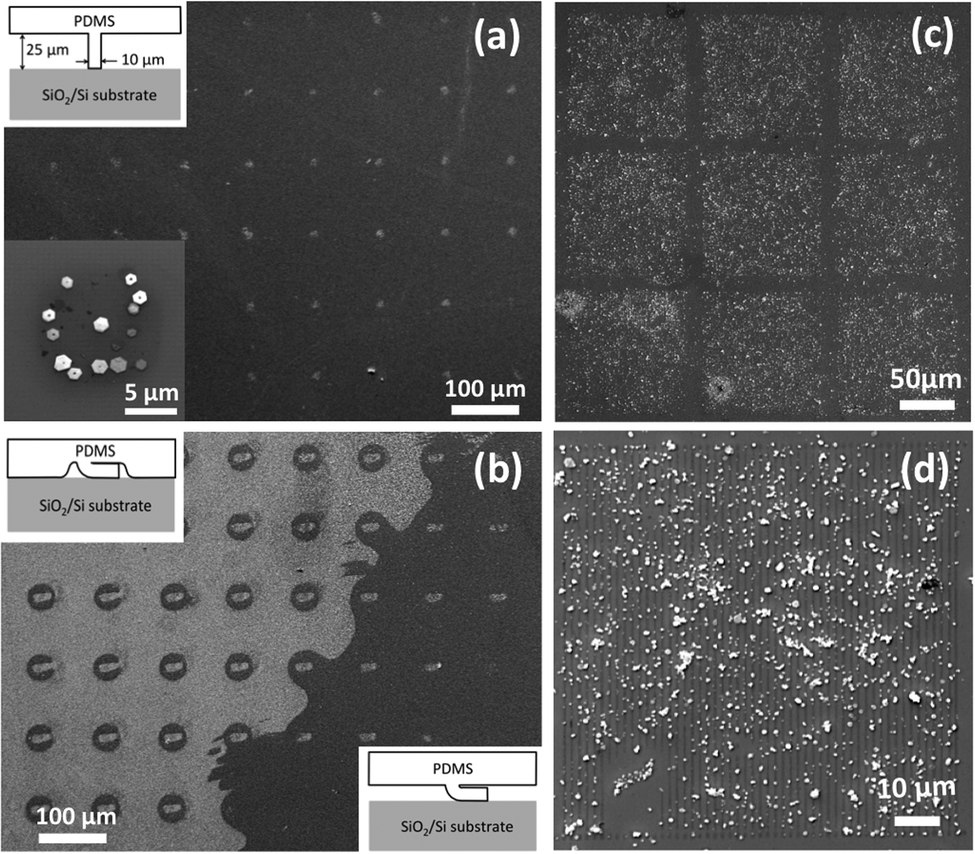 | ||
| Fig. 4 (a) SEM image of the selective adsorption of Bi2Te3 nanoplatelets using an array of 10 × 10 μm squares. The magnified SEM image (inset) shows that the nanoplatelets adsorbed onto the APTMS printed, a 10 × 10 μm square. The square pattern was obtained with the stamp in a normal contact, as illustrated in the inset. (b) SEM image of the selective adsorption of Bi2Te3 nanoplatelets reveals the two patterns printed with the stamp sagged plus collapsed (left region), and collapsed only (right region), respectively, as illustrated in the insets. Note that these two patterns and the square pattern shown in (a) were obtained from the same substrate. (c) SEM image of the selective adsorption using an array of 1 × 100 μm lines. (d) Magnified SEM image shows that Bi2Te3 nanoplatelets adsorbed mainly onto the APTMS printed lines. | ||
To understand the electrostatic interaction between the APTMS monolayer and the Bi2Te3 nanoplatelet surfaces, we examined the adsorbed Bi2Te3 nanoplatelets by KPFM. As shown in Fig. 5, the surface electrical potential difference between Bi2Te3 surfaces and APTMS printed surfaces is about 650 mV. In comparison, the surface electrical potential difference between Bi2Te3 surfaces and SiO2 surfaces is ∼400 mV, which is comparable to the report of Hao et al.37 It should be noted that the surface electrical potentials are measured under ambient conditions and not in an aqueous environment. With the existence of electrical double layers formed on the charged surfaces in an aqueous solution,38 the electrostatic forces experienced by the Bi2Te3 nanoplatelets during the adsorption should be quite different from what was measured by KPFM. Nevertheless, our data implied that in an aqueous solution, the electrostatic attraction force between APTMS surfaces and Bi2Te3 nanoplatelets was stronger than that between bare SiO2 surfaces and Bi2Te3 nanoplatelets, allowing the selective adsorption of Bi2Te3 nanoplatelets.
 | ||
| Fig. 5 (a) AFM topographic image of the Bi2Te3 nanoplatelets adsorbed on the APTMS printed, 10 × 10 μm square region. (b) Schematic of the electrical configuration for the Kevin probe force microscope measurement. (c) The electrical potential image is scanned in the same area as shown in (a). Note that all nanoplatelets are in the APTMS printed region, except the nanoplatelet in the left/bottom corner that is on the bare SiO2 surface. (d) The surface electrical potential profiles corresponding to the red and blue line marked in (c) are plotted, respectively. | ||
4. Conclusion
In summary, we have presented a practical method to selectively adsorb solution phase grown topological insulator nanoplatelets onto APTMS printed surfaces via μCP. Owing to the specific nanoplatelet morphology, vortex treatment during the adsorption facilitates the nanoplatelet adsorption and simultaneously improves the adsorption selectivity. We also show that APTMS monolayer packing can be improved by in situ annealing at 50 °C during μCP, which further enhances the nanoplatelet adsorption. The electrical potential difference, measured by KPFM, between aminosilane SAMs and Bi2Te3 nanoplatelet surfaces is larger than that between SiO2 and Bi2Te3 surfaces. We attribute the selective adsorption of Bi2Te3 nanoplatelets to this electrostatic interaction. Such a general adsorption of negatively-charged topological insulators is suitable for a large-scale assembly and device level fabrication.Acknowledgements
This work at the University of Alabama (UA) is supported by the UA start-up fund and the 2012 UA Research Grants Committee (RGC) award. L. Guo would like to acknowledge the support from UA MINT Graduate Student Scholarship. A. Aglan would like to acknowledge the support from the National Science Foundation Research Experiences for Undergraduate Program (EEC-1005191; National Academy Grand Challenges), and the UA Emerging Scholar program. J. Sun would like to acknowledge the 2013 Summer Internship Program (SIP) hosted by the UA MINT Center. The authors greatly acknowledge the instrumental support from UA Microfabrication Facility (MFF), UA Central Analytical Facility (CAF), and the UA MINT Center.References
- Y. L. Chen, J. G. Analytis, J. H. Chu, Z. K. Liu, S. K. Mo, X. L. Qi, H. J. Zhang, D. H. Lu, X. Dai, Z. Fang, S. C. Zhang, I. R. Fisher, Z. Hussain and Z. X. Shen, Science, 2009, 325, 178–181 CrossRef CAS PubMed.
- H. J. Zhang, C. X. Liu, X. L. Qi, X. Dai, Z. Fang and S. C. Zhang, Nat. Phys., 2009, 5, 438–442 CrossRef CAS.
- D. Hsieh, Y. Xia, D. Qian, L. Wray, J. H. Dil, F. Meier, J. Osterwalder, L. Patthey, J. G. Checkelsky, N. P. Ong, A. V. Fedorov, H. Lin, A. Bansil, D. Grauer, Y. S. Hor, R. J. Cava and M. Z. Hasan, Nature, 2009, 460, 1101–1105 CrossRef CAS PubMed.
- Y. Xia, D. Qian, D. Hsieh, L. Wray, A. Pal, H. Lin, A. Bansil, D. Grauer, Y. S. Hor, R. J. Cava and M. Z. Hasan, Nat. Phys., 2009, 5, 398–402 CrossRef CAS.
- H. L. Peng, K. J. Lai, D. S. Kong, S. Meister, Y. L. Chen, X. L. Qi, S. C. Zhang, Z. X. Shen and Y. Cui, Nat. Mater., 2010, 9, 225–229 CAS.
- D.-X. Qu, Y. S. Hor, J. Xiong, R. J. Cava and N. P. Ong, Science, 2010, 329, 821–824 CrossRef CAS PubMed.
- P. Roushan, J. Seo, C. V. Parker, Y. S. Hor, D. Hsieh, D. Qian, A. Richardella, M. Z. Hasan, R. J. Cava and A. Yazdani, Nature, 2009, 460, 1106–1109 CrossRef CAS PubMed.
- D. Kong and Y. Cui, Nat. Chem., 2011, 3, 845–849 CrossRef CAS PubMed.
- I. Garate and M. Franz, Phys. Rev. Lett., 2010, 104, 146802 CrossRef.
- H. Steinberg, D. R. Gardner, Y. S. Lee and P. Jarillo-Herrero, Nano Lett., 2010, 10, 5036 Search PubMed.
- A. Soni, Y. Zhao, L. Yu, M. K. K. Aik, M. S. Dresselhaus and Q. Xiong, Nano Lett., 2012, 12, 1203–1209 CrossRef CAS PubMed.
- R. J. Mehta, Y. Zhang, C. Karthik, B. Singh, R. W. Siegel, T. Borca-Tasciuc and G. Ramanath, Nat. Mater., 2012, 11, 233–240 CrossRef CAS PubMed.
- M. T. Pettes, J. Maassen, I. Jo, M. S. Lundstrom and L. Shi, Nano Lett., 2013, 13, 5316–5322 CrossRef CAS PubMed.
- P. Puneet, R. Podila, M. Karakaya, S. Zhu, J. He, T. M. Tritt, M. S. Dresselhaus and A. M. Rao, Sci. Rep., 2013, 3 DOI:10.1038/srep03212.
- X. Zhang, J. Wang and S.-C. Zhang, Phys. Rev. B: Condens. Matter Mater. Phys., 2010, 82, 245107 CrossRef.
- H. Chen, W. Zhu, D. Xiao and Z. Zhang, Phys. Rev. Lett., 2011, 107, 056804 CrossRef.
- D. S. Kong, W. H. Dang, J. J. Cha, H. Li, S. Meister, H. L. Peng, Z. F. Liu and Y. Cui, Nano Lett., 2010, 10, 2245–2250 CrossRef CAS PubMed.
- D. Teweldebrhan, V. Goyal and A. A. Balandin, Nano Lett., 2010, 10, 1209–1218 CrossRef CAS PubMed.
- Y. Feutelais, B. Legendre, N. Rodier and V. Agafonov, Mater. Res. Bull., 1993, 28, 591–596 CrossRef CAS.
- W. Richter and C. R. Becker, Phys. Status Solidi B, 1977, 84, 619–628 CrossRef CAS.
- H. Li, J. Cao, W. Zheng, Y. Chen, D. Wu, W. Dang, K. Wang, H. Peng and Z. Liu, J. Am. Chem. Soc., 2012, 134, 6132–6135 CrossRef CAS PubMed.
- H. Peng, W. Dang, J. Cao, Y. Chen, D. Wu, W. Zheng, H. Li, Z.-X. Shen and Z. Liu, Nat. Chem., 2012, 4, 281–286 CrossRef CAS PubMed.
- H. Li, J. Zhang, X. Zhou, G. Lu, Z. Yin, G. Li, T. Wu, F. Boey, S. S. Venkatraman and H. Zhang, Langmuir, 2009, 26, 5603–5609 CrossRef PubMed.
- L. Libioulle, A. Bietsch, H. Schmid, B. Michel and E. Delamarche, Langmuir, 1998, 15, 300–304 CrossRef.
- D. Qin, Y. Xia and G. M. Whitesides, Nat. Protoc., 2010, 5, 491–502 CrossRef CAS PubMed.
- S. S. Hong, J. J. Cha, D. Kong and Y. Cui, Nat. Commun., 2012, 3, 757 CrossRef PubMed.
- D. Kim, S. Cho, N. P. Butch, P. Syers, K. Kirshenbaum, S. Adam, J. Paglione and M. S. Fuhrer, Nat. Phys., 2012, 8, 459–463 Search PubMed.
- G. Q. Zhang, W. Wang, X. L. Lu and X. G. Li, Cryst. Growth Des., 2009, 9, 145–150 CAS.
- W. Lu, Y. Ding, Y. Chen, Z. L. Wang and J. Fang, J. Am. Chem. Soc., 2005, 127, 10112–10116 CrossRef CAS PubMed.
- W. Wang, B. Poudel, J. Yang, D. Z. Wang and Z. F. Ren, J. Am. Chem. Soc., 2005, 127, 13792–13793 CrossRef CAS PubMed.
- J. Zhang, Z. P. Peng, A. Soni, Y. Y. Zhao, Y. Xiong, B. Peng, J. B. Wang, M. S. Dresselhaus and Q. H. Xiong, Nano Lett., 2011, 11, 2407–2414 CrossRef CAS PubMed.
- H. Fang, T. Feng, H. Yang, X. Ruan and Y. Wu, Nano Lett., 2013, 13, 2058–2063 CrossRef CAS PubMed.
- M. Zhu, M. Z. Lerum and W. Chen, Langmuir, 2011, 28, 416–423 CrossRef PubMed.
- E. T. Vandenberg, L. Bertilsson, B. Liedberg, K. Uvdal, R. Erlandsson, H. Elwing and I. Lundström, J. Colloid Interface Sci., 1991, 147, 103–118 CrossRef CAS.
- J. Zheng, Z. Zhu, H. Chen and Z. Liu, Langmuir, 2000, 16, 4409–4412 CrossRef CAS.
- R. M. Pasternack, S. Rivillon Amy and Y. J. Chabal, Langmuir, 2008, 24, 12963–12971 CrossRef CAS PubMed.
- G. Hao, X. Qi, L. Yang, Y. Liu, J. Li, L. Ren, F. Sun and J. Zhong, AIP Adv., 2012, 2, 012114–012118 CrossRef PubMed.
- J. Israelachvili, Intermolecular and Surface Forces, Academic Press, London, 3rd edn, 2011 Search PubMed.
Footnote |
| † Electronic supplementary information (ESI) available. See DOI: 10.1039/c4cp00690a |
| This journal is © the Owner Societies 2014 |