 Open Access Article
 This Open Access Article is licensed under a
 Creative Commons Attribution 3.0 Unported Licence
The rapid formation of functional monolayers on silicon under mild conditions†
Simone
Ciampi‡
a,
Erwann
Luais§
a,
Michael
James
b,
Moinul H.
Choudhury
a,
Nadim A.
Darwish
a and
J. Justin
Gooding
*a
aSchool of Chemistry and the Australian Centre for NanoMedicine, The University of New South Wales, Sydney, NSW 2052, Australia. E-mail: justin.gooding@unsw.edu.au; Fax: +61-2-9385 5384; Tel: +61-2-93856141
bAustralian Synchrotron, 800 Blackburn Road, Clayton, Victoria 3168, Australia
First published on 10th March 2014
Abstract
We report on an exceedingly mild chemical functionalization of hydrogen-terminated Si(100) with unactivated and unprotected bifunctional α,ω-dialkynes. Monolayer formation occurs rapidly in the dark, and at room temperature, from dilute solutions of an aromatic-conjugated acetylene. The method addresses the poor reactivity of p-type substrates under mild conditions. We suggest the importance of several factors, including an optimal orientation for electron transfer between the adsorbate and the Si surface, conjugation of the acetylenic function with a π-system, as well as the choice of a solvent system that favors electron transfer and screens Coulombic interactions between surface holes and electrons. The passivated Si(100) electrode is amenable to further functionalization and shown to be a viable model system for redox studies at non-oxide semiconductor electrodes in aqueous solutions.
1. Introduction
Silicon-organic monolayer systems are arguably one of the most viable platforms for the development of sensing and molecular electronic devices.1–4 Most recent advances in this field have been driven by an improved understanding of the reactivity of the silicon hydride surface (Si–H) toward nucleophilic organic molecules under either thermal conditions5 or visible/UV light irradiation.6–8 It is now apparent that multiple mechanisms may coexist and that seemingly insignificant experimental factors may well dictate a preferred reaction pathway.9 For instance solvent molecules and the reaction vessel have a far from passive role,9,10 redox impurities or aromatic additives can dictate the reaction kinetics,5,8 as can the available energy levels of the adsorbate.11While the mechanistic picture remains particularly complex and debated,12,13 it is now clear that (i) nucleophilic attack by 1-alkynes on surface holes is the prime candidate for rapid monolayer formation,7,14,15 (ii) impurities with sufficiently high electron affinity can participate at the interface in electron-transfer (ET) events that facilitate monolayer grafting,5,6 and (iii) band-bending effects in the semiconductor can greatly influence the grafting efficiency,6,16 with monolayer grafting being greatly favored on n-type substrates. The presence of an aromatic ring in the adsorbate molecule has very recently started to appear as an additional variable, possibly ensuring a sufficiently long residence time of the adsorbate at the Si surface coupled with the molecule having an optimal orientation and distance for efficient charge transfer with the substrate.8,17 All these observations provide key guidelines when trying to optimize the preparation of Si–C-bound films at Si–H surfaces.
Consistent with experimental data, when ruling out a reaction pathway involving multiple species,11,12,18 energetic considerations alone deem the hydrosilylation of 1-alkenes at room temperature without light excitation as an unlikely event. Interestingly, this appears not to be the case for 1-alkyne adsorbates.18 For neat samples of unactivated 1-alkynes (methyl-terminated film) reaction times for dark and uncatalyzed reaction are exceedingly long (∼24 h), even on n-type materials where band-bending considerations are likely to favor migration of electrophilic holes toward the surface.18 A major technological challenge is in reducing dark reaction times to the order of minutes while producing high-quality functional films from dilute solutions of an adsorbate of interest, and doing so through mild synthetic strategies that have little or no dependency on substrate doping/band-bending and that do not require the use of additives.
The purpose of this work is to address these issues by defining the experimental factors that can be used to both reduce reaction times for hydrosilylation reactions carried out at room temperature and without light excitation as well as to overwrite the generally-observed higher reactivity of n-type materials. The key to this work is the combination of a molecular adsorbate, 1,4-diethynylbenzene (DEB), which is expected to both stabilize Si-centered cations and to favorably orient on the Si–H surface for optimal electron transfer, with a solvent system that can facilitate electron transfer and screen Coulomb interactions between surface holes and electrons.
2. Experimental section
2.1 Materials
Hydrogen peroxide (30 wt% sol. in water, Sigma-Aldrich), hydrofluoric acid (Riedel-de Haën, 48 wt% sol. in water), and sulfuric acid (J. T. Baker) used in wafer cleaning and etching procedures were of semiconductor grade. 1,4-Diethynylbenzene (DEB, Aldrich, 96%) was purified by silica gel column chromatography, eluting with hexane. 1,8-Nonadiyne (Alfa Aesar, 97%) was redistilled from sodium borohydride (Sigma-Aldrich, 99+%) under reduced pressure (80 °C, 10–12 Torr) and stored under a high purity argon atmosphere (O2 < 5 ppb) prior to use. Azidomethylferrocene was prepared according to literature procedures.19,20 Milli-Q™ water (>18 MΩ cm) was used to prepare solutions for chemical reactions and surface cleaning procedures. Dichloromethane, hexane and 2-propanol for chemical reactions, surface cleaning and purification procedures were redistilled prior to use. Anhydrous solvents (PureSolv MD 7, approx. 5–15 ppm of water) were used for all surface reactions. Thin-layer chromatography (TLC) was performed on Merck silica gel aluminum sheets (60 F254). Davisil®LC 60 Å silica gel (40–60 μm) was used for column chromatography. Silicon wafers were of prime grade, single-side polished, 500 ± 25 μm thick, 100-oriented and were obtained from Siltronix, S.A.S. (Archamps, France). Boron-(p-type, 〈100〉 ± 0.9°) and phosphorous-doped (n-type, 〈100〉 ± 0.05°) wafers had a nominal resistivity of 10–20 Ω cm and 8–12 Ω cm, respectively.2.2 Surface analysis
![[thin space (1/6-em)]](https://www.rsc.org/images/entities/char_2009.gif) θ)/λ.23 The Levenberg–Marquardt method was used to minimize χ2 values in the fitting routines.
θ)/λ.23 The Levenberg–Marquardt method was used to minimize χ2 values in the fitting routines.
 , for the electron-transfer process between tethered redox groups and the conducting substrate. Impedance data are interpreted by fitting the data to equivalent circuit models using the complex non-linear least squares technique included in the frequency-response analysis software. All electrochemical experiments were performed at room temperature (23 ± 2 °C) in air.
2.3 Surface modification
:1 solution of concentrated sulfuric acid and 30% hydrogen peroxide for 30 min at 100 °C (CAUTION: this is a strong oxidant and reacts violently with organic substances). After cleaning and extensive water rinsing, the silicon chips were etched for 1.5 min in 2.5% aqueous hydrofluoric acid solution. The rough side of the single-side polished silicon wafer behaves as a sacrificial anode providing cathodic protection for the polished face.25
This etching condition is known to create a mainly dihydride surface.26 Samples were subsequently transferred to a Pyrex reaction tube. The tube was sealed with a rubber septum and kept under a stream of argon (H2O < 10 ppb, O2 < 5 ppb). An Ar-purged (>15 min) 5 mM solution of DEB in either dichloromethane, tetrahydrofuran or acetonitrile was introduced into the bottle via cannulation. Control experiments with 1,8-nonadiyne were performed in acetonitrile only. Reactions were carried out at room temperature and in the dark. The reaction vessel was then opened to the atmosphere, and the functionalized surface samples were rinsed several times with dichloromethane and rested for a 12 h period in a sealed vial under dichloromethane in argon at +4 °C, before being either analyzed or further reacted with azidomethylferrocene.
:1), (ii) copper(II) sulfate pentahydrate (0.8 mol% relative to the azide) and (iii) sodium ascorbate (80 mol% relative to the azide). Reactions were carried out in air, at room temperature under ambient light and stopped after 15 min by removal of the samples from the reaction vessel. The prepared surface-bound [1,2,3]-triazoles were rinsed consecutively with copious amounts of water and ethanol, and then rested at room temperature for a 1 min period in a 0.5 M hydrochloric acid solution. Samples were then rinsed with copious amounts of water and ethanol before being analyzed.
3. Results and discussion
We first sought to explore the reaction of 1,4-diethynylbenzene (DEB) with hydrogen terminated silicon surfaces as a simple approach to allow further modification of silicon surfaces via CuAAC27 “click” reactions. Our first attempts at this were performed with DEB dissolved in acetonitrile. To our surprise the reaction appeared to proceed rapidly in the dark and without elevated temperature on both n- and p-type silicon.Ellipsometry (Fig. 1a), XPS (Fig. 1b, Fig. S4 and S5, ESI†) and XRR data (Fig. 2, and Fig. S6, ESI†) imply that monolayer formation at room temperature and without illumination is very rapid if DEB is dissolved in acetonitrile. Following a 180 min reaction, values of monolayer thickness, as obtained from spectroscopic ellipsometry, X-ray reflectometry and XPS30 data are in good agreement with the computed31 value of 0.9 nm for a monolayer of DEB molecules standing normal to the surface. From the refined atomic composition data derived from XPS, by using the model of Cicero et al.,32 it is possible to calculate the fractional surface coverage of surface silicon atoms by DEB molecules in the monolayer (ML).33 Upon a reaction time of 180 min on n- and p-Si(100) the estimated values of surface coverage of DEB molecules to surface silicon atoms are 0.46 and 0.42, respectively; data indicating a densely packed monolayer.34 Notably, at a reaction time of only 10 min, the fractional coverage value is already significant; being close to 0.26 on n-type and 0.23 on p-type surfaces, with an estimated film thickness of ca. 0.5 nm. It is these unexpected observations that motivated us to explore the reaction further, with particular attention to the role of solvent.
 | ||
| Fig. 1 Solvent and doping type effects for dark hydrosilylation reactions of DEB on Si(100)–H at room temperature (23 ± 2 °C). (a) Refined monolayer thickness as measured by spectroscopic ellipsometry. (b) Attenuation of the substrate Si 2p XPS signal upon monolayer growth. Estimated values of monolayer thickness (nm) at reaction times of 10 and 180 min are in parentheses. | ||
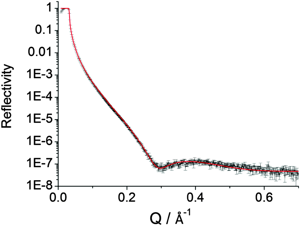 | ||
Fig. 2 Measured and refined ( ) XRR profiles for DEB films on p-type Si(100) surfaces. Reaction time was 120 min. The refined value of scattering length density28 is 11.8 × 10⁻⁶ Å−2 and comparable to those achieved for SAMs on gold substrates in close-packed Langmuir–Blodgett films.29 The XRR-determined film thickness is 1.1 nm which is close to the theoretical value of 0.9 nm (Chem3D). The symmetrical nature of DEB opens no routes to alternative surface binding modes. ) XRR profiles for DEB films on p-type Si(100) surfaces. Reaction time was 120 min. The refined value of scattering length density28 is 11.8 × 10⁻⁶ Å−2 and comparable to those achieved for SAMs on gold substrates in close-packed Langmuir–Blodgett films.29 The XRR-determined film thickness is 1.1 nm which is close to the theoretical value of 0.9 nm (Chem3D). The symmetrical nature of DEB opens no routes to alternative surface binding modes. | ||
The solvent and/or solute electron scavenging ability is expected to be important as it can influence electron–hole recombination events. Hence, solvents that reduce electron–hole recombination may favor the reaction of unsaturated nucleophilic molecules with surface-localized holes.6 It was therefore even more surprising to observe a total lack of reactivity when DEB grafting was attempted from a 5 mM solution in dichloromethane (DCM). DCM is a mild oxidizer (redox potential is −1.1 V vs. SCE in acetonitrile35) of low nucleophilicity and low dielectric constant (εDCM = 8.93). Halocarbons have good electron-accepting properties,36,37 and because the energy of a conduction band electron (ca. −3.5 eV) exceeds that of the solvent LUMO, the halocarbon solvent should be effective in trapping electrons, thus reducing recombination events6 and favoring reactions of surface holes with the nucleophilic DEB molecule.
The lack of reactivity of the DEB/DCM system (Fig. 1 and Fig. S1–S3, ESI†) would suggest that at room temperature, and without illumination of the Si sample, the electron-scavenging ability of the solvent alone does not suffice to bring about monolayer formation in the time scale of the experiment. A solvent like acetonitrile, a poor oxidizer (electron affinity, EA is ca. −2.84 eV)38 but with a high dielectric constant (εMeCN = 37.5), should afford an environment more favorable for electron transfer (ET), in this case putatively from the Si conduction band to the LUMO of DEB. Solvated electrons and solvent anions can coexist in liquid acetonitrile,39,40 and the higher dielectric constant could account, at-least to a degree (vide infra), for the appreciable rate-enhancing effect compared to halocarbon solvents. Electron affinity values, or rate constants for their reaction with hydrated electrons, are unfortunately not known for both DEB and for its close relative, phenylacetylene. A comparison with benzene would be of limited relevance as in this limit case the energy gain by adding an extra electron is exceedingly low (electron affinity for benzene is ca. −0.72 eV41 and the redox potential is as low as −3.4 V vs. SCE42). An interesting and relevant parallel can however be drawn with styrene. In this case it is possible to put forward a case for electron-trapping by this aromatic-conjugated olefin. The second-order rate constant for the trapping by styrene of hydrated electrons generated by pulsed radiolysis is 3.9 × 10¹⁰ M−1 s−1, a value higher than that of very good electron acceptors such as halogenated hydrocarbons (e.g. k = 3.0 × 10¹⁰ M−1 s−1 for both CCl4 and CHCl3).36 Butadiene, which lacks conjugation with an aromatic ring, is less able to scavenge hydrated electrons (k = 8.0 × 10⁹ M−1 s−1) while benzene, as well as ethylene, can be both classified as unreactive (k < 7.0 × 10⁶ M−1 s−1).36 We therefore tentatively suggest that electron-trapping by an aromatic-conjugated acetylene like DEB may limit electron–hole recombination events by scavenging hydrated electrons. As a result, a larger number of surface holes become available to initiate monolayer formation.
To add strength to this argument we replaced DEB by an aliphatic α,ω-dialkyne, 1,8-nonadiyne. As shown in Fig. 3 and Fig. S7 (ESI†) monolayer grafting of 1,8-nonadiyne is essentially undetectable over the time scale that suffices for the same reaction of DEB/acetonitrile to reach completion. In contrast to DEB, 1,8-nonadiyne lacks conjugation with a π-electron system and we suggest that its inertness toward Si–H under mild dark conditions lies mainly in the poor electron-trapping ability of this aliphatic hydrocarbon.
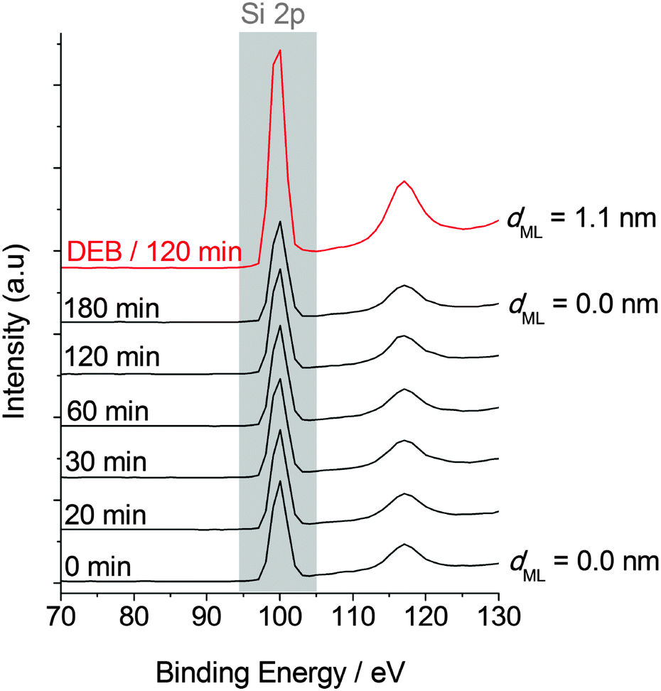 | ||
Fig. 3 Hydrosilylation of aromatic-conjugated alkynes and aliphatic alkynes; attenuation of the XPS substrate signal. Adsorbate is 5 mM 1,8-nonadiyne in MeCN, reactions are at room temperature in the dark. The invariance of the XPS Si 2p data over 180 min shows the lack of reactivity for aliphatic α,ω-diynes on n-type Si(100)–H. The mean free path (λSi,ML) of Si 2p electrons travelling across the organic film is set to 41.5 Å and the substrate signal should scale according to the law exp(−dML/λSi,ML). Estimated dML values are adjacent to the XPS trace. XPS data for the DEB/MeCN system ( ) are shown for comparison. ) are shown for comparison. | ||
There is however a number of other possible explanations we have considered. For example, the striking difference in reactivity between the DEB and 1,8-nonadiyne systems could be, in part, accounted for by the relative strength of cation–π interactions. Cation–π interactions are known to be significantly stronger in aromatic than in aliphatic compounds.43 In solution-phase systems, the solvent plays an important role toward the existence of silicon-based cations,44 and silylium ions (tricoordinate silicon atom, R3Si+)45 are known to form adducts with aromatic compounds stable enough for isolation.46,47 However, silylium ions are strong electrophilic centres,48,49 and a strong N-donor like acetonitrile in solution chemistry is rapidly silylated at nitrogen by silylium ions.50 This route would result in a silylnitrilium ion. In our XPS measurements we specifically looked for any silyl nitrilium species but the data for the DEB–acetonitrile system show no nitrogen signals (Fig. S4, ESI†). Our data, therefore, do not support this explanation.
We also considered a radical initiation step, possibly mediated by traces of oxygen,51 to account for the DEB high reactivity. The participation of oxygen would be in line with the solution-phase work of Zaborovskiy et al., who reported the spontaneous formation of silyl radicals by the reaction of tris(trimethylsilyl)silane (Me3Si)3Si–H with oxygen,52 and a parallel could also be made with the work of Chatgilialoglu et al., who observed that conjugation of the carbon–carbon triple bond with a π-system dramatically increases reaction rates for the radical hydrosilylation of 1-alkynes and 1-alkenes by molecular silanes.53 For example, rate constants for the addition at room temperature (ca. 300 K) of triethylsilyl radicals (Et3Si˙) to phenylacetylene (Ph–C![[triple bond, length as m-dash]](https://www.rsc.org/images/entities/char_e002.gif) CH), tert-butylacetylene (tBu–CCH), styrene (Ph–CH
CH), tert-butylacetylene (tBu–CCH), styrene (Ph–CH![[double bond, length as m-dash]](https://www.rsc.org/images/entities/char_e001.gif) CH2) and tert-butylethylene (tBu–CHCH2) are 1.0 × 10⁸ M−1 s−1, 2.3 × 10⁶, 2.2 × 10⁸ M−1 s−1 and 3.7 × 10⁶ M−1 s−1. However, it is difficult to reconcile our results in the presence of radical species; silyl radicals do react rapidly with unsaturated compounds,53 but they are also very efficient in abstracting chloride from alkyl halides.54 That is, the addition reaction is in competition with Cl abstraction, and therefore, in the case of a radical initiating step caused by molecular oxygen contaminations, chlorine should be present on surfaces prepared from DEB solutions in DCM. Chlorine-related emissions are absent in XPS spectra, evidence pointing to radical initiation as an unlikely event.55 We also note that other groups have cast doubt on oxygen playing the role of a radical initiator in hydrosilylation reactions.12,56
CH2) and tert-butylethylene (tBu–CHCH2) are 1.0 × 10⁸ M−1 s−1, 2.3 × 10⁶, 2.2 × 10⁸ M−1 s−1 and 3.7 × 10⁶ M−1 s−1. However, it is difficult to reconcile our results in the presence of radical species; silyl radicals do react rapidly with unsaturated compounds,53 but they are also very efficient in abstracting chloride from alkyl halides.54 That is, the addition reaction is in competition with Cl abstraction, and therefore, in the case of a radical initiating step caused by molecular oxygen contaminations, chlorine should be present on surfaces prepared from DEB solutions in DCM. Chlorine-related emissions are absent in XPS spectra, evidence pointing to radical initiation as an unlikely event.55 We also note that other groups have cast doubt on oxygen playing the role of a radical initiator in hydrosilylation reactions.12,56
It is very important to note that specific solvent–solute interactions may be more relevant in determining the efficiency of the electron-transfer (ET) than dielectric considerations on ET alone. For example, Mussell and Nocera reported cases of annihilation reactions where electron-transfer in DCM can occur at distances up to ∼12 Å and with efficiencies higher than those measured in a highly-coordinating solvent like acetonitrile.57 Computation data by Johnson and DiLabio suggest that on a quite hydrophobic surface like the Si(100)–2 × 1 the separation between a benzene molecule and the surface is possibly as small as 4 Å.17 Given the likelihood of close proximity between the aromatic adsorbate and the hydrogenated silicon surface, the greater reactivity of DEB in acetonitrile is unlikely to be exclusively related to the effect of the high dielectric on the ET reaction.
An additional and simple explanation accounting for these very mild hydrosilylation conditions would be that the solvent-assisted rate enhancement does not correlate explicitly with the solvent's dielectric constant but parallels the dipole moment and acid–base character of the solvent. With porous silicon (PSi), solvents with a large dipole moment may attract holes and electrons to the surface,58 with both nitrogen- and oxygen-containing solvents then efficiently trapping surface holes and quenching the PSi photoluminescence.59 To probe the relative effect of the solvent dielectric constant versus its dipole moment and acid–base character, experiments were run with THF as the DEB solvent. THF and DCM are very close in terms of dielectric constant and polarity (ε = 7.58, μTHF = 1.75, μDCM = 1.55), but in sharp contrast to DCM, as a result of Lewis acid–base stabilization of surface traps, THF can significantly reduce the rate of radiative recombination for h+–e− pairs. In this case the h+–e− pair that does not radiatively recombine can be separated by the electric field in the space-charge region, with holes surviving long enough to become susceptible to nucleophilic attack. The hydrosilylation of a nucleophile like DEB on dark Si(100)–H surfaces with THF as the solvent, as for the DCM system, was also unsuccessful (Fig. 1a and Fig. S8, ESI†). A significant role of the solvent's dipole moment and acid–base character in the stabilization of surface holes is, therefore, not in-line with our data.
Monolayer formation initiated by nucleophilic attack of surface holes, as for illuminated Si samples,8,60 appears therefore difficult to reconcile with our contrasting acetonitrile/THF results in the dark. The mechanistic picture gets clearer when considering the work of Fellah et al., who argued in favor of the solvent dielectric having a key role in defining the rate of h+/e− recombination in PSi.61,62 In the case of a solvent-impregnated PSi matrix, solvents with a large dielectric constant have the greatest quenching effect on radiative h+/e− recombination; this can be explained in terms of solvent-induced dielectric screening that limits the Onsager length (i.e., the h+/e− distance at which Coulomb attractions equal kT). This effect reaches saturation at a dielectric value of approximately 20, with acetonitrile expected to have a stronger quenching effect on photoluminescence than DCM or THF.61 The speed of monolayer formation in the acetonitrile system therefore suggests that screening of Coulomb attraction between holes and electrons do play an important role under mild dark conditions.
It therefore seems unlikely that the solvent electron scavenging and/or dielectric factors on the ET between the active adsorbate and the substrate alone can govern the hydrosilylation rate by Si(100)–H at room temperature and in the dark. Under these very mild conditions it appears that the interplay between stabilization of surface traps and the electron-accepting properties of the adsorbate plays a more important role. If these factors are addressed, as shown in Fig. 1, the reaction progresses only marginally more rapidly in n-type Si, but it is still rather efficient on the p-type counterpart.63
The mechanistic study above shows that monolayers can be formed on Si–H surfaces quickly without light excitation and from dilute systems of aromatic unactivated 1-alkynes. This is a mild strategy for the modification of n- and p-doped silicon by an organic layer, a capability of enormous technological interest.3 In this case we demonstrate the further utility of this chemistry by further functionalising the DEB-modified silicon surface.4 This is possible as the monolayer derived from DEB leaves a distal alkyne moiety, which is an excellent target for tagging with organic azide through the archetypal “click” reaction, the copper-catalyzed alkyne–azide cycloaddition (CuAAC).19,21,27,64
The electronic properties of the silicon substrate are easily tuned and a wealth of processes is available for the micro- and nano-patterning of this material; both these factors have been behind a remarkable research effort in trying to integrate redox-active molecules onto silicon electrodes.65 Ferrocene derivatives exhibit attractive electrochemical characteristics,66–68 and azidomethylferrocene20 was chosen here to demonstrate the functionalization of the DEB-passivated p-type Si(100) electrode. The ferrocene molecule has the dual role of (i) affording an insight into the charge transfer across the organic film as well as (ii) greatly simplifying the analytical task of assessing the outcome of CuAAC “click” reactions at the electrode surface (Scheme 1). Beginning with the latter, the Fe 2p3/2 and Fe 2p1/2 peaks, clearly visible at 708.4 and 721.4 eV in the high-resolution XPS spectrum (Fig. 4a), are consistent with values reported in the literature,68,69 and support the formation of the ferrocene layer. From the comparison of XPS- and stoichiometrically-derived Fe:N and N:(C–O/–N)70 atomic ratios it is possible to infer that the molecular nature of the ferrocene molecule is not appreciably altered upon its immobilization. C 1s and N 1s XPS data19 (Fig. 4c and d) agree with the conversion of surface acetylene moieties to the putative surface CuAAC product, and the approximate fractional monolayer coverage of SiOx varied from not detectable (<0.06) to ca. 0.2 monolayer equivalents (Fig. 4d). The presence of silicon oxide signals in the 102–104 eV region of the XPS spectra is indicative of passivation of the semiconductor surface that is inferior to the one that can be achieved by thermal reactions of aliphatic α,ω-dialkynes.21 It is noteworthy, however, that despite the presence of silica contaminations the redox films exhibited remarkably stable cyclic voltammetric peaks,71 attributable to the ferrocene/ferricenium surface reaction, and surface coverage values, Γ, that ranged from ca. 1.8 × 10⁻¹¹ to ca. 2.5 × 10⁻¹¹ mol cm−2 (Fig. 5a). This coverage is in the range 40–56% of that expected for a hexagonally close-packed full monolayer of ferrocene molecules, assuming the molecule to be spherical with a diameter of 0.66 nm.66
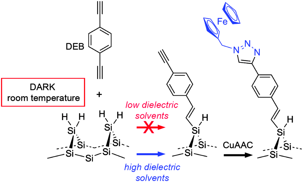 | ||
| Scheme 1 Dark hydrosilylation of an aromatic-conjugated acetylene (DEB) at room temperature and CuAAC “click” derivatization of the functional monolayer. | ||
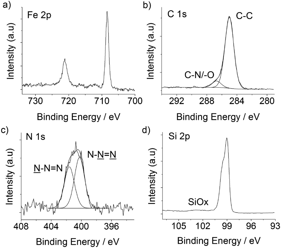 | ||
| Fig. 4 High resolution XPS scans for CuAAC modified DEB samples. | ||
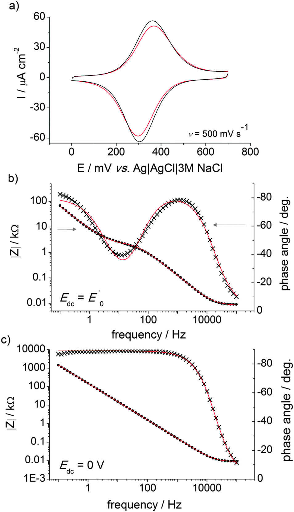 | ||
Fig. 5 Representative CVs (a, cycle n. 1 and cycle n. 100) and EIS and Bode plots (b and c) for ferrocene-modified DEB samples at either an applied potential Edc = E0′ or Edc = 0 V. The frequency range was from 100 kHz to 100 mHz. All symbols are experimental data and solid lines are best fits to the data (χ2 < 0.004). The rate constant for the electron transfer,  , was 9.4 s−1 (Rs = 8.4 Ω, Cdl = 2.25 μF (ϕ = 0.94), Cads = 21.5 μF (ϕ = 0.89), Rct = 2486 Ω, the electrode area was 0.28 cm−2). , was 9.4 s−1 (Rs = 8.4 Ω, Cdl = 2.25 μF (ϕ = 0.94), Cads = 21.5 μF (ϕ = 0.89), Rct = 2486 Ω, the electrode area was 0.28 cm−2). | ||
Modular schemes offer considerable synthetic versatility but at the risk of multi-step chemistry leading to reduction of the electronic coupling between the redox element and the substrate. For this reason we measured the kinetics of the electrochemically-initiated ET between the electrode and the ferrocene moiety using electrochemical impedance spectroscopy (EIS).72Fig. 5b shows the Bode representations of the impedance data at either Edc ∼ E0′ in Fig. 5b or at Edc ∼ 0 V vs. reference in Fig. 5c (Edc, dc offset). For strongly adsorbed electroactive species the relationship between the circuit elements (Cdl, double-layer capacitance; Cads, adsorption pseudo-capacitance; Rct, charge transfer resistance)73 of and the kinetic parameters characterizing a redox system has been described in the literature.74–78 Using the refined Rct and Cads values, we obtained a  value of 8 ± 2 s−1. This value indicates ET kinetics that are comparable to that of aliphatic films20 of comparable length.79
At a sufficiently cathodic applied dc potential (Edc = 0 V, Fig. 5c), the phase angle of the Bode plots adopts a sigmoidal shape that starts near 0° at high frequency and shifts close to 90° at frequencies of <100 Hz. An ideal series RC circuit would have the lower-frequency points at 90° because the response is dominated by the double-layer capacitance charging. The EIS data thus suggest a blocking or insulating monolayer that can be modelled using a circuit that does not model a charge-transfer reaction but describes a polarizing electrode77 (i.e. with two terms Rs and Cdl in series).80
Conclusions
Our experimental observations point to a strategy to overcome the generally higher reactivity of n-type semiconductor Si surfaces toward attack by nucleophilic adsorbates, and expand the available repertoire of mild wet chemistry routes to functional surfaces.All non-oxide semiconductors are susceptible to anodic degradation and the DEB passivation of the Si(100) electrode as achieved by dark and room temperature hydrosilylation reactions remains poor when compared to alternative grafting methods.3 However, we believe the exceedingly mild monolayer-forming conditions reported in this paper are remarkable and will stimulate further experimental scrutiny. Notably, films incorporating phenyl rings and bi-functional contacts also hold considerable advantages when making top contacts in molecular devices.81
Notes and references
- J. M. Buriak, Chem. Commun., 1999, 1051 RSC.
- A. Vilan, O. Yaffe, A. Biller, A. Salomon, A. Kahn and D. Cahen, Adv. Mater., 2010, 22, 140 CrossRef CAS PubMed.
- S. Ciampi, J. B. Harper and J. J. Gooding, Chem. Soc. Rev., 2010, 39, 2158 RSC.
- J. J. Gooding and S. Ciampi, Chem. Soc. Rev., 2011, 40, 2704 RSC.
- S. Fellah, R. Boukherroub, F. Ozanam and J.-N. Chazalviel, Langmuir, 2004, 20, 6359 CrossRef CAS PubMed.
- L. A. Huck and J. M. Buriak, J. Am. Chem. Soc., 2012, 134, 489 CrossRef CAS PubMed.
- B. Rijksen, B. van Lagen and H. Zuilhof, J. Am. Chem. Soc., 2011, 133, 4998 CrossRef CAS PubMed.
- L. A. Huck and J. M. Buriak, Langmuir, 2012, 28, 16285 CrossRef CAS PubMed.
- T. K. Mischki, G. P. Lopinski and D. D. M. Wayner, Langmuir, 2009, 25, 5626 CrossRef CAS PubMed.
- M. V. Lee, J. R. I. Lee and T. M. Willey, Jpn. J. Appl. Phys., 2011, 50, 01BD01 CrossRef.
- X. Wang, R. E. Ruther, J. A. Streifer and R. J. Hamers, J. Am. Chem. Soc., 2010, 132, 4048 CrossRef CAS PubMed.
- M. V. Lee, R. Scipioni, M. Boero, P. L. Silvestrelli and K. Ariga, Phys. Chem. Chem. Phys., 2011, 13, 4862 RSC.
- R. Zanoni, Sci. Adv. Mater., 2011, 3, 378 CrossRef CAS.
- A. Ng, S. Ciampi, M. James, J. B. Harper and J. J. Gooding, Langmuir, 2009, 25, 13934 CrossRef CAS PubMed.
- L. Scheres, M. Giesbers and H. Zuilhof, Langmuir, 2010, 26, 4790 CrossRef CAS PubMed.
- H. Sano, M. Zhao, D. Kasahara, K. Murase, T. Ichii and H. Sugimura, J. Colloid Interface Sci., 2011, 361, 259 CrossRef CAS PubMed.
- E. R. Johnson and G. A. DiLabio, J. Phys. Chem. C, 2009, 113, 5681 CAS.
- L. Scheres, A. Arafat and H. Zuilhof, Langmuir, 2007, 23, 8343 CrossRef CAS PubMed.
- S. Ciampi, G. Le Saux, J. B. Harper and J. J. Gooding, Electroanalysis, 2008, 20, 1513 CrossRef CAS.
- S. Ciampi, P. K. Eggers, G. Le Saux, M. James, J. B. Harper and J. J. Gooding, Langmuir, 2009, 25, 2530 CrossRef CAS PubMed.
- S. Ciampi, T. Böcking, K. A. Kilian, M. James, J. B. Harper and J. J. Gooding, Langmuir, 2007, 23, 9320 CrossRef CAS PubMed.
- L. J. Webb and N. S. Lewis, J. Phys. Chem. B, 2003, 107, 5404 CrossRef CAS.
- A. Nelson, J. Appl. Crystallogr., 2006, 39, 273 CrossRef CAS.
- E. Laviron, J. Electroanal. Chem., 1979, 97, 135 CrossRef CAS.
- P. Allongue, C. Henry de Villeneuve, S. Morin, R. Boukherroub and D. D. M. Wayner, Electrochim. Acta, 2000, 45, 4591 CrossRef CAS.
- Y. J. Chabal, G. S. Higashi, K. Raghavachari and V. A. Burrows, J. Vac. Sci. Technol., A, 1989, 7, 2104 CAS.
- M. Meldal and C. W. Tornøe, Chem. Rev., 2008, 108, 2952 CrossRef CAS PubMed.
- Y. González-García, J. M. C. Mol, T. Muselle, I. De Graeve, G. Van Assche, G. Scheltjens, B. Van Mele and H. Terryn, Electrochem. Commun., 2011, 13, 169 CrossRef.
- A. Ulman, An Introduction to Ultrathin Organic Films, Academic Press, 1991 Search PubMed.
- The attenuation of the silicon signal scales according to the law exp(−dML/λSi,ML) and it can be used to estimate the film thickness after the grafting of DEB molecules: dML/λSi,ML(1cosθ) = −ln(Si 2pML/Si 2pclean), where Si 2pML is the integrated area of the Si 2p peak, Si 2pclean is the Si 2p peak area of an unmodified and clean Si substrate, dML is the thickness of the grafted organic layer, λSi,ML is the mean free path of Si 2p electrons travelling across the organic film (41.5 Å), and θ is the photoelectron take-off angle with respect to the surface normal.
- Semi-empirical calculations with Chem3D.
- R. L. Cicero, M. R. Linford and C. E. D. Chidsey, Langmuir, 2000, 16, 5688 CrossRef CAS.
- See the ESI† paragraph for a detailed discussion of the model.
- M. Kondo, T. E. Mates, D. A. Fischer, F. Wudl and E. J. Kramer, Langmuir, 2010, 26, 17000 CrossRef CAS PubMed.
- A. A. Isse, C. Y. Lin, M. L. Coote and A. Gennaro, J. Phys. Chem. B, 2010, 115, 678 CrossRef PubMed.
- E. J. Hart, S. Gordon and J. K. Thomas, J. Phys. Chem., 1964, 68, 1271 CrossRef CAS.
- I. P. Bell, M. A. J. Rodgers and H. D. Burrows, J. Chem. Soc., Faraday Trans. 1, 1977, 73, 315 RSC.
- K. D. Jordan and P. D. Burrow, Acc. Chem. Res., 1978, 11, 341 CrossRef CAS.
- C. Xia, J. Peon and B. Kohler, J. Chem. Phys., 2002, 117, 8855 CrossRef CAS.
- I. A. Shkrob and M. C. Sauer, J. Phys. Chem. A, 2002, 106, 9120 CrossRef CAS.
- R. S. Ruoff, K. M. Kadish, P. Boulas and E. C. M. Chen, J. Phys. Chem., 1995, 99, 8843 CrossRef CAS.
- J. Mortensen and J. Heinze, Angew. Chem., Int. Ed. Engl., 1984, 23, 84 CrossRef.
- J. W. Caldwell and P. A. Kollman, J. Am. Chem. Soc., 1995, 117, 4177 CrossRef CAS.
- M. Chauhan, C. Chuit, R. J. P. Corriu and C. Reyé, Tetrahedron Lett., 1996, 37, 845 CrossRef CAS.
- C. A. Reed, Acc. Chem. Res., 2009, 43, 121 CrossRef PubMed.
- M. F. Ibad, P. Langer, A. Schulz and A. Villinger, J. Am. Chem. Soc., 2011, 133, 21016 CrossRef CAS PubMed.
- T. Nishinaga, Y. Izukawa and K. Komatsu, Tetrahedron, 2001, 57, 3645 CrossRef CAS.
- M. Kira, T. Hino and H. Sakurai, J. Am. Chem. Soc., 1992, 114, 6697 CrossRef CAS.
- C. Douvris, E. S. Stoyanov, F. S. Tham and C. A. Reed, Chem. Commun., 2007, 1145 RSC.
- G. A. Olah, G. Rasul and G. K. S. Prakash, J. Am. Chem. Soc., 1999, 121, 9615 CrossRef CAS.
- Previous works have suggested a radical initiation, mediated by traces of oxygen, for the dark hydrosilylation of activated 1-alkynes at room temperature see Y. Liu, S. Yamazaki, S. Yamabe and Y. Nakato, J. Mater. Chem., 2005, 15, 4906–4913 RSC.
- A. B. Zaborovskiy, D. S. Lutsyk, R. E. Prystansky, V. I. Kopylets, V. I. Timokhin and C. Chatgilialoglu, J. Organomet. Chem., 2004, 689, 2912 CrossRef CAS.
- C. Chatgilialoglu, K. U. Ingold and J. C. Scaiano, J. Am. Chem. Soc., 1983, 105, 3292 CrossRef CAS.
- C. Chatgilialoglu, K. U. Ingold and J. C. Scaiano, J. Am. Chem. Soc., 1982, 104, 5123 CrossRef CAS.
- Cl 2p and 2s peaks are at ca. 200 and ca. 270 eV, binding energy, see L. J. Webb, E. J. Nemanick, J. S. Biteen, D. W. Knapp, D. J. Michalak, M. C. Traub, A. S. Y. Chan, B. S. Brunschwig and N. S Lewis, J. Phys. Chem. B, 2005, 109, 3930–3937 CrossRef CAS PubMed.
- M. Woods, S. Carlsson, Q. Hong, S. N. Patole, L. H. Lie, A. Houlton and B. R. Horrocks, J. Phys. Chem. B, 2005, 109, 24035 CrossRef CAS PubMed.
- R. D. Mussell and D. G. Nocera, J. Phys. Chem., 1991, 95, 6919 CrossRef CAS.
- J. M. Lauerhaas, G. M. Credo, J. L. Heinrich and M. J. Sailor, J. Am. Chem. Soc., 1992, 114, 1911 CrossRef CAS.
- W. Jun Jin, G. Li Shen and R. Qin Yu, Spectrochim. Acta, Part A, 1998, 54, 1407 CrossRef.
- L. A. Huck and J. M. Buriak, J. Am. Chem. Soc., 2011, 134, 489 CrossRef PubMed.
- S. Fellah, R. B. Wehrspohn, N. Gabouze, F. Ozanam and J. N. Chazalviel, J. Lumin., 1999, 80, 109 CrossRef.
- S. Fellah, F. Ozanam, N. Gabouze and J. N. Chazalviel, Phys. Status Solidi A, 2000, 182, 367 CrossRef CAS.
- As the Si wafer is in contact with a non-conductive solution and it is therefore difficult to estimate the semiconductor band-bending.
- S. Ciampi, T. Böcking, K. A. Kilian, J. B. Harper and J. J. Gooding, Langmuir, 2008, 24, 5888 CrossRef CAS PubMed.
- B. Fabre, Acc. Chem. Res., 2010, 43, 1509 CrossRef CAS PubMed.
- G. K. Rowe and S. E. Creager, Langmuir, 1991, 7, 2307 CrossRef CAS.
- P. K. Eggers, N. Darwish, M. N. Paddon-Row and J. J. Gooding, J. Am. Chem. Soc., 2012, 134, 7539 CrossRef CAS PubMed.
- K. M. Roth, A. A. Yasseri, Z. Liu, R. B. Dabke, V. Malinovskii, K.-H. Schweikart, L. Yu, H. Tiznado, F. Zaera, J. S. Lindsey, W. G. Kuhr and D. F. Bocian, J. Am. Chem. Soc., 2003, 125, 505 CrossRef CAS PubMed.
- C. M. Woodbridge, D. L. Pugmire, R. C. Johnson, N. M. Boag and M. A. Langell, J. Phys. Chem. B, 2000, 104, 3085 CrossRef CAS.
- Sum of photoemissions from nitrogen- and oxygen-bonded carbons. A discussion on the origin of the oxygen-bound carbons for the reactions of acetylenes and hydrogenated silicon surfaces is found in ref. 34.
- In aqueous environments the decrease in Γ values was less than 8% after 100 CV cycles (Fig. 5a).
- E. Laviron, J. Electroanal. Chem., 1979, 105, 35 CrossRef CAS.
- Both Cdl and Cads showed a frequency-dependent capacitive behavior and were therefore treated as constant-phase elements (CPEs), a mathematical formalism used to model an imperfect capacitor in an electrical circuit. For a CPE the impedance is equal to 1/Q (jω)−φ, in which ω is the angular frequency, Q is a parameter with the units of V−1 cm−2 s, and φ is an exponential term with values between 0 and 1. CPE defines inhomogeneity in the electrochemical system.
- S. Song, R. A. Clark, E. F. Bowden and M. J. Tarlov, J. Phys. Chem., 1993, 97, 6564 CrossRef CAS.
- S. E. Creager and T. T. Wooster, Anal. Chem., 1998, 70, 4257 CrossRef CAS.
- J. Liu, Y. Jin, A. Wu, Z. Li and S. Dong, Electroanalysis, 2004, 16, 1931 CrossRef CAS.
- A. D. Abhayawardhana and T. C. Sutherland, J. Phys. Chem. C, 2009, 113, 4915 CAS.
- S. Ciampi, M. James, N. Darwish, E. Luais, B. Guan, J. B. Harper and J. J. Gooding, Phys. Chem. Chem. Phys., 2011, 13, 15624 RSC.
- It is important to note that attempts to compare rates constants for the electron-transfer of chemically distinct redox constructs is not trivial and has to take into account several factors. For example, variations in electrode kinetics may be associated with (i) the length and nature of the electron-transfer bridge and with the properties/concentration of the any diluent molecule in the SAM see P. K. Eggers, D. B. Hibbert, M. N. Paddon-Row and J. J. Gooding, J. Phys. Chem. C, 2009, 113, 8964–8971 Search PubMed , and (ii) with either space-charge effects at the monolayer/solvent interface or changes in adsorption geometry induced by SAM dilution/concentration or both, see K. M. Roth, A. A. Yasseri, Z. Liu, R. B. Dabke, V. Malinovskii, K.-H. Schweikart, L. Yu, H. Tiznado, F. Zaera, J. S. Lindsey, W. G. Kuhr and D. F. Bocian, J. Am. Chem. Soc., 2003, 125, 505–517 CrossRef CAS PubMed.
- Curve fitting results in an interfacial capacity, Cdl, of ca. 3.8 μF cm−2 (φ = 0.99). The value of Helmholtz capacitance for both hydrogen-terminated and monolayer-modified silicon electrodes is generally found to be lower than for metal electrodes E. J. Faber, W. Sparreboom, W. Groeneveld, L. C. P. M. de Smet, J. Bomer, W. Olthuis, H. Zuilhof, E. J. R. Sudhölter, P. Bergveld and A. van den Berg, pH Sensitivity of Si-C Linked Organic Monolayers on Crystalline Silicon Surfaces, ChemPhysChem, 2007, 8, 101–112 CrossRef CAS PubMed.
- R. T. W. Popoff, A. A. Zavareh, K. L. Kavanagh and H.-Z. Yu, J. Phys. Chem. C, 2012, 116, 17040 CAS.
Footnotes |
| † Electronic supplementary information (ESI) available: Additional XPS, XRR and spectroscopic ellipsometry data. See DOI: 10.1039/c4cp00396a |
| ‡ Current address: Intelligent Polymer Research Institute, AIIM Facility, University of Wollongong, Wollongong, NSW 2522, Australia. |
| § Current address: Université François Rabelais de Tours, CNRS, CEA, ENIVL, GREMAN UMR 7347, Tours, France. |
| This journal is © the Owner Societies 2014 |