 Open Access Article
 This Open Access Article is licensed under a
 Creative Commons Attribution 3.0 Unported Licence
The fabrication, characterisation and electrochemical investigation of screen-printed graphene electrodes†
Edward P.
Randviir
,
Dale A. C.
Brownson
,
Jonathan P.
Metters
,
Rashid O.
Kadara
and
Craig E.
Banks
*
Faculty of Science and Engineering, School of Science and the Environment, Division of Chemistry and Environmental Science, Manchester Metropolitan University, Chester Street, Manchester M1 5GD, Lancs, UK. E-mail: c.banks@mmu.ac.uk; Web: www.craigbanksresearch.com Fax: +44 (0)1612476831; Tel: +44 (0)1612471196
First published on 24th January 2014
Abstract
We report the fabrication, characterisation (SEM, Raman spectroscopy, XPS and ATR) and electrochemical implementation of novel screen-printed graphene electrodes. Electrochemical characterisation of the fabricated graphene electrodes is undertaken using an array of electroactive redox probes and biologically relevant analytes, namely: potassium ferrocyanide(II), hexaammine-ruthenium(III) chloride, N,N,N′,N′-tetramethyl-p-phenylenediamine (TMPD), β-nicotinamide adenine dinucleotide (NADH), L-ascorbic acid (AA), uric acid (UA) and dopamine hydrochloride (DA). The electroanalytical capabilities of the fabricated electrodes are also considered towards the sensing of AA and DA. The electrochemical and (electro)analytical performances of the fabricated screen-printed graphene electrodes are considered with respect to the relative surface morphologies and material compositions (elucidated via SEM, Raman, XPS and ATR spectroscopy), the density of electronic states (% global coverage of edge-plane like sites/defects) and the specific fabrication conditions utilised. Comparisons are made between two screen-printed graphene electrodes and alternative graphite based screen-printed electrodes. The graphene electrodes are fabricated utilising two different commercially prepared ‘graphene’ inks, which have long screen ink lifetimes (>3 hours), thus this is the first report of a true mass-reproducible screen-printable graphene ink. Through employment of appropriate controls/comparisons we are able to report a critical assessment of these screen-printed graphene electrodes. This work is of high importance and demonstrates a proof-of-concept approach to screen-printed graphene electrodes that are highly reproducible, paving the way for mass-producible graphene sensing platforms in the future.
Introduction
Graphene is a two dimensional hexagonal carbon structure arranged from sp2 hybridised carbon atoms which has attracted growing and continued interest from scientists due to its reported unique properties,1 such as its high mechanical strength and electrical conductivity.2,3 Intensive research into the utilisation of graphene's reported outstanding properties has the potential to create both novel and enhanced technologies.4 The realisation of such potential is beginning to emerge, with graphene based devices reportedly innovating numerous fields when employed, for example in transistors,5 transducers,6 chemical sensors,7 DNA sequencing,8 solar cells,9 batteries,10 capacitors11 and rust prevention.12 The apparent graphene ‘gold rush’ has originated from such reports,4 where improved device performances have proven the concept of beneficial graphene employment for a multitude of applications.13 Consequently, attention has now turned to fully exploring graphene's commercial potential, which, as one has come to expect with graphene, is a source of great excitement and expectation.One area that has completely embraced the graphene revolution is the electrochemical utilisation of graphene-based electrode substrates.14 Graphene is potentially the world's thinnest electrode material, with numerous reports detailing the beneficial implementation of graphene in electrochemistry, for example in the fabrication of enhanced electroanalytical sensors and in a multitude of energy generation and storage devices.15–18 The aforementioned reports demonstrate that, in certain cases, graphene can provide electrocatalysis for an improved analytical performance and/or improved direct electron transfer at the graphene|electrolyte interface when used as components for improved analytical/energy based devices (relative to existing electrode materials).15–18 However, although there are many optimistic reports concerning the electrochemical benefits of graphene, contrasting reports exist which demonstrate that this is not always the case.19,20
In terms of employing graphene as an electrode material, a major problem that researchers face is electrically ‘wiring’ the graphene in order for electrons to flow efficiently, thus allowing one to observe the electrochemical benefits from the graphene structure.14 The most widely used approach to study graphene (on the macroscopic scale) is drop-casting aliquots of a graphene suspension onto an underlying supporting electrode surface, such that one immobilises graphene and effectively averages the total response over that of the graphene domains.14,21 However, modifying such surfaces has potential to leave underlying ‘reactive’ surfaces exposed, which can influence and (in specific cases) dominate the observed electrochemistry.14,19 Furthermore, capillary forces present as a result of solvent evaporation can push graphene platelets to the edges of the underlying electrode (see Fig. 1) which can potentially leave concentrated zones of graphene at the edges of the electrode surface in addition to areas where there is little or no graphene coverage, which is akin to the so-called coffee ring effect; Fig. 1 shows a schematic overview of this process. The resultant uneven graphene distribution effectively leaves areas of both fast (multilayer graphene) and slow (single layer graphene) electron transfer and thus an electrochemically heterogeneous surface.
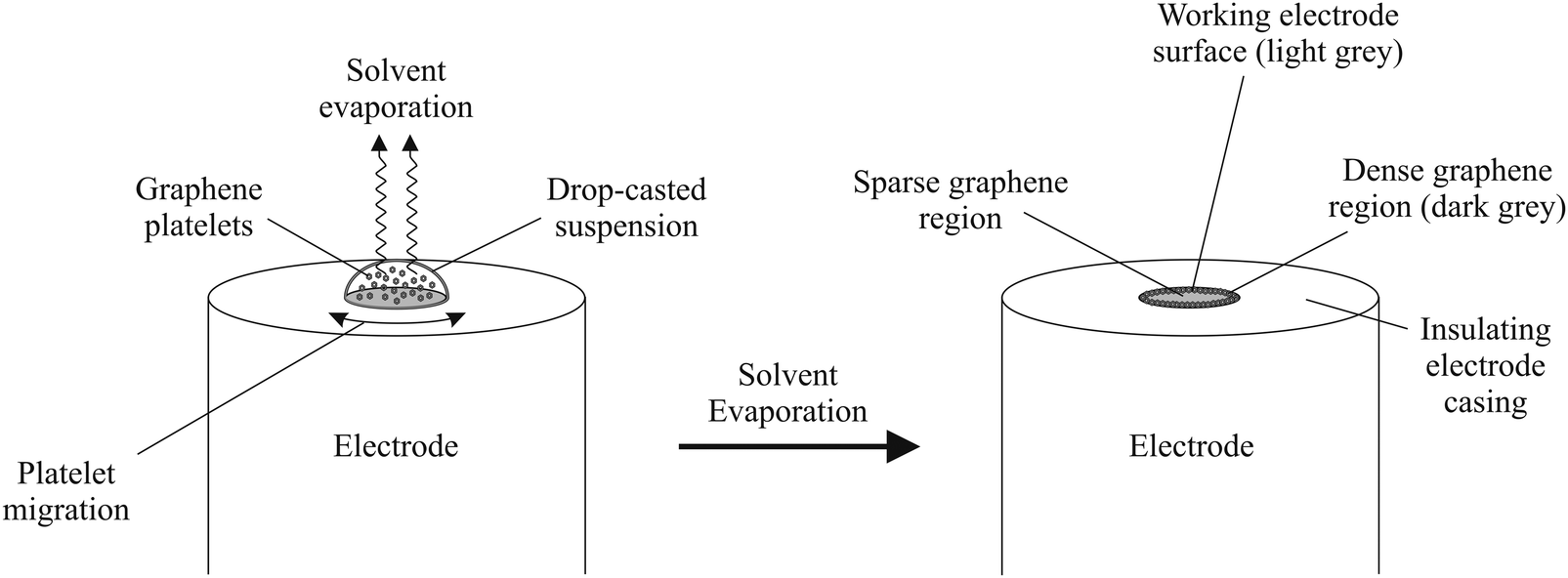 | ||
| Fig. 1 Typical coverage of graphene resulting from drop-casting a dispersion of the graphene of interest (suspended in a suitable solvent) onto a supporting electrode surface. Such an approach is extensively utilised within the academic literature in order to ‘connect to’ and electrically wire the graphene. | ||
To try and overcome the aforementioned issues, researchers have turned to exploring the electrochemistry of graphene through the utilisation of CVD grown graphene.22 Due to the nature of the CVD process, pristine monolayer graphene domains can be grown and transferred onto electrochemically inert substrates such that one can study the fundamental electrochemical properties whilst controlling the thickness of graphene and performing in situ characterisation of their electrode material – overcoming the earlier noted issues once one connects to the graphene.14,22,23 It is important to note however, that in cases where CVD grown graphene is utilised, the more commonly encountered CVD substrates are nickel and copper,22,24 which can interfere with the observed electrochemistry either beneficially or detrimentally (such as masking the electrochemical processes taking place at the graphene surfaces) if the graphene is not sufficiently transferred post-synthesis onto an electrochemically inert alternative substrate.22,25,26 Notably, graphene of similar quality and controllability to that obtained via the CVD process can be produced to study its electrochemical properties utilising the original graphene isolation method of mechanically exfoliating layers from HOPG and subsequently applying the residue onto a silicon dioxide slide.17,27 This method has been investigated by Valota et al.,27 who were successful in electrochemically characterising a graphene working electrode. Although the above noted methods are able to overcome the limitations of connecting to and studying the fundamental electrochemistry of graphene, they prove cumbersome if one wishes to mass produce graphene electrode substrates and indeed fabricate reproducible graphene electrodes, i.e. such as that required for the potential commercialisation of graphene-based devices/sensors.
Screen-printed electrodes (SPEs) have attracted a considerable degree of attention in recent years, particularly in terms of their application in electroanalysis.28–30 Disposable SPEs generally offer beneficial attributes over the more traditional electrodes, given that they are portable and cost-effective with their manufacturing process ultimately facilitating the rapid and facile mass production of reproducible sensors which offer true potential for application in-the-field.28 As such there is wide potential scope for the implementation of mass producible graphene based screen-printed electrochemical sensors in areas such as medicine, food and environmental science.14,28 However, given the known benefits and widespread electrochemical exploration of both graphene and SPEs alike, reports concerning the fabrication and use of disposable graphene-based-SPEs are surprisingly limited. The most commonly encountered method of utilising SPEs for graphene exploration in electrochemistry involves the drop-casting modification of existing carbon black-based or graphite-based SPEs with graphenes, of which there are numerous examples; see for instance ref. 31–37. However, such examples fall foul of the earlier noted issues that arise when employing this modification method (the process of physically immobilising graphene upon an underlying electrode support) and furthermore, the sensitivity and reproducibility of these electrodes is resultantly extremely poor, with the modification step resulting in a complex fabrication process. To overcome such issues, the fabrication of graphene SPEs through the incorporation of graphene into the printable inks (rather than graphite and/or carbon black alternatives) is the most plausible approach. Currently, to the best of our knowledge, there is only one such example that has utilised a graphene-based screen-printing ink to fabricate a SPE.38 In said work, Ping et al. demonstrate the fabrication and characterisation of a graphene SPE utilising an in-house synthesised graphene ink towards the beneficial ‘electrocatalytic’ detection of ascorbic acid (AA), dopamine (DA) and uric acid (UA) in real samples.38 However, the graphene utilised in their study was fabricated through the reduction of graphitic oxide (created via the modified Hummers method) and thus the reported ‘electrocatalytic’ effects most likely result from the presence of a large number of edge plane-like sites/defects present on the basal plane of the graphene surface (which is an inherent property of graphene produced in this manner and would not be present if using pristine graphene)14,20 and likely has a contribution from metal ions impregnated into the graphene structures (originating from the strong acids utilised in the graphene synthesis). As such, one can infer that the fabricated SPE is electrochemically more graphite-like than graphene-like in nature with respect to the reported edge plane content.14,39 Additionally, the developed ink was not a true screen-printable ink, defined as an ink that can be used on a screen for many hours (typically a screen life of >2 or 3 hours). Furthermore, although control experiments were performed with graphite-based alternative SPEs, the presence of oxygenated species (remaining from the incomplete reduction of graphitic oxide to graphene) have been shown to significantly contribute to the observed electrochemistry, and as such a key control/comparison experiment utilising a graphene oxide-based SPE is missing from this work in order to determine the origin of the reported ‘electrocatalytic’ response.14,20 Through further critical analysis of this work, it must be noted that Raman spectra of the graphene ink utilised and the resultant graphene SPEs were not provided, thus there was no evidence to indicate the presence of single-layer graphene.38 Rather, the surface topography of their graphene-SPE was examined via Atomic Force Microscopy (AFM) and SEM imaging and indicated an abundance of graphitic islands present instead of a uniform graphene (basal plane orientated) coverage;38 it is thus no surprise that the fabricated electrode exhibits edge plane-like voltammetry given its composition deviates from that expected for true graphene.25,26
Given the insights gained from the former literature example,38 it appears that the fabrication of graphene-based SPEs is plausible, however, given that the graphene SPE in this example is likely highly functionalised and possesses a large (graphite-like) edge plane content due to the defect-abundant graphene utilised, to the best of our knowledge, there is no present example detailing the fabrication and implementation of a true graphene-like SPE.
In this paper we report the fabrication, characterisation and electrochemical utilisation of what we believe to be the first real Graphene Screen-Printed Electrodes (GSPEs), which are fully characterised (via SEM, Raman, XPS and ATR spectroscopy) prior to experimental use. This work utilises ‘newly commercially available’ printable graphene inks from reputable screen-printing companies rather than lab-synthesised graphene inks. Comparisons of the electrochemical properties/performances are made between the two different ‘graphene’ inks utilised to fabricate the screen-printed graphene electrodes, with further control experiments employed with respect to comparing the graphene-SPEs to alternative graphite based SPEs;20 thus the ‘graphene’ electrodes are critically explored relative to the benefits of graphene implementation for the fabrication of commercially viable and disposable screen-printable electrodes. This work provides insight into the electrochemical properties of both graphene and graphite based SPEs, detailing a new perspective into the future design and fabrication of such SPEs with distinct electrode properties realised which results in possible enhancements for future graphene based ‘tailored’ screen-printing technology.
Experimental section
All chemicals were of the highest grade available and were used as received (without further purification) from Sigma Aldrich (UK). All solutions were prepared using deionised water of resistivity no less than 18.2 MΩ cm and were vigorously degassed prior to electrochemical measurements with high purity, oxygen free nitrogen. All test solutions (containing the electrochemical redox probes and biological analytes of relevance) were prepared in 0.1 M (pH 7.4) Phosphate Buffer Solution (PBS) containing 0.1 M KCl supporting electrolyte.Electrochemical measurements were performed using an Ivium Compactstat™ (Netherlands) potentiostat. All measurements were conducted using a screen-printed three electrode system as described below. For SEM, Raman, XPS and ATR spectroscopy the respective inks or screen-printed electrodes were used as received/fabricated without any further modification. Scanning electron microscope (SEM) images and surface element analysis were obtained with a JEOL JSM-5600LV model equipped with an energy-dispersive X-ray microanalysis package. Raman Spectroscopy was performed using a ‘Renishaw InVia’ spectrometer with a confocal microscope (×50 objective) spectrometer with an argon laser (514.3 nm excitation) at a very low laser power level (0.8 mW) to avoid any heating effects. Spectra were recorded using a 10 s exposure time for 3 accumulations. Note that 5 spectra were recorded and an average representation is presented within the manuscript. X-ray Photoelectron Spectroscopy (XPS) measurements were performed with a Kratos Axis Ultra spectrometer using monochromatic Al K X-rays (1486.6 eV) (performed independently by CERAM40). Charge compensation was achieved using a beam of magnetically focussed electrons as a flood current. The standard photoelectron take-off angle used for analysis was 90° (giving a maximum analysis depth in the range 5–8 nm). For each sample, the aim was to analyse as large an area as possible within the circular region of interest in order to provide an averaged response over the entire graphene domain. Infrared measurements were acquired using a Thermo Scientific Nicolet iS5 Attenuated Total Reflectance (ATR) spectrometer set to measure 8 scans per spectrum at the highest resolution; the measurements taken after depositing the as-received graphene inks onto the ATR diamond. Finally, electrode resistivity measurements were obtained utilising a Precision Gold WG 020 Digital Volt Meter (DVM).
Fabrication of the screen-printed electrodes (SPEs)
The carbon-based SPEs were fabricated in-house with appropriate stencil designs using a microDEK 1760RS screen-printing machine (DEK, Weymouth, UK). This screen printed electrode design has been previously reported.41–43 For the case of each fabricated electrode, first a carbon ink formulation utilised for the efficient connection of all three electrodes and the electrode material for both the working and counter electrodes was screen-printed onto a polyester (Autostat, 250 micron thickness) flexible film (vide infra for further details of the various inks utilised). The carbon ink layer was cured in a fan oven at 60 degrees for 30 minutes; the dry ink thickness should be approximately 4–11 μm based upon the chosen screen configuration. Next a silver/silver chloride reference electrode was included by screen-printing Ag/AgCl paste (Product Code: C2040308D2; Gwent Electronic Materials Ltd, UK) onto the polyester substrates which was subsequently cured once more in a fan oven at 60 degrees for 30 minutes. Finally, a dielectric paste (Product Code: D2070423D5; Gwent Electronic Materials Ltd, UK) was then printed onto the polyester substrate to cover the connections and define the active electrode areas including that of the working electrode (3 mm diameter). After curing at 60 degrees for 30 minutes the SPEs are ready to be used. The fabricated disposable electrodes were strictly limited to one electrochemical use as the graphene SPEs in particular exhibit reduced functionality after the first use.Different carbon-based inks were utilised for each of the four electrodes fabricated and were as follows: edge plane-like SPE (ESPE) (Product Code: C2000802P2; Gwent Electronic Materials Ltd, UK);41 basal plane-like SPE (BSPE) (Product Code: ED5020; Electra Polymers Ltd, UK);41 graphene SPE1 (GSPE1) (Product Code: HDPlas™ Graphene Ink SC213; Haydale Ltd, UK); and graphene SPE2 (GSPE2) (Product Code: Vor-ink S103; Vorbeck Materials Ltd, USA). GSPE1 is described as graphene in a carbon-based carrier ink (43.0–45.0% solid content, similar to the ESPE, which exhibits 39.0–41.0% solid content) which is suspended in diacetone alcohol (the solvent making up approximately 35% of the ink) according to the materials safety data sheet on the company's website.44 Haydale also report a viscosity of 8.0–11.0 Pa for the GSPE1 ink which is much higher than the ESPE ink (2.0–3.5 Pa) and an ink screen life in excess of three hours. This ink is loaded with small amounts of carbon black (to improve conductivity as without it the ink was found to be highly resistive) and the graphene nanoplatelets are produced via a split plasma process, resulting in graphene which does not exhibit a basal surface containing structural damage (as is the case for wet chemical fabrication approaches). GSPE2 is an ink reportedly loaded with sheets of single-layer graphene produced via chemical exfoliation (information kindly provided by Vorbeck).45 The major solvent utilised in this ink is hexanol according to correspondence from the manufacturer. The company also report “various polymeric binders to improve adhesion, film cohesion, and printability”; unfortunately the exact nature of and amount of binder utilised was withheld by the manufacturer. Viscosity and ink screen lifetime data is not reported by Vorbeck. The solid content of GSPE2 is reportedly 15–17 wt% (exhibiting a lower solid content than the other inks). Unfortunately the exact graphene loadings for the relevant inks were withheld by both manufacturers.
Results and discussion
Effect of graphene SPE curing temperature
We first consider the effect of curing temperature upon the graphene inks through comparison of its electrochemical performance using the Ru(NH3)63+/2+ redox probe. In addition to the electrodes fabricated using a curing temperature of 60 °C, as per the Experimental section, both GSPE1 and GSPE2 were also fabricated using a range of curing temperatures (60–250 °C) for a curing time period of 30 minutes. The effect of the varying the curing temperature was established not only through the physical effects upon the materials but also the effects on their electrochemical properties, which is elucidated through determination of the electron transfer rate kinetics (k0) of the sensors. The k0 is calculated using the Nicholson equation for an electrochemically quasi-reversible process as described by eqn (1):14| ψ = k0[πDnυF/(RT)]−1/2 | (1) |
| ψ = (−0.6288 + 0.021X)/(1 − 0.017X) | (2) |
Physicochemical characterisation
In this section we characterise our two newly fabricated and novel GSPEs in addition to the previously fabricated/characterised edge and basal plane-like SPEs in order to provide accurate comparisons using SEM and a series of spectroscopic methods, namely Raman spectroscopy, XPS and ATR spectroscopy.Scanning electron microscopy
SEM imaging is essential to reveal the surface morphology of the graphene-based electrodes. Fig. 2 depicts typical SEM images of the four electrodes utilised throughout this work. There are striking similarities between the ESPE (Fig. 2A) and GSPE1 (Fig. 2C) electrode, where it can be seen that the surface is relatively rough and disordered, while the BSPE (Fig. 2B) appears to have an overall smoother surface than ESPE or GSPE1, which is likely due to the high percentage of polymeric binder utilised in the electrode ink of the latter to fabricate a more compacted surface. However, the flake sizes appear smaller than the case for GSPE2 (Fig. 2D) where it is noted that there are large ‘dark regions/flakes’ which we tentatively attribute to relatively large graphene structures/domains. Fig. 2A and B appear similar to previously reported SEM images,47 where graphite-like structures appear to have assembled upon the surface, as is the case with Fig. 2C. Alternatively, Fig. 2D appears more graphene-like than the others; we thus turn to Raman spectroscopy to determine whether graphene-like structures are present upon the surface of the given electrodes.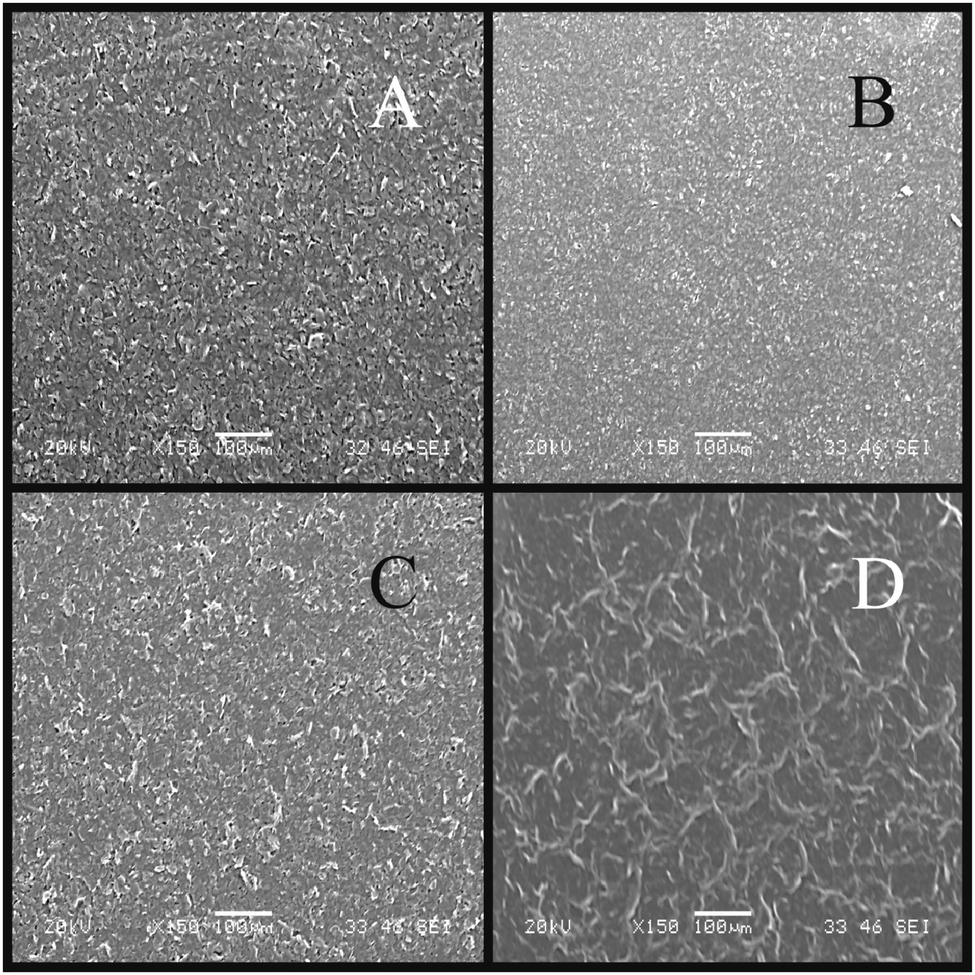 | ||
| Fig. 2 SEM images of the various SPEs: ESPE (A); BSPE (B); GSPE1 (C); and GSPE2 (D). | ||
Raman spectroscopy
Raman analysis was performed to provide further information regarding the graphene/graphitic composition present on the working electrode surfaces of the four SPEs utilised in this work. Fig. 3 depicts the Raman spectra obtained for each electrode. Fig. 3A is typical of the ESPE. The band observed at 1580 cm−1 is typical of graphite,48 and is accompanied by a band at 1355 cm−1 which is characteristic of graphitic defects typically observed in commercially available graphite samples.49 The presence of a small peak at 2700 cm−1 (relative to the peak height of the 1580 cm−1 band) is also representative of graphite. Similarly, for the BSPE these three characteristic bands are observed in Fig. 3B. The graphitic structure is strikingly similar for these two electrodes; it is the difference in polymeric binder percentages between them which gives the electrodes the edge or basal-like rate kinetics.41 Next we turn to characterising our two GSPEs. Through inspection of Fig. 3C, it is clear that there are no apparent differences in the graphitic structure for GSPE1 in comparison to that of the previous two electrodes (viz. ESPE and BSPE). Conversely GSPE2 (Fig. 3D) exhibits a large characteristic graphene band at 2710 cm−1 which has an intensity lower than the characteristic graphite peak at 1580 cm−1 yet does not exhibit the characteristics of that expected for graphite. Literature reports attribute this to few layer graphene, likely in the region of n = 6–8 where n is the number of graphene layers.50,51 This is despite the manufacturer claiming that single-layer graphene is utilised and thus, though this may be the case, it is likely that the graphene platelets flocculate and stack whilst in the ink, forming stacked graphite-like (few-layer graphene) structures as previously reported to be the case when utilising graphene paste electrodes.20 Additionally this is complicated further through the incorporation of the polymeric binder. Hence from the two GSPEs fabricated, one might expect GSPE2 to exhibit more graphene-like electrochemistry. Indeed, the SEM images obtained for the GSPE2 (Fig. 2D) show a surface that is akin to a graphene-like structure and thus the Raman spectrum and SEM combined confirms this observation.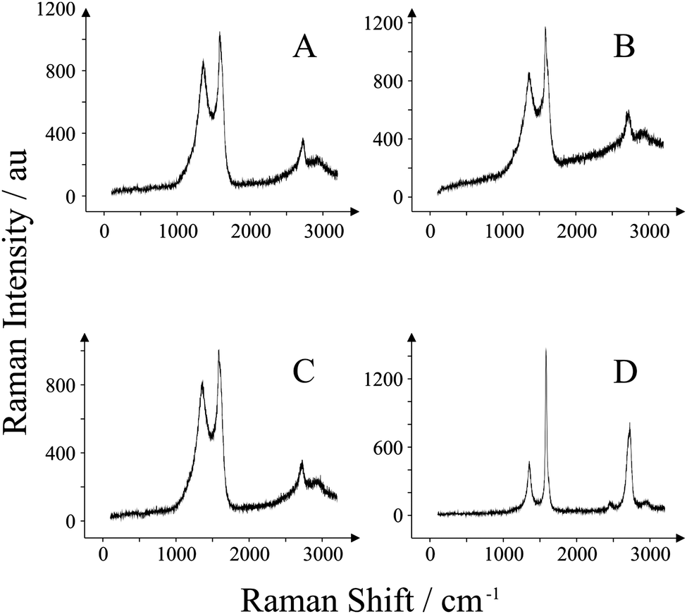 | ||
| Fig. 3 Raman spectra obtained for each of the SPEs utilised: ESPE (A); BSPE (B); GSPE1 (C); and GSPE2 (D). | ||
X-ray photoelectron spectroscopy
XPS was performed with the spectra obtained to de-convolute the different types of graphitic species and surface terminations present upon the surface of the fabricated screen-printed electrodes. The XPS spectra of the major components (C1s and O1s) are shown in Fig. S1 and S2 (ESI†) for GSPE1 and GSPE2, respectively. Table 1 lists the surface compositions of both electrodes in atomic percentage (at%). The GSPE1 (ESI,† Fig. S1) sample surface is dominated by graphitic material and a chlorinated hydrocarbon, likely due to the use of a PVC binder (though the exact origin of this is unknown as ink compositions, especially binders, are proprietary information of the manufacturing company), along with traces of silicon and sulphur (probably as an organic sulphide). The C1s (ESI,† Fig. S1A) spectrum is complex due to the peak shape of the graphitic material which is very asymmetric; this includes a long tail to high binding energy which overlaps with the chlorinated hydrocarbon, where both obscure any oxygenated functionality. The O1s (ESI,† Fig. S1B) peak shows no evidence of structure and is difficult to define precisely but some form of alkoxy (C–O) species is likely.| Element | GSPE1 | Element | GSPE2 |
|---|---|---|---|
| Carbon | 87.70 | Carbon | 86.80 |
| C–H | 3.40 | C–C:C–H | 64.80 |
| C–C | 48.60 | C–O | 8.70 |
| CH2–CHCl | 14.30 | Tail 1 | 7.40 |
| CHCl | 14.30 | Tail 2 | 5.90 |
| Tail 1 | 4.70 | Total | 86.80 |
| Tail 2 | 2.40 | ||
| Total | 87.70 | Oxygen | 11.97 |
O![[double bond, length as m-dash]](https://www.rsc.org/images/entities/char_e001.gif) C C |
0.63 | ||
| Chlorine | 9.22 | O–C–C | 10.34 |
| Oxygen (organic) | 2.94 | O–C–O | 1.00 |
| Silicon | 0.06 | Total | 11.97 |
| Sulphur | 0.08 | ||
| Silicon | 0.16 | ||
| Iron | 0.30 | ||
| Manganese | 0.08 | ||
| Sulphur, S– | 0.21 | ||
| Sulphur, SOx | 0.39 | ||
| Bromine | 0.09 |
The GSPE2 (ESI,† Fig. S2) sample surface is different to GSPE1 in that there is no evidence of a chlorinated hydrocarbon. The indications are that the surface is mostly graphitic in nature with a substantial level of surface oxidation that is difficult to define precisely due to the asymmetric shape and tail of the graphitic C1s peak (ESI,† Fig. S2A). There is, however, good evidence for some form of alkoxy (C–O) species in both the C1s and O1s (ESI,† Fig. S2B) spectra. There are traces of silicon, iron, manganese, sulphur (as sulphide and a sulphate/sulphonate) and bromine.
XPS characterisation of the ESPE and BSPE have been performed and reported previously; a more detailed discussion can be found in original works by Gomis-Berenguer et al.47 In their work, the ESPE was found to comprise of 85.9% surface carbon, displaying graphitic, C–O, and carbonyl groups at 284.5 eV (65.3%), 285.7 eV (10.5%), and 286.6 eV (10.1%), respectively. The BSPE exhibited similar levels of surface carbon (87.5%), however only graphitic and C–O groups were observed at 284.2 eV (80.5%) and 285.6 eV (7.0%), respectively. It is noteworthy too that there is a higher percentage of oxygenated functionalities at the ESPE surfaces, making the electrode more hydrophilic and thus more electrochemically active in aqueous solutions.47
Finally the XPS spectra have been de-convoluted to show a range of O/C ratios: 0.315 (ESPE); 0.087 (BSPE); 0.034 (GSPE1); and 0.138 (GSPE2). Surface oxygen content in some cases has a major effect upon observed electrochemical responses and as such these ratios shall have to be considered in the electrochemical characterisation.
Attenuated total reflectance spectroscopy
Fig. S3 (ESI†) illustrates the average ATR spectra for both graphene inks (analysed as-received and in their ‘wet’ form) being studied within this paper. In GSPE2, there is a broad peak at ∼1049 cm−1, and a similar band is observed for GSPE1 at ∼1132 cm−1. Such bands are typical of C–O bonds appearing in ethers, esters, alcohols or phenol compounds, though XPS conflicts with the report for GSPE1 as the XPS data suggests very little surface oxidation. Hence, the peak at 1132 cm−1 is attributed to the solvent utilised within the ink (diacetone alcohol). Next we see a prominent band in the GSPE1 sample at 1353 cm−1, which is typical of sp3 hybridised bending modes. Interestingly, this type of mode does not exist in the GSPE2 sample. There is a prominent sharp band at 1670 cm−1 in the GSPE1 sample which is typical of CO groups; most probably carboxylic acid groups. The shoulder observed at the CO band on the GSPE1 sample at 1714 cm−1 is indicative of –COOH species according to Chen et al., whereas in the GSPE2 ink the CO band appears at approximately 1659 cm−1 which is more likely to be the deprotonated carboxylate species.52 The carboxylic acid idea is rationalised here by the appearance of the broad wave at 3400 cm−1 which is typical of various types of –OH modes, however it is noted that the sample was introduced to the ATR spectrometer as a paste and hence there is solvent in the sample which will contribute to this. There is another high frequency triplet band noted in both cases at 2971 cm−1. Reports suggest this is a stretching mode of sp3 hybridised C–H groups.53 While this makes little sense in terms of a graphene structure as graphene is sp2 hybridised, it is reasonable to suggest that the ink is comprised of a variety of carbon structures including some sp3 hybridised terminating species (such as carbon black which in dispersed in the GSPE1 ink) and the organic solvents (diacetone alcohol in the case of GSPE1 and hexanol in the case of GSPE2) suspending the carbon structures also exhibit sp3 hybridised bonds and could be responsible for the C–H bonds observed in the ATR spectra.
Summary: physicochemical characterisation
In summary, we can conclude from SEM imaging that the surface morphologies of the ESPE and GSPE1 electrodes are strikingly similar and hence could potentially behave in a similar electrochemical manner, whereas the GSPE2 electrode appears to exhibit more basal(graphene)-like character and will likely exhibit an electrochemical response more akin to that of the basal plane-like BSPE electrode (truly graphene like). Raman analysis of the electrodes confirms that GSPE2 is the most ‘graphene-like’ electrode fabricated, whereas the other SPEs are largely graphitic (graphite-like) in nature. The O/C ratios are 0.315, 0.087, 0.034, and 0.138 for ESPE, BSPE, GSPE1, and GSPE2, respectively. These O/C ratios arise not only from the graphene structures but from other constituents used in the ink fabrication process (solvents, polymeric binders, carbon black). Since the oxygenated groups can affect the voltammetric response, depending on which probe is utilised, it is hard to de-convolute the electrochemical origin of the screen-printed graphene electrode response, i.e. electronic structure (DoS) or O/C composition. Nevertheless, these screen-printed graphene inks are novel; hence we turn to de-convoluting their electrochemical behaviour towards a selection of electrochemical probes.Electrochemical characterisation
This section focuses on the electrochemical characterisation of the GSPEs utilising the widely known and utilised electrochemical redox probes, hexaammine-ruthenium(III) chloride, potassium ferrocyanide(II), and N,N,N′,N′-tetramethyl-p-phenylenediamine (TMPD). We then investigate the electrochemical responses of biologically relevant analytes such as ascorbic acid (AA), β-nicotinamide adenine dinucleotide (NADH), uric acid (UA) and dopamine hydrochloride (DA).We first consider performing appropriate background ‘blank’ scans. Fig. 4 depicts cyclic voltammetric curves for the four electrodes in pH 7.4 PBS (0.1 M) only (no redox probe). It is clear that in the case of ESPE, BSPE, and GSPE1 the electrodes have comparable wide potential windows, ranging from approximately −0.6 to +1.0 V (vs. Ag/AgCl) which are voltammetrically useful. Of interest is the GSPE2 which exhibits unusual voltammetric behaviour. In the positive potential region there is a redox couple, likely originating from the polymeric binder or solvent used in its fabrication, and in the negative region there are also other electrochemical processes taking place; note that the exact origin of these electrochemical responses are unknown since the exact information of the ink composition is proprietary information of the ink manufacturer. As a result of these observations, this electrode must be operated within a small potential window (−0.5 to +0.5 V vs. Ag/AgCl) otherwise these voltammetric profiles observed in the blank will voltammetrically interfere; we continue to investigate the severity of this towards our selected redox probes.
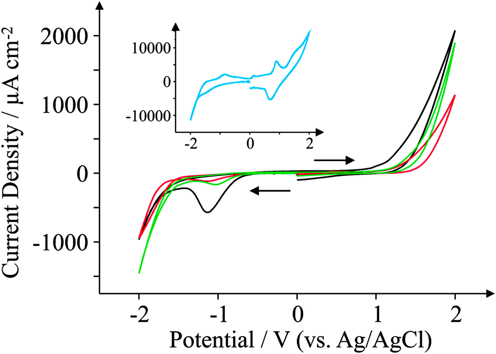 | ||
| Fig. 4 Background ‘blank’ cyclic voltammograms obtained in pH 7.4 PBS (0.1 M) only. All recorded at a scan rate of 100 mV s−1: ESPE (black); BSPE (red); GSPE1 (green); and GSPE2 (blue; inset). | ||
Hexaammine-ruthenium(III) chloride
Attention was next turned to exploring the voltammetric response of the screen-printed electrodes with hexaammine-ruthenium(III) chloride, a commonly used redox probe for the electrochemical characterisation of electrode surfaces;54–56Fig. 5 depicts the observed redox behaviour of the four SPEs. Analysis of the voltammetric profiles is undertaken in terms of the voltammetric peak-to-peak potential (ΔEp) of the oxidation and reduction where a ΔEp of 59 mV (298 K) is the reversible limit; generally the smaller the ΔEp (up to the reversible limit) the more reversible the electrochemical process is.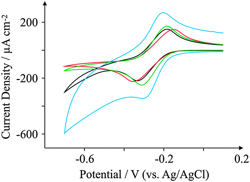 | ||
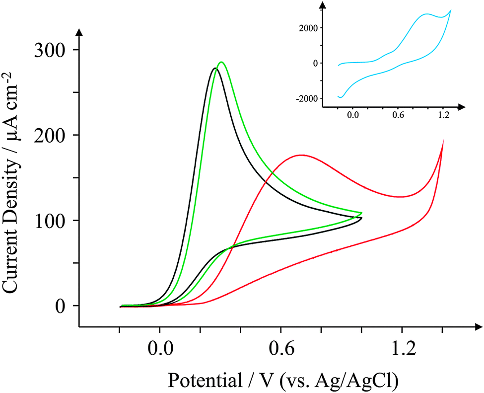
| Fig. 5 Cyclic voltammograms obtained for 1 mM hexaammine-ruthenium chloride in pH 7.4 PBS. All recorded at a scan rate of 100 mV s−1: ESPE (black); BSPE (red); GSPE1 (green); and GSPE2 (blue). | ||
Analysis of the voltammetric profiles (recorded at 100 mV s−1) presented in Fig. 5 reveal that the GSPE2 exhibits a ΔEp of 102 mV whereas GSPE1 exhibits a slightly higher value of 127 mV while the ESPE has a ΔEp of 146 mV and the BSPE a ΔEp of 202 mV. The peak-to-peak separation of the BSPE electrode (ΔEp = 202 mV) is largely expected due to the electrode containing a high binder percentage, which effectively blocks fast electron transport at the carbon structure.41 It is worth noting here that the basal-like voltammetry observed for the BSPE electrodes is not an effect of electronic anisotropy, rather the composition of the ink; hence we prefer to term the electrode “basal plane-like’’ rather than a basal plane SPE. To further characterise the screen-printed electrodes the heterogeneous electron transfer rate constant, k0 was deduced as described by eqn (1) and (2). The electron transfer rate constants of hexaammine-ruthenium(III) chloride for the four electrodes were found to correspond to: 3.36 × 10⁻³, 2.09 × 10⁻³, 3.68 × 10⁻³ and 4.07 × 10⁻³ cm s−1 for the ESPE, BSPE, GSPE1 and GSPE2 respectively. To ensure a diffusional process was indeed proceeding without thin-layer effects, the peak current was monitored as a function of the applied scan rate. Analysis of a plot of log10![[thin space (1/6-em)]](https://www.rsc.org/images/entities/char_2009.gif) Ipversus log10ν revealed a linear gradient of around 0.5 for all the cases (range 0.45–0.51) which is indicative of a diffusional process without thin-layer effects as noted in the case of carbon nanotubes57 and the absence of a porous surface which is in agreement with SEM images presented earlier.
Ipversus log10ν revealed a linear gradient of around 0.5 for all the cases (range 0.45–0.51) which is indicative of a diffusional process without thin-layer effects as noted in the case of carbon nanotubes57 and the absence of a porous surface which is in agreement with SEM images presented earlier.
Previous reports regarding the observed electrochemical responses of this probe with electronically anisotropic carbon materials show electron transfer process to be unhindered with an electrode surface comprising high basal plane density,58 that is, a small proportion of edge plane like-sites/defects are required in order to observe near reversible voltammetric profiles. However, going against this trend, recently Brownson et al. have explored mono-layer graphene, few layered (termed quasi-graphene) graphene and double layer graphene with edge plane and basal plane electrodes fabricated from HOPG and found that the voltammetric response correlates with the proportion of edge plane sites;59 that is, in this limit, the lower global percentage of edge plane sites results in voltammetric profiles with large ΔEp values for a surface with a high basal plane content and low proportion of edge plane sites/defects.59 The surface oxygen content of the respective electrodes has no apparent effect upon the observed voltammetric profiles for hexaammine-ruthenium(III) chloride. If one compares the experimentally observed electrochemical reactivities of the electrodes (ordered fastest to slowest) one can arrange them in the order GSPE2 > GSPE1 > ESPE > BSPE, which bears no correlation to the surface oxygen content of the electrodes which appear in the order ESPE > GSPE2 > BSPE > GSPE1. This is consistent with the literature reporting that the Density of States (DoS) rather than the oxygenated species present at the electrode surface dominant the electrochemical response towards this redox probe.60 The observed electrochemical reactivity indicates that the ESPE and GSPE1 behave similarly which is consistent with the physicochemical characterisation presented above. However, it must be pointed out that the origin of the electrochemical reactivity of the GSPE2 which gives the best response in terms of electron transfer cannot be completely de-convoluted. This is a result of the ink manufacturer withholding proprietary information concerning the ink formation which is necessary to definitively ascribe the background voltammetry. However we can state that there are impurities found via XPS which contribute to the voltammetric responses as well as structural components (graphene) as identified by Raman spectroscopy. The relative contribution of these components to the voltammetry is however impossible to identify at this time.
Potassium ferrocyanide(II)
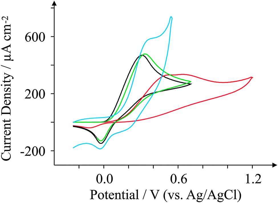
The electrochemical properties of the GSPEs are further explored by observing the redox behaviour of potassium ferrocyanide(II), a frequently used redox probe27,61,62 for characterising electrode surfaces which is a probe known to be surface sensitive, requiring a specific surface interaction for electron transfer to proceed:60,63i.e. C–O groups, their quantity and form. Fig. 6 depicts typical voltammetric profiles observed for the four in-house fabricated SPEs at 100 mV s−1, where we notice very different voltammetric behaviours between the two new graphene SPEs. The edge plane-like ESPE electrode exhibits a ΔEp of 234 mV, while the basal plane-like BSPE electrode exhibits a far larger ΔEp of 510 mV. GSPE1 exhibits characteristic redox behaviour more akin to edge plane-like carbon electrodes with a ΔEp of approximately 276 mV, and GSPE2 exhibits a ΔEp of 671 mV. The response observed at GSPE2 cannot be considered, due to (as mentioned above) its inherent impurities. The reactivity of ESPE > GSPE1 > BSPE can be taken into account in terms of GSPE1 being highly graphitic in nature according to the Raman analysis and thus exhibits more graphite-like electrochemical characteristics than that of basal plane carbonaceous material (BSPE) and where ESPE has a greater oxygen content over that of GSPE1 giving rise to slightly faster electron transfer. Additionally, the BSPEs response is as expected given its low oxygen content and edge plane composition.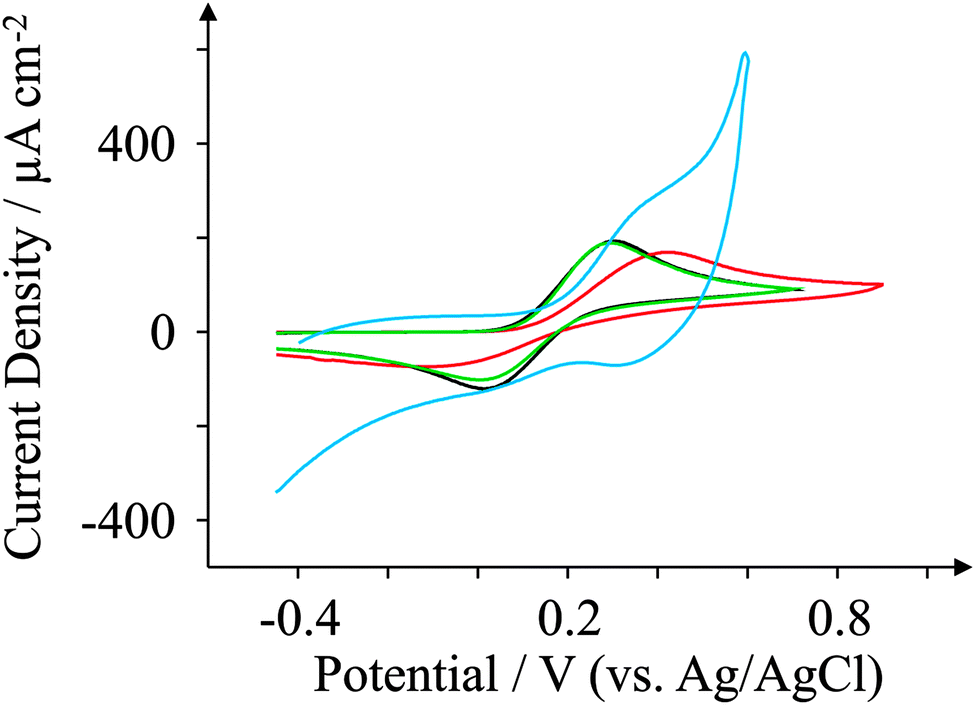 | ||
| Fig. 6 Cyclic voltammograms obtained for 1 mM potassium ferrocyanide in pH 7.4 PBS. All recorded at a scan rate of 100 mV s−1: ESPE (black); BSPE (red); GSPE1 (green); and GSPE2 (blue). | ||
TMPD
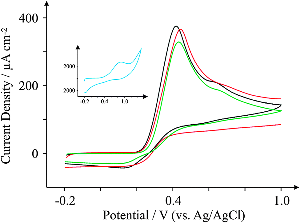
Another commonly used probe in electrochemistry is N,N,N′,N′-tetramethyl-p-phenylenediamine, or TMPD. TMPD is an outer-sphere redox probe utilised by many due to its versatile and unique voltammetric profile which exhibits two near-reversible peaks (over a large potential sweep) in organic and aqueous solvents as well as in ionic liquids.64,65 Here we use the first reversible process only which activates at around 0.0 V (vs. Ag/AgCl). Fig. 7 presents voltammetric curves obtained for the four electrodes utilising 1 mM TMPD at 100 mV s−1. The oxidation process occurs at low potentials for all four electrodes utilised here. For ESPE, the ΔEp corresponds to 256 mV, similar to that observed for BSPE which exhibits a ΔEp of 249 mV. However both graphene-based electrodes are shown to exhibit reduced peak-to-peak separations compared to graphite-based alternatives; GSPE1 exhibits a ΔEp of 149 mV, whilst GSPE2 exhibits a ΔEp of 93 mV. Since TMPD is known to be dependent on the content of edge plane sites, the response of the GSPE1 is not expected or predicted from prior work on graphitic electrodes. The response at the GSPE2 likely is a result of impurities in the ink while the response of the GSPE1 is unknown; due to the composition of the ink being completely unknown, such control experiments to determine the origin of this cannot be conducted.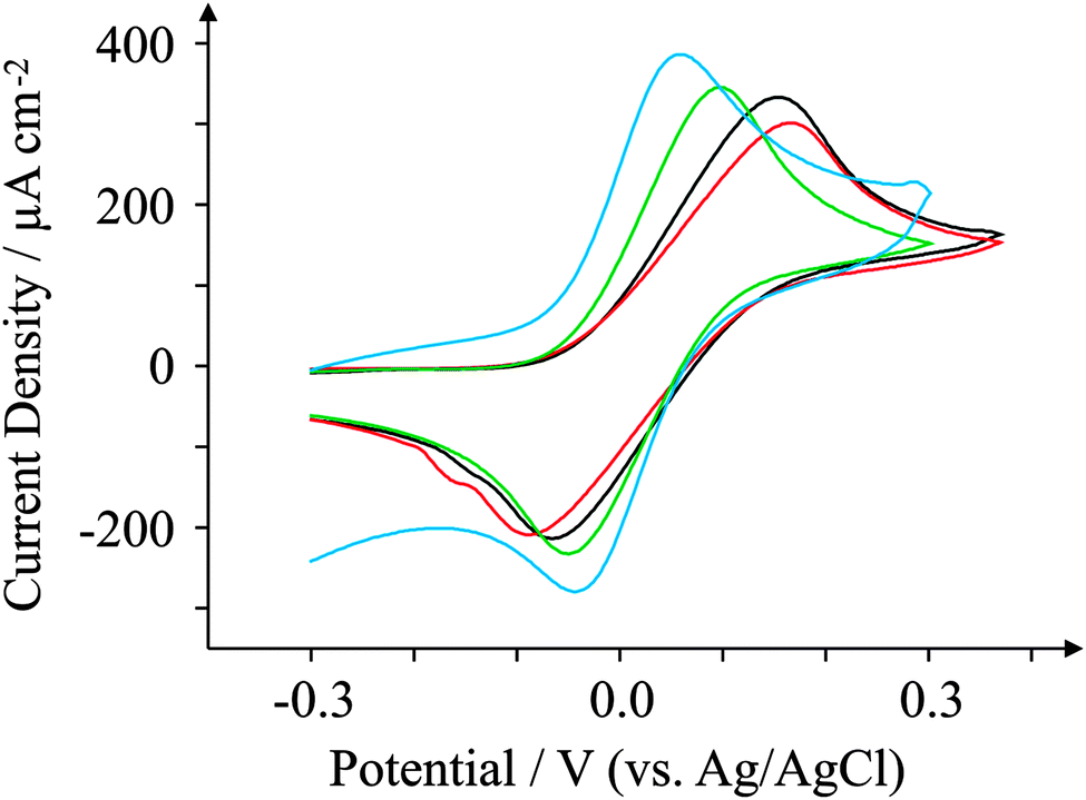 | ||
| Fig. 7 Cyclic voltammograms obtained for 1 mM TMPD in pH 7.4 PBS. All recorded at a scan rate of 100 mV s−1: ESPE (black); BSPE (red); GSPE1 (green); and GSPE2 (blue). | ||
NADH
We turn our attention now to NADH, a commonly used electroactive analyte used due to its involvement as a cofactor in enzymatic reactions.66 The electrochemical performance of NADH is reported in the literature to be dependent on the density of edge plane-like sites residing on the electrode surface.21Fig. 8 reveals the oxidation of NADH (all recorded at 100 mV s−1) to occur at +0.61 V for the case of the GSPE1 which is similar to the response observed for the ESPE exhibiting a peak potential of +0.57 V. The peak heights for GSPE1 and ESPE (at 100 mV s−1) were found to correspond to 261 and 283 μA cm−2, respectively; the electroanalytical utility of these electrodes is explored later. Referring to the similar surface morphologies (SEM etc.) which are strikingly similar, it comes as no surprise that these electrodes behave similarly towards NADH. Conversely the peak potentials for the BSPE and GSPE2, which correspond to +0.94 V and +0.99 V respectively, are much higher than observed for the case of ESPE and GSPE1. The peak heights for BSPE and GSPE2 correspond to 173 and 2394 μA cm−2, respectively. The peak heights in all four cases will be investigated electroanalytically later in this investigation. Similar to previous literature, the voltammetric response observed for NADH in this case appears to be dependent upon the density of edge plane-like sites available.21 A ten-fold increase in current density is observed for the GSPE2; this is rationalised if one observes the blank scans as depicted in Fig. 4. The oxidation potentials for NADH at a GSPE2 electrode are higher than +0.6 V (vs. Ag/AgCl) which results in the voltammetric response for NADH combining with the background response observed in Fig. 4.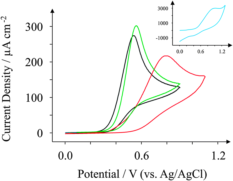 | ||
| Fig. 8 Cyclic voltammograms obtained for 1 mM NADH in pH 7.4 PBS. All recorded at a scan rate of 100 mV s−1: ESPE (black); BSPE (red); GSPE1 (green); and GSPE2 (inset; blue). | ||
Ascorbic acid, uric acid and dopamine
Ascorbic Acid (AA) is another commonly used electroactive analyte which is important not only as it is an antioxidant,67 but also because urinary concentrations can be high and can interfere with desired urinary target analytes such as the neurotransmitter68 dopamine (DA) or uric acid (UA, a molecule associated with gout).69 Consequently, a cornucopia of studies focus their attention on ‘separating out’ the signals observed for the aforementioned analytes.70–74 We have taken the opportunity within this section to observe the electrochemical behaviour of our graphene SPEs towards those erstwhile target analytes.Fig. 9–11 depict cyclic voltammograms obtained at 100 mV s−1 for 1 mM AA, DA, and UA respectively (each separately presented in solution) at the four electrodes used within this work, where some interesting developments are observed in terms of peak potentials. In the case of AA, the expected peak potential of +0.27 V is observed for the ESPE electrode as has been observed previously for edge plane electrodes.19 We also see that the basal plane-like BSPE electrode exhibits a peak potential of +0.71 V as one may expect due to the slower electron transfer rate kinetics generally exhibited by such an electrode. In the case of the graphene electrodes, GSPE1 exhibits similar voltammetry to the ESPE electrode (Ep = +0.31 V) as has been the case on numerous instances throughout this paper, yet GSPE2 exhibits a further increase in peak potential corresponding to +0.98 V, clearly originating from its graphene-like nature/composition (low edge plane content). In the case of DA, a different response is observed. The ESPE and BSPE electrodes exhibit peak potentials of +0.31 and +0.63 V respectively, whilst GSPE1 exhibits a peak potential of +0.34 V and GSPE2 exhibits a peak potential of +0.40 V. The observation at the GSPE2 is interesting as it does not fall within the same potential range as the peak potential observed for AA; therefore said electrode could have a potential use for the simultaneous detection of AA and DA. However, the peak potential of UA utilising GSPE2 is +0.82 V, which is similar to that observed towards AA and hence one envisages issues for simultaneous detection of these two target analytes at this electrode. It is also noted that the current densities for GSPE2, as seen in the case of NADH, AA, and UA, are far larger than the other SPEs utilised in this work. This is due to the activation potentials of NADH, AA, and UA being over +0.6 V for the case of GSPE2, and thus there is background interference from the constituents of the electrode contributing to the overall voltammetric response (as shown in the blank scans in Fig. 4).
 | ||
| Fig. 9 Cyclic voltammograms obtained for 1 mM AA in pH 7.4 PBS. All recorded at a scan rate of 100 mV s−1: ESPE (black); BSPE (red); GSPE1 (green); and GSPE2 (inset; blue). | ||
 | ||
| Fig. 10 Cyclic voltammograms obtained for 1 mM DA in pH 7.4 PBS. All recorded at a scan rate of 100 mV s−1: ESPE (black); BSPE (red); GSPE1 (green); and GSPE2 (blue). | ||
 | ||
| Fig. 11 Cyclic voltammograms obtained for 1 mM UA in pH 7.4 PBS. All recorded at a scan rate of 100 mV s−1: ESPE (black); BSPE (red); GSPE1 (green); and GSPE2 (inset; blue). | ||
Summary: electrochemical characterisation
Generally, it has been observed that the electrochemical reactivities of the ESPE and GSPE1 electrodes are similar and therefore it can be concluded that the DoS for the ESPE and GSPE1 are similar, that is, the ratio of edge and basal plane sites is similar. This is particularly apparent in the case of electrochemical redox probes studied and the biologically relevant analytes (NADH, AA, UA, DA) where it is observed that the DoS drastically affects the observed voltammetric profiles. Comparing to the physical characterisations presented above, where high amounts of edge plane-like sites/defects are observed for ESPE and GSPE1, such observations are in agreement with the relative surface structures. It is likely that the graphene utilised in the ink for GSPE1 undergoes coalescence in the ink medium which results in multilayer graphene structures within the ink (a phenomenon observed previously for graphene paste electrodes).75 On the other hand, the GSPE2 electrodes exhibit dramatically different voltammetric behaviour which is likely due to the impurities within the ink. While the voltammetric responses are illuminating, fundamental insights from these electrodes cannot be revealed since the exact composition on the ink is proprietary information.The advantage of this range of carbon substrates of course lies within the tailoring of the heterogeneous electron transfer rate constant. For instance if one requires a slower electron transfer rate (such as in energy applications), GSPE2 or BSPE may be a wise choice given their slow electron transfer kinetics. Given that there are larger differences in electron transfer rates between the two electrodes, both inks could potentially be used depending upon the specific needs of the system. Furthermore the percentage of polymeric binders can easily be modified in the electrode ink to change the required electron transfer rate constant. Conversely, in the cases where fast heterogeneous electron transfer is required (such as in electroanalytical applications), the ESPE or GSPE1 electrodes are favourable.
Capacitance and resistivity investigation
The capacitative properties of our newly printed electrodes are investigated. In order to do this via cyclic voltammetry, the electrodes are scanned between a potential range of 0.0 to +0.8 V in 1 M Na2SO4. Fig. S4 (ESI†) depicts cyclic voltammograms in 1 M Na2SO4 for each electrode investigated within this work, where it is noted that there is little capacitative behaviour attributed to all four electrodes. We believe this to be a result of the planar surfaces exhibited by the printed electrodes, as confirmed by the SEMs for each. The lack of capacitative effects associated with the electrodes is beneficial in terms of electroanalysis as the currents observed by the electrodes will not be “masked” by capacitative behaviour and hence limits of detection for such electrodes will effectively be lower.The resistivity of all of our electrodes utilised was explored using a DVM. Table 2 lists the average resistance obtained for each electrode (N = 5) and the corresponding % RSD. From the resultant resistance tests, we note that the ESPE exhibits an average resistivity of 56.3 Ω cm, while the BSPE exhibits an average resistivity of 89.1 Ω cm. GSPE1 exhibits a relatively low resistivity of 41.8 Ω cm, whereas GSPE2 exhibits an extremely low average resistivity of 8.9 Ω cm. This is unsurprising as one would expect a true graphene structure to exhibit a very low resistivity.
| Electrode | Resistivity/Ω cm | % RSD |
|---|---|---|
| ESPE | 56.3 | 8.9 |
| BSPE | 89.1 | 4.8 |
| GSPE1 | 41.8 | 14.4 |
| GSPE2 | 8.9 | 1.6 |
Electroanalytical properties
We now explore whether our electrodes are suitable to detect typical electroactive molecules in an analytical context. Fig. 12 depicts a calibration graph typical of the peak current density observed as a function of concentration of AA in pH 7.4 PBS. Such a high analytical range (approximately 1–10 mM) is in contrast to the case of DA sensing, as the concentrations of AA observed within urine are generally higher than other molecules such as DA.76 All of the electrodes studied exhibit a linear correlation in current density with respect to the concentration of AA. Paying particular attention to GSPE2, we note a linear range (current density (j) = 130.40 μA cm−2 mM−1–52.30 μA cm−2; N = 11; R2 = 0.98) with a Limit of Detection (LoD) (3σ) of 0.68 mM. Such a linear regression over this range is satisfactory for the electroanalytical detection of AA, though it would be preferable to improve the error of the electrodes, and thus the regression coefficient, to facilitate a more accurate AA sensor. This lack of sensitivity is exemplified by studying the reproducibility of the GSPE2 electrode. The GSPE2 electrode exhibited %RSD values as high as 26% over ten additions during electroanalysis. Comparably, the ESPE exhibited a maximum %RSD of 4% and the GSPE1 4%.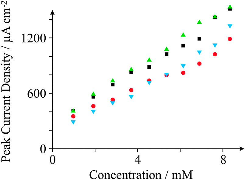 | ||
| Fig. 12 Calibration plots depicting ‘peak height versus concentration’ towards the detection of AA in pH 7.4 PBS at 100 mV s−1 (vs. Ag/AgCl) utilising the various SPEs: ESPE (black squares); BSPE (red circles); GSPE1 (green triangles); and GSPE2 (blue inverted triangles). | ||
Similarly, DA was tested electroanalytically utilising concentrations typically found in bodily fluid at normal (approximately 65–400 μg per day, equating to approximately 1–10 μM)77 and abnormal levels as typically observed in substance abusers, thrill seekers and insomniacs. The results for all four electrodes towards the detection of AA and DA are depicted in Table 3. Upon comparison of the relative sensitivities of each electrode towards both analytes, a different pattern is observed for both target analytes. In the case of AA, the relative sensitivities are (listing the highest current density per mM first): GSPE1 > ESPE > BSPE > GSPE2. Conversely for DA, the relative sensitivities (highest sensitivity per μM) are ESPE > GSPE2 > GSPE1 > BSPE. These trends can be explained in terms of the surface sensitivities of the relevant target analytes. DA is known to be highly sensitive to oxygenated species and as such will nucleate and at oxygenated moieties upon an electrode surface;78 hence, it would be expected that ESPE and GSPE2 exhibit a more profound reaction with DA as they are the two electrodes which exhibit the highest amount of oxygenated species according to our XPS results. Thus, such an interaction with oxygenated species will facilitate electron transfer and consequently an increased response observed with respect to increasing concentrations of DA. AA on the other hand is not sensitive to oxygenated species and hence it is the DoS which affects the electro-oxidation of AA. Therefore we would typically expect to see either GSPE1 or ESPE being the most sensitive to AA due to a high density of edge plane sites and GSPE2 being the least sensitive given its surface configuration being predominantly a graphene basal plane according to our Raman data.
| Analyte | Electrode | LoD/AA: mM; DA: μM | Sensitivity/(AA: μA cm−2 mM−1; DA: μA cm−2 μM−1) |
|---|---|---|---|
| Ascorbic acid (AA) | ESPE | 0.53 ± 0.01 | 10.46 |
| BSPE | 0.51 ± 0.03 | 7.16 | |
| GSPE1 | 0.35 ± 0.01 | 11.07 | |
| GSPE2 | 0.68 ± 0.08 | 1.02 | |
| Dopamine hydrochloride (DA) | ESPE | 3.35 ± 0.04 | 0.66 |
| BSPE | 4.41 ± 0.12 | 0.34 | |
| GSPE1 | 1.60 ± 0.03 | 0.57 | |
| GSPE2 | 8.08 ± 0.29 | 0.60 | |
It is an exciting prospect that a mass producible graphene-based electrode exhibits such excellent electroanalytical properties for model target analytes; coupled with the fact that the electrochemical activation potentials are spread across a wider concentration range. The GSPE2 electrode has a potential application for urinary analysis of AA and DA. One major limitation however that needs addressing with the GSPE2 is that the analytical reproducibility is currently very poor, with some % RSD measurements as high as 26%. Conversely the ESPE, BSPE, and GSPE1 exhibit % RSD values corresponding to no more than 5%; this is what many would describe as analytically acceptable. It is clear that the graphene-based SPEs can be utilised electroanalytically if the reproducibility drawback is overcome, and further they could potentially be used for simultaneous detection of urinary analytes such as DA and AA as these reported analytical ranges are suitable for the detection of these analytes in urine samples, see for example;76,77 this will be the focus of our future work. While such printed electrodes show no benefit over the likes of conventional electrode substrates such as EPPG, they do offer the benefit of tailoring the heterogeneous electrochemical response through the use of polymeric binders, and are easy to use, disposable, and more critically, reproducible. Furthermore, in terms of producing graphene electrodes on a mass scale, screen-printed technologies are the front runner, ahead of paste electrodes as screen-printed electrodes are more reproducible, and ahead of conventional electrodes as they are far cheaper and quicker to fabricate.
Conclusions
This work has demonstrated, for the first time, the fabrication of a true screen-printable graphene ink. The inks utilised in this work exhibit dramatically different electrochemical properties towards a range of analytes, with the responses shown to exhibit noticeable changes depending on the DoS and binder content and also (although to a lesser extent) exhibit distinct electrochemical responses with respect to the presence of surface oxygenated species. The experiments presented within this paper offer a proof-of-concept approach for screen-printed graphene electrode designs. One of the fabricated graphene electrodes exhibited slow electron transfer properties (potentially beneficial for energy applications) and the other electrode was found to exhibit fast electron transfer kinetics (which can be beneficially employed where fast electron transfer is required, i.e. in electroanalysis) demonstrating that graphite control experiments are critical when investigating any type of graphene electrode. Unfortunately, until ink manufacturers declare the exact composition of their graphene (and graphitic) inks, fundamental graphene electrochemistry is precluded. A thorough understanding of the ink compositions could potentially lead to a mass-producible disposable screen-printed graphene electrode which would be extremely useful for fundamental graphene electrochemistry as it would remove the need for laborious graphene production strategies (scotch tape method, Hummers, CVD etc.) and effectively speed up the research in this area. To achieve this, the graphene inks need be modified accordingly by changing the type of graphene and removing electroactive background components. We shall be working with the company to source the origin of this background voltammetry, however, the majority of our electrochemical tests in this work indeed point to a quasi-graphene-like screen printed electrode. Nevertheless, we have demonstrated that useful electrochemical responses can be obtained from such electrodes, but caution has to be paid to the excitation potential of the target analyte of interest.The differing electrode characteristics were achieved due to the inks offering a range of electron transfer rates with one effectively able to tailor the electrode material to suit the application required; these may be implemented for specific purposes depending upon the desired electron transfer rate for a given system, whilst at the same time being mass producible and thus easily accessible for a relatively small cost. Furthermore, these inks can be printed into various shapes, diameters, bands, and arrays with little effort required to modify the electrode design.79–81 Consequently, in this paper we have presented the fabrication and characterisation of what we believe to be the first real GSPEs which can be printed via screen-printing technology over numerous printing cycles and have an ink screen life of more than three hours. This approach utilises newly commercially available printable graphene inks from reputable screen-printing companies instead of lab-synthesized graphene.
References
- Y. Zhu, S. Murali, W. Cai, X. Li, J. W. Suk, J. R. Potts and R. S. Ruoff, Adv. Mater., 2010, 22, 3906–3924 CrossRef CAS PubMed.
- C. Lee, X. Wei, J. W. Kysar and J. Hone, Science, 2008, 321, 385–388 CrossRef CAS PubMed.
- K. S. Novoselov, D. Jiang, F. Schedin, T. J. Booth, V. V. Khotkevich, S. V. Morozov and A. K. Geim, Proc. Natl. Acad. Sci. U. S. A., 2005, 102, 10451–10453 CrossRef CAS PubMed.
- M. S. Lundstrom, Nat. Mater., 2011, 10, 566–567 CrossRef CAS PubMed.
- F. Xia, V. Perebeinos, Y.-M. Lin and P. Avouris, Nat. Nanotechnol., 2011, 6, 179–184 CrossRef CAS PubMed.
- P. V. Kamat, J. Phys. Chem. Lett., 2011, 2011, 242–251 CrossRef.
- H. Chang, L. Tang, Y. Wang, J. Jiang and J. Li, Anal. Chem., 2010, 82, 2341–2346 CrossRef CAS PubMed.
- S. K. Min, W. Y. Kim, Y. Cho and K. S. Kim, Nat. Nanotechnol., 2011, 6, 162–165 CrossRef CAS PubMed.
- X. Wang, L. Zhi and K. Müller, Nano Lett., 2008, 8, 323–327 CrossRef CAS PubMed.
- E. Yoo, J. Kim, E. Hosono, H.-S. Zhou, T. Kudo and I. Honma, Nano Lett., 2008, 8, 2277–2282 CrossRef CAS PubMed.
- X. Yang, J. Zhu, L. Qiu and D. Li, Adv. Mater., 2011, 23, 2833–2838 CrossRef CAS PubMed.
- D. Prasai, J. C. Tuberquia, R. R. Harl, G. K. Jennings and K. I. Bolotin, ACS Nano, 2012, 6, 1102–1108 CrossRef CAS PubMed.
- K. S. Novoselov, V. I. Fal'ko, L. Colombo, P. R. Gellert, M. G. Schwab and K. Kim, Nature, 2012, 490, 192–200 CrossRef CAS PubMed.
- D. A. C. Brownson, D. K. Kampouris and C. E. Banks, Chem. Soc. Rev., 2012, 41, 6944–6976 RSC.
- D. A. C. Brownson and C. E. Banks, Analyst, 2010, 135, 2768–2778 RSC.
- T. Gan and S. Hu, Microchim. Acta, 2011, 175, 1–19 CrossRef CAS.
- D. A. C. Brownson, D. K. Kampouris and C. E. Banks, J. Power Sources, 2011, 196, 4837–4885 CrossRef PubMed.
- L. Dai, D. W. Chang, J. B. Baek and W. Lu, Small, 2012, 8, 1130–1166 CrossRef CAS PubMed.
- D. A. C. Brownson, L. J. Munro, D. K. Kampouris and C. E. Banks, RSC Adv., 2011, 1, 978–988 RSC.
- L. C. S. Figueiredo-Filho, D. A. C. Brownson, O. Fatibello-Filho and C. E. Banks, Analyst, 2013, 138, 4436–4442 RSC.
- E. P. Randviir, D. A. C. Brownson, M. Gómez-Mingot, D. K. Kampouris, J. Iniesta and C. E. Banks, Nanoscale, 2012, 4, 6470–6480 RSC.
- D. A. C. Brownson and C. E. Banks, Phys. Chem. Chem. Phys., 2012, 14, 8264–8281 RSC.
- Y. Wang, Y. Zheng, X. Xu, E. Dubuisson, Q. Bao, J. Lu and K. P. Loh, ACS Nano, 2011, 5, 9927–9933 CrossRef CAS PubMed.
- A. Ambrosi, A. Bonanni, Z. Sofer and M. Pumera, Nanoscale, 2013, 5, 2379–2387 RSC.
- D. A. C. Brownson and C. E. Banks, Phys. Chem. Chem. Phys., 2011, 13, 15825–15828 RSC.
- D. A. C. Brownson, R. V. Gorbachev, S. J. Haigh and C. E. Banks, Analyst, 2012, 137, 833–839 RSC.
- A. T. Valota, I. A. Kinloch, K. S. Novoselov, C. Casiraghi, A. Eckmann, E. W. Hill and R. A. W. Dryfe, ACS Nano, 2011, 5, 8809–8815 CrossRef CAS PubMed.
- J. P. Metters, R. O. Kadara and C. E. Banks, Analyst, 2011, 136, 1067–1076 RSC.
- J. P. Smith, J. P. Metters, D. K. Kampouris, C. Lledo-Fernandez, O. B. Sutcliffe and C. E. Banks, Analyst, 2013, 138, 6185–6191 RSC.
- J. P. Smith, J. P. Metters, C. Irving, O. B. Sutcliffe and C. E. Banks, Analyst, 2013, 138, 389–400 RSC.
- L. Zhang, L. Yang, L. Zhang, D.-W. Li, D. Karpuzov and Y.-T. Long, Int. J. Electrochem. Sci., 2011, 6, 819–829 CAS.
- D. A. C. Brownson, J. P. Metters, D. K. Kampouris and C. E. Banks, Electroanalysis, 2011, 23, 894–899 CrossRef CAS.
- D. A. C. Brownson and C. E. Banks, Electrochem. Commun., 2011, 13, 111–113 CrossRef CAS PubMed.
- S. Eissa, C. Tlili, L. L'Hocine and M. Zourob, Biosens. Bioelectron., 2012, 38, 308–313 CrossRef CAS PubMed.
- F. Valentini, D. Romanazzo, M. Carbone and G. Palleschi, Electroanalysis, 2012, 24, 872–881 CrossRef CAS.
- D. A. C. Brownson and C. E. Banks, Analyst, 2011, 136, 2084–2089 RSC.
- W. Song, D.-W. Li, Y.-T. Li, Y. Li and Y.-T. Long, Biosens. Bioelectron., 2011, 26, 3181–3186 CrossRef CAS PubMed.
- J. Ping, J. Wu, Y. Wang and Y. Ying, Biosens. Bioelectron., 2012, 34, 70–76 CrossRef CAS PubMed.
- P. M. Hallam and C. E. Banks, Electrochem. Commun., 2011, 13, 8–11 CrossRef CAS PubMed.
- Ceram, http://www.ceram.com, accessed November 2013.
- N. A. Choudry, D. K. Kampouris, R. O. Kadara and C. E. Banks, Electrochem. Commun., 2010, 12, 6–9 CrossRef CAS PubMed.
- M. Khairy, D. K. Kampouris, R. O. Kadara and C. E. Banks, Electroanalysis, 2010, 22, 2496–2501 CrossRef CAS.
- P. M. Hallam, D. K. Kampouris, R. O. Kadara and C. E. Banks, Analyst, 2010, 135, 1947–1952 RSC.
- Haydale, http://www.haydale.com, accessed November 2013.
- Vorbeck, http://vorbeck.com, accessed November 2013.
- I. Lavagnini, R. Antiochia and F. Magno, Electroanalysis, 2004, 16, 505–506 CrossRef CAS.
- A. Gomis-Berenguer, M. Gómez-Mingot, V. Montiel, A. Canals, T. Thiemann, R. O. Kadara, C. E. Banks and J. Iniesta, RSC Adv., 2012, 2, 7735–7742 RSC.
- A. C. Ferrari, J. C. Meyer, V. Scardaci, C. Casiraghi, M. Lazzeri, F. Mauri, S. Piscanec, D. Jiang, K. S. Novoseloc, S. Roth and A. K. Geim, Appl. Phys. Lett., 2006, 97, 187401 CrossRef CAS.
- F. Tuinstra and J. L. Koenig, J. Chem. Phys., 1970, 53, 1126–1130 CrossRef CAS PubMed.
- A. Gupta, G. Chen, P. Joshi, S. Tadigadapa and P. C. Eklund, Nano Lett., 2006, 6, 2667–2673 CrossRef CAS PubMed.
- Y. Y. Wang, Z. H. Ni, Y. Yu, Z. X. Shen, H. M. Wang, Y. H. Wu, W. Chen and A. T. S. Wee, J. Phys. Chem. C, 2008, 112, 10637–10640 CAS.
- J. Chen, M. A. Hamon, H. Hu, Y. P. Chen, A. M. Rao, P. C. Eklund and R. C. Haddon, Science, 1998, 282, 95–98 CrossRef CAS.
- U. J. Kim, C. A. Furtado, X. Liu, G. Chen and P. C. Eklund, J. Am. Chem. Soc., 2005, 127, 15437–15445 CrossRef CAS PubMed.
- S. Alwarappan, A. Erdem, C. Liu and C.-Z. Li, J. Phys. Chem. C, 2009, 113, 8853–8857 CAS.
- A. Andreu, J. W. Merkert, L. A. Lecaros, B. L. Broglin, J. T. Brazell and M. El-Kouedi, Sens. Actuators, B, 2006, 114, 1116–1120 CrossRef CAS PubMed.
- M. Manesse, R. Sanjines, V. Stambouli, R. Boukherroub and S. Szunerits, Electrochem. Commun., 2008, 10, 1041–1043 CrossRef CAS PubMed.
- I. Streeter, G. G. Wildgoose, L. Shao and R. G. Compton, Sens. Actuators, B, 2008, 133, 462–466 CrossRef CAS PubMed.
- M. C. Henstridge, L. Shao, G. G. Wildgoose, R. G. Compton, G. Tobias and M. L. H. Green, Electroanalysis, 2008, 20, 498–506 CrossRef CAS.
- D. A. C. Brownson, S. A. Varey, F. Hussain, S. J. Haigh and C. E. Banks, Nanoscale, 2014, 6, 1607–1621 RSC.
- P. Chen and R. L. McCreery, Anal. Chem., 1996, 68, 3958–3965 CrossRef CAS.
- K. C. Honeychurch and J. P. Hart, Adv. Anal. Chem., 2012, 2, 46–52 CAS.
- M. Pumera, Nanoscale Res. Lett., 2007, 2, 87–93 CrossRef CAS.
- M. C. Granger and G. M. Swain, J. Electrochem. Soc., 1999, 146, 4551–4558 CrossRef CAS PubMed.
- R. G. Evans, O. V. Klymenko, P. D. Price, S. G. Davies, C. Hardacre and R. G. Compton, ChemPhysChem, 2005, 6, 526–533 CrossRef CAS PubMed.
- F. Marken, R. G. Compton, C. H. Goeting, J. S. Foord, S. D. Bull and S. G. Davies, J. Solid State Electrochem., 2001, 5, 88–93 CrossRef CAS.
- N. S. Lawrence and J. Wang, Electrochem. Commun., 2006, 8, 71–76 CrossRef CAS PubMed.
- N. Smirnoff, Curr. Opin. Plant Biol., 2000, 3, 229–235 CAS.
- N. Ben-Jonathan, Endocr. Rev., 1985, 6, 564–589 CrossRef CAS PubMed.
- V. Vitart, I. Rudan, C. Hayward, N. K. Gray, J. Floyd, C. N. A. Palmer, S. A. Knott, I. Kolcic, O. Polasek, J. Graessler, J. F. Wilson, A. Marinaki, P. L. Riches, X. Shu, B. Janicijevic, N. Smolej-Narancic, B. Gorgoni, J. Morgan, S. Campbell, Z. Biloglav, L. Barac-Lauc, M. Pericic, I. M. Klaric, L. Zgaga, T. Skaric-Juric, S. H. Wild, W. A. Richardson, P. Hohenstein, C. H. Kimber, A. Tenesa, L. A. Donnelly, L. D. Fairbanks, M. Aringer, P. M. McKeigue, S. H. Ralston, A. D. Morris, P. Rudan, N. D. Hastie, H. Campbell and A. F. Wright, Nat. Genet., 2008, 40, 437–442 CrossRef CAS PubMed.
- J. Huang, Y. Liu, H. Hou and T. You, Biosens. Bioelectron., 2008, 24, 632–637 CrossRef CAS PubMed.
- K. Iriyama, M. Yoshiura, T. Iwamoto and Y. Ozaki, Anal. Biochem., 1984, 141, 238–243 CrossRef CAS.
- C.-L. Sun, H.-H. Lee, J.-M. Yang and C.-C. Wu, Biosens. Bioelectron., 2011, 26, 3450–3455 CrossRef CAS PubMed.
- A. Safavi, N. Maleki, O. Moradlou and F. Tajabadi, Anal. Biochem., 2006, 359, 224–229 CrossRef CAS PubMed.
- H. R. Zare, N. Nasirizadeh and M. M. Ardakani, J. Electroanal. Chem., 2005, 577, 25–33 CrossRef CAS PubMed.
- L. C. S. Figueiredo-Filho, D. A. C. Brownson, M. Gómez-Mingot, J. Iniesta, O. Fatibello-Filho and C. E. Banks, Analyst, 2013, 138, 6354–6364 RSC.
- M. L. Brigden, D. Edgell, M. McPherson, A. Leadbeater and G. Hoag, Clin. Chem., 1992, 38, 426–431 CAS.
- Medline Plus, http://www.nlm.nih.gov/medlineplus/ency/article/003613.htm, accessed October 2013.
- D. A. C. Brownson, C. W. Foster and C. E. Banks, Analyst, 2012, 137, 1815 RSC.
- F. Tan, J. P. Metters and C. E. Banks, Sens. Actuators, B, 2013, 181, 454–462 CrossRef CAS PubMed.
- J. P. Metters, R. O. Kadara and C. E. Banks, Sens. Actuators, B, 2012, 169, 136–143 CrossRef CAS PubMed.
- J. P. Metters, R. O. Kadara and C. E. Banks, Analyst, 2013, 138, 2516–2521 RSC.
Footnote |
| † Electronic supplementary information (ESI) available. See DOI: 10.1039/c3cp55435j |
| This journal is © the Owner Societies 2014 |