 Open Access Article
Creative Commons Attribution 3.0 Unported Licence
Amine-terminated nanoparticle films: pattern deposition by a simple nanostencilling technique and stability studies under X-ray irradiation
P. R.
Coxon
ab,
J. H.
Ahire
a,
S. P.
Ashby
a,
M. D.
Frogley
c and
Y.
Chao
*a
aEnergy Materials Laboratory, School of Chemistry, University of East Anglia, Norwich, NR4 7TJ, UK. E-mail: y.chao@uea.ac.uk
bDepartment of Materials Science & Metallurgy, University of Cambridge, 27 Charles Babbage Road, Cambridge, CB3 0FS, UK
cDiamond Light Source Ltd, Diamond House, Harwell Science & Innovation Campus, Didcot, UK
First published on 18th February 2014
Abstract
Thin films made up of arrays of amine-terminated silicon nanoparticles (NH2-SiNPs) synthesized by a new evaporation technique have been formed by employing TEM grids as nanostencils. FTIR imaging illustrates the feasibility of the method in nanoscale device fabrication applications. Micro-mapping over areas of the nanoparticle material allows the surface chemistry to be examined. FTIR imaging shows trace amounts of oxide confined to the NP surfaces. Thicker films formed by dropcasting allowed the nanoparticle behaviour to be studied under conditions of extended exposure to 150 eV photons radiation by X-ray photoelectron spectroscopy (XPS). The XPS spectrum was monitored over the Si2p region and the initial peak at 100.53 eV was observed to shift to higher binding energies as irradiation progressed which is indicative of charge trapping within the film. This result has potential consequences for applications where NH2-SiNPs are used in X-ray environments such as in bioimaging where the increasing charge buildup is related to enhanced cytotoxicity.
1. Introduction
Semiconductor nanoparticles (NPs) have attracted wide attention from the scientific research community owing to their unique and highly desirable characteristics that only manifest themselves as bulk materials are reduced to nanometer scales. Following the discovery of the quantum confinement effect upon the density of states in semiconductor NPs the number of applications of NPs or ‘quantum dots’ has risen considerably.1,2 Quantum confinement results in size-dependent bandgaps with highly efficient photoluminescent quantum yields across the visible region with the ability to select the emission wavelength by selective control of the NP size.1 In addition NPs display broad emission and narrow excitation spectra and high photostability.3 The emission mechanisms of semiconductor NPs have been reviewed extensively elsewhere4,5 although for silicon NPs there still remains some debate6 with oxidation and size effects playing a role.7,8 These properties have made NPs highly useful in a wide and ever-expanding range of settings, including optoelectronics,9 solar cells,10 computing,11 lasers12 and clinical imaging.13 The impact of NPs on medicine has been particularly strong and many potential biomedical applications have been reviewed by several authors in recent years.14–17 Since the early 2000s many types of nanoparticles have been routinely employed to help gain a greater understanding of diseases and in the development of more effective detection and treatment methods. An important body of research has focused upon the use of NPs as fluorescent biological markers by exploiting the advantages NPs possess over conventional luminescent dyes within in vitro and in vivo systems,18–20 and as carrier bodies for anti-cancer therapies. Since nanoparticles used in these areas are specifically engineered to closely interact with the target cells under study it is crucial to ensure that they cause no undesirable effects within the system. Exposure of living tissue to NPs may result in adverse reactions that will place a limit upon their potential use in medicine. Questions have been raised regarding the safety of nanoparticles owing to the toxic nature of the materials commonly used and their long-term behaviour in biological media.21,22 For example, chronic exposure to heavy metals such as cadmium, selenium or tellurium is well-known to pose a severe risk to human health.14 Furthermore, nanoparticles may generate highly reactive oxygen species and cause cell damage.23,24 As a result NPs derived from such metals are unusable in living systems if the NP core is not protected by a suitable capping layer.25 Silicon-based nanoparticles have shown promise to overcome these drawbacks since they display lower toxicity compared with NPs with CdSe cores.26,27 Without the need to cap SiNPs by inert layers to reduce their toxicity, a much smaller particle size can be obtained.28 This is important in biological applications where the size of the NP is typically comparable to that of the system under study.29 Well-established routines towards functionalized SiNPs are available by using hydrogen-terminated precursors, onto which the desired functional group can be introduced.30 Compared to metal-based NPs, the coupling of silicon NPs with biomolecules has been less prevalent largely due to challenges in rendering SiNPs water-dispersible and compatible with biological fluid environments. Thus far, silicon nanoparticles have been conjugated successfully with, amongst others: pancreatic cancer cells,31 streptavidin proteins32 and DNA.33 Several types of SiNPs capped with different functional groups have been synthesized with the aim of improving their versatility in biological environments,34 and the type of capping species has been shown to play an important role in their overall PL properties and behaviour in biological media.35 For example, amine termination renders the SiNPs hydrophilic and soluble in water, in direct contrast to their alkyl-terminated counterparts which are immiscible under similar conditions.36 This might open up new avenues for amine-terminated SiNPs as fluorescent cellular probes in deep tissue studies or improve the sensitivity of confocal cell imaging leading to more rapid assays.In addition to the benefits they can bring to medicine, the bright and tunable colour emission range afforded by NPs has attracted interest from the electronics industry, especially when in aggregate forms as thin films, for use as LEDs in electroluminescent systems and pixilated multi-color displays, or as discrete ‘building blocks’ in future nanoscale electronic and magnetic devices in sensor applications.37 The ability to produce uniform NP films of high quality and with sufficiently precise control over their physical and chemical properties to meet the stringent demands of industry presents a formidable challenge to researchers in the field. A variety of different methods have been used to fabricate NP films each with their own advantages. Common techniques include ‘bottom up’ self-assembly approaches,38 or ‘top down’ electro-deposition of charged NPs39 which offer the ability to produce regular patterned arrays on substrates with a high degree of precision, but typically only produce small areas of coverage (<100s μm2). Large area monolayer coatings can be made by deposition with Langmuir–Blodgett methods,40 or spin-casting techniques,41 but the former method is often laborious with low synthesis throughputs that are difficult to apply in commercial contexts and the latter places solvent compatibility requirements on the fabrication process.42 The ultimate goal is to develop a simple method which combines the best of all approaches to produce thin films of nanostructured arrays with programmable positioning at large scales at the greatest cost advantage without the need of cumbersome and time consuming structuring steps, such as in photolithography, or etching.
Recently it has been demonstrated that thin films may be easily synthesized by evaporation deposition. The advantages of this technique lie in its ease of use and, with simple modifications, the method can be used to provide large (>1 cm2) coverage areas that can be characterized by surface sensitive spectroscopies.43,44 Here we have developed this technique to prepare thin films through nanostencilling in a manner which allows them to be studied by spatially-resolved FTIR micro-mapping methods.45 The results highlight the potential of this emerging technique in characterizing nanoscale structures. The second part of this work concerns the behaviour of thicker films formed by dropcast methods. In order to properly determine the suitability of amine-terminated SiNPs as cellular markers in medical applications, it is important to understand their behaviour and properties under conditions commonly found within imaging and microscopy routines.
Although silicon is widely regarded as a largely non-toxic material, when exposed to the ambient atmosphere, SiNPs can easily undergo oxidation and form silica (silicon dioxide; SiO2),46,47 which several authors have reported to cause cytotoxic effects at sufficiently high enough doses.48–50 In this paper we have produced thin films of amine-terminated SiNPs and examined the changes in the photoemission spectrum when exposed to similar extended periods of soft X-ray radiation. The impetus behind this work aims to demonstrate the ability to synthesise large-scale films of nanocrystals and to assess their stability when under X-ray conditions and the potential consequences as cellular probes.
2. Experimental
2.1. Nanoparticle synthesis
The nanoparticles studied in this work were prepared according to the routine described elsewhere.51 Amine-terminated nanoparticles were obtained by sonicating hydrogen-terminated porous silicon chips formed by electrochemical etching with HF, with allylamine (0.5 ml) within a Schlenk flask under a nitrogen environment, in the presence of a 0.05 M H6PtCl6 (40 μl) catalyst in isopropanol. After 30 minutes sonication, the resulting reaction mixture was filtered and dried. The resulting amine-terminated SiNPs were washed three times with dichloromethane in order to remove the impurities and the solvent removed under reduced pressure. This powder product is soluble, highly stable in water and shows a bright blue visible photoluminescence centered at 450 nm when exposed to 360 nm ultraviolet light. TEM imaging shows that the particle diameter is approximately 6.6 ± 1.9 nm and is highly disperse with limited aggregation. The advantage of this synthesis method lies in their derivation from porous silicon chips – a common and easily fabricated starting point. The amine-terminated SiNPs were prepared no more than one week before measurements were taken, during which time they were stored in sealed vessels under a nitrogen atmosphere to prevent contamination.2.2. Thin film synthesis
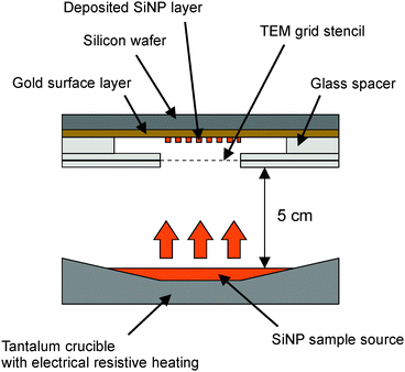
Thin films of patterned arrays of SiNPs were formed by evaporating a suspension of SiNPs in water in an Edwards Auto 306 evaporator system onto gold surfaces freshly deposited upon silicon wafers. The deposition apparatus was arranged as shown in Fig. 1. The source and collecting target were set approximately 5 cm apart and the base pressure during evaporation was kept below 1 × 10⁻⁶ mbar throughout. The experimental set-up prevented direct measurement of the temperature of the heating source temperature however an estimate was gained via an IR pyrometer directed through the chamber viewport onto the glowing sample source. The maximum temperature was found to be approximately 260 °C. Patterned arrays of the nanoparticle material were created by masking the gold film with a row of uncoated copper TEM meshes mounted to glass cover slips. After 1 hour of evaporation at 260 °C the TEM stencils were removed leaving a grid-like pattern comprising an array of approximately 10 × 10![[thin space (1/6-em)]](https://www.rsc.org/images/entities/char_2009.gif) 300 μm2 squares of deposited material on the surface.
300 μm2 squares of deposited material on the surface.
2.3. FTIR mapping
Micro-mapped FTIR spectroscopy on the patterned arrays of SiNP structures was performed using a Vertex 80V FTIR and Hyperion 3000 infrared microscope (Bruker Corp.) on the MIRIAM (Multimode InfraRed Imaging and Microspectroscopy) beamline at the Diamond Light Source, Harwell.52 In order to enhance the signal-to-noise ratio, spectra were taken under grazing incidence conditions. FTIR data acquisition and analysis were performed using Bruker Optik's OPUS software (version 7.0).2.4. Thick film irradiation
Irradiation studies were carried out at beamline D1011 at MAX-lab, Lund. A sample of the amine-terminated SiNPs (approximately 120 μg) was suspended in several drops of water and cast by a pipette onto a freshly sputtered gold foil. The film was transferred into the UHV loadlock to allow the suspending solvent to be pumped away and the sample was irradiated with 150 eV photons as multiple XPS scans were collected over the Si2p core level energy window. The beamspot size at the sample surface was approximately 3 × 10⁻⁶ m2 and the photon flux was 1 × 10¹⁰ photons s−1. Each sweep of this window lasted 90 seconds from which we can estimate the total cumulative radiation dose to be 9 × 10⁹ photons.Periodically throughout the experiment the Au4f signal was collected in order to check and correct for sample charging. All XPS spectra were acquired using a Scienta SES200 electron energy analyzer with an energy resolution, E/dE, of 1.5 × 10³ to 1.3 × 10⁴ running SES analyzer control software. For core level XPS data collection, the analyzer pass energy was set at 150 meV with energy steps of 0.05 eV and a dwell time of 1 second. All measurements were carried out at room temperature in normal emission geometry. XPS data analysis and high-resolution peak fitting were performed with CasaXPS software (version 2.3.15).
3. Results and discussion
A patterned thin film of evaporated SiNPs was formed by evaporating a suspension of SiNP material through a TEM grid onto a cleaned gold substrate so as to create an ordered, discrete array of SiNPs squares, each 300 μm2, through which the surface species could be characterized by microimaging FTIR. Although it was possible to clearly view distinct grid-like patterns of the deposited material by eye, observing the same under microscope conditions presented some challenges and clearly defined transitions between the SiNP film and the underlying substrate were difficult to see. Fig. 2 shows an optical microscope image (at 36× magnification) of the fabricated film surface. The darker regions show where the SiNP film has been deposited. The lower left corner of the area shown in the figure corresponds to the top right corner of a SiNP film square. As can be discerned from the image, any sharp edges that might outline the areas of deposited material are considerably blurred, and the deposits appear to be of varying shapes and thickness. It is possible that localized heating of the target substrate by heat radiation from the hot sample source close by led to surface rearrangements after the SiNP layer was deposited. Solvent drying effects may also play a role in the arrangements of the surface coverage.53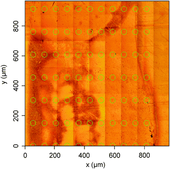 | ||
| Fig. 2 Optical image of the evaporated film surface. The dark areas correspond to regions of deposited material. | ||
Recent SEM studies on evaporation deposition of silver nanoparticles upon Si and Si3N4 surfaces through a single 20 μm diameter aperture have shown that the deposited layer has a much larger diameter as the flow of material diffuses through the aperture and spreads out.54 In the previously cited reference, the spacing between the target surface and the aperture was 0.2 mm and gave a deposited spot with a diameter of 120 μm, a six-fold increase. This spacing is somewhat smaller than used in the work reported here. We estimate the height of the glass spacer between the gold target surface and the TEM stencil to be ∼0.8 mm. This increase in height, in addition interference effects due to the multisource nature of the TEM grid whereby each open hole within the mesh acts as a point source of NP material, will lead to blurring of the deposited features. The lack of well-defined patterns signifies further development is necessary to improve the method. A typical FTIR spectrum from a dark area within the evaporated film (Fig. 3) shows typical resonant features expected for the system under study,51 although oxide signatures are not easily discernible in this case.
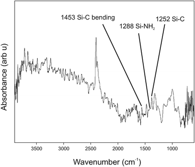 | ||
| Fig. 3 FITR spectrum from a thin film of evaporated SiNPs. The spectral components of interest are labeled in the figure. | ||
Fig. 4 shows the spatially resolved absorption maps over a 1000 × 1000 μm region of the evaporated film. The clear signature of Si–NH2 can be seen in the right panel concentrated within several small islands of material. Likewise for the distribution of silicon oxide and Si–C bonds within the film.
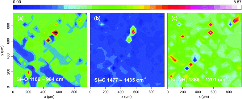 | ||
| Fig. 4 FTIR images of evaporated SiNPs: (right panel) absorption intensity maps over the Si–NH2 band; (left panel) the Si–O band; (middle panel) the Si–C band. | ||
Such islands of material were frequently observed during data collection and ordered distributions of material in clearly recognizable patterns were difficult to discern, as discussed above. Meyer and co-workers observed similar clustering of evaporated material within spots of evaporated silver nanoparticles ever after 240 seconds.54 This suggests refinement is necessary in our film preparation techniques in order to produce a film with sufficiently distinguishable features.
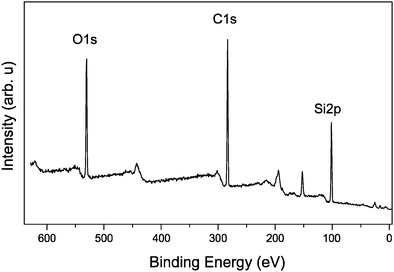
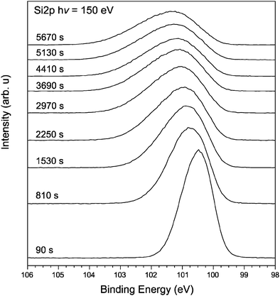
XPS survey spectra from the thin films of amine-terminated SiNPs reveal features expected of the chemical species within the sample (Fig. 5). Strong peaks associated with silicon, carbon and oxygen may be seen. The carbon is a mixture of carbon within the film as well as unavoidable contributions from adventitious hydrocarbons within the UHV system. The presence of oxygen is indicative of some amount of oxidation within the materials. Fig. 6 shows the development of the XPS spectrum over the Si2p region from a thick film of amine-terminated SiNPs during extended exposure to 150 eV photons every 90 seconds up to 5670 seconds corresponding to 63 sweeps of the silicon region. To simplify the figure and aid inspection, only a selection of scans is included in the plot. As can be clearly seen after 90 seconds, the single peak gradually shifts to a higher binding energy decreases in intensity and assumes a broader profile.
In Fig. 7, the first and last spectra from Fig. 6 are compared directly. Both spectra have been fitted with an appropriate number of Gaussian–Lorentzian shaped peaks and the peak positions are indicated within the figure and have been scaled to the same maximum intensity. The initial spectrum after 90 seconds of irradiation shows a peak at 100.53 eV. The binding energy of the Si2p core level is found to be 100.5 eV, which is between the binding energy of Si0 of unoxidized silicon Si–Si (98.7 eV) and Si4+ within SiO2 (103.3 eV).55
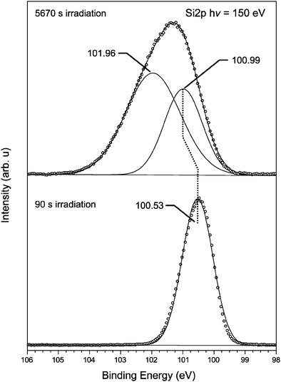 | ||
| Fig. 7 XPS spectra from a film of dropcast amine-terminated SiNPs after 90 seconds and 5670 seconds irradiation with 150 eV photons (lower and upper scans respectively) from Fig. 1. Each spectrum is decomposed into an appropriate number of Gaussian–Lorentzian profile peaks, set upon a Shirley background function. Spectra are presented with the background contribution removed for clarity. | ||
This indicates that the Si charge state within the NPs lies somewhere between 0 and 4+. As the exposure time to the X-ray radiation increases, the Si–Si peak shifts towards a higher binding energy. After 5670 seconds irradiation the peak lies at 100.99 eV as the surface layer has undergone positive charge buildup, and an additional peak is found at 101.96 eV. It is difficult to determine if this latter peak is silicon oxide or silicon carbide although it lies close to the expected binding energy for Si3+ at 101.9 eV56 and Si–C–N bonding.57
The XPS peak shifts can be interpreted in terms of a combination of sample oxidation and charge buildup. The former has been studied previously on similar samples of capped SiNPs.58 The latter is a potentially significant result, since although studies on the actual cytotoxicity of silicon-based NPs are still somewhat rare, recent literature suggests that surface charge and oxidative stress play a role in determining the cellular uptake and cytotoxicity of NPs.53 The exact nature is not yet fully understood with differing findings being reported. Some workers have observed cytotoxic effects in positively-charged gold nanorods,59 while others have observed specific reduced cytotoxicity in cationic nanoparticles.55 Positively-charged amine-terminated SiNPs were found to be more cytotoxic than neutral azide-terminated SiNPs with similar diameters.60 Several studies have shown that capped nanoparticles can become cytotoxic under oxidative and photolytic conditions. For example MAA–tri-n-octylphosphine oxide (MAA–TOPO)-capped CdSe NPs can induce cell death if the NPs are exposed to UV radiation.20 The protective MAATOPO coating was found to be labile, and underwent degradation after 1 hour of UV exposure leading to surface oxidation and release of Cd ions, exposing the toxic coating material and the core to the cells. The concentration of measured Cd continued as UV exposure progressed suggesting the susceptibility of the capping layer to UV light. This is an important result; if amine-terminated SiNPs experience positive charge buildup and so become cytotoxic in X-ray environments this may severely curtail the choice of applications in which they can be used without posing a health risk or introducing unwanted side effects.
4. Conclusions
We have synthesized and studied films of amine-terminated SiNPs by an IR-mapping technique. Nanostencilling via TEM meshes allows the deposition of NP material onto the desired substrate, as detected by FTIR microscopy, but the small size of the NPs compared to that of the TEM grid apertures, and possible substrate heating effects limit the fine detection of well-resolved structures and the material appears in clusters upon the surface. This work demonstrates the potential of the nanostencilling technique for film synthesis, with which further refinement could lead to simple fabrication of arrays for use in nanoscale devices. The evolution of the XPS spectra from thick films of amine-terminated SiNPs under extended irradiation by 150 eV X-ray photons has been studied. As irradiation progresses the films experience charge buildup and an oxide species develops at 101.96 eV. Although the nanoparticles here display robust PL stability in biological environments, this result suggests environments where the nanoparticles might come under exposure to X-ray irradiation, such as in X-ray imaging should be avoided so as to minimize any potential cytotoxic effects.Acknowledgements
This research is supported by EPSRC under grant number EP/G01664X/1 and European Thermodynamics Ltd. The research leading to the XPS results received funding from the European Community's Seventh Framework Programme (FP7/2007–2013) under grant agreement No. 226716 and the assistance and advice of Dr Alexei Preobrajenski (MAX-lab) throughout XPS data collection is gratefully acknowledged. The authors thank Diamond Light Source for access to beamline B22 (proposal number SM7065) that contributed to the FTIR results presented here. Professor Julea Butt (UEA) is thanked for access to the UHV evaporation apparatus. JA is thankful for a Tyndall studentship and an ORS award.Notes and references
- X. Michalet, F. F. Pinaud, L. A. Bentolila, J. M. Tsay, S. Doose, J. J. Li, G. Sundaresan, A. M. Wu, S. S. Gambhir and S. Weiss, Science, 2005, 307, 538–544 CrossRef CAS PubMed.
- N. O'Farrell, A. Houlton and B. R. Horrocks, Int. J. Nanomed., 2006, 1, 451–472 CrossRef CAS.
- M. Tomaselli, J. L. Yarger, M. Bruchez, R. H. Havlin, D. deGraw, A. Pines and A. P. Alivisatos, J. Chem. Phys., 1999, 110, 8861 CrossRef CAS PubMed.
- L. Brus, J. Phys. Chem., 1994, 98, 3575–3581 CrossRef CAS.
- J. D. Holmes, K. J. Ziegler, R. C. Doty, L. E. Pell, K. P. Johnston and B. A. Korgel, J. Am. Chem. Soc., 2001, 123, 3743–3748 CrossRef CAS PubMed.
- S. S. Iyer and Y. H. Xie, Science, 1993, 260, 40–46 CAS.
- P. R. Coxon, Q. Wang and Y. Chao, J. Phys. D: Appl. Phys., 2011, 44, 495301 CrossRef.
- A. G. Cullis, L. T. Canham and P. D. J. Calcott, J. Appl. Phys., 1997, 82, 909 CrossRef CAS PubMed.
- B. Ballou, B. C. Lagerholm, L. A. Ernst, M. P. Bruchez and A. S. Waggoner, Bioconjugate Chem., 2004, 15, 79–86 CrossRef CAS PubMed.
- M. C. Beard, K. P. Knutsen, P. Yu, J. M. Luther, Q. Song, W. K. Metzger, R. J. Ellingson and A. J. Nozik, Nano Lett., 2007, 7, 2506–2512 CrossRef CAS PubMed.
- R. A. Rippel and A. M. Seifalian, J. Nanosci. Nanotechnol., 2011, 11, 3740–3748 CrossRef CAS PubMed.
- A. Fojtik, J. Valenta, I. Pelant, M. Kalal and P. Fiala, J. Mater. Process. Technol., 2007, 181, 88–92 CrossRef CAS PubMed.
- G. Bertin and D. Averbeck, Biochimie, 2006, 88, 1549–1559 CrossRef CAS PubMed.
- Z.-B. Li, W. Cai and X. Chen, J. Nanosci. Nanotechnol., 2007, 7, 2567–2581 CrossRef CAS PubMed.
- L. Zhang, F. X. Gu, J. M. Chan, A. Z. Wang, R. S. Langer and O. C. Farokhzad, Clin. Pharmacol. Ther., 2008, 83, 761–769 CrossRef CAS PubMed.
- S. D. Caruthers, S. A. Wickline and G. M. Lanza, Curr. Opin. Biotechnol., 2007, 18, 26–30 CrossRef CAS PubMed.
- D. A. Giljohann, D. S. Seferos, W. L. Daniel, M. D. Massich, P. C. Patel and C. A. Mirkin, Angew. Chem., Int. Ed., 2010, 49, 3280–3294 CrossRef CAS PubMed.
- S. Tiwari, F. Rana, H. Hanafi, A. Hartstein, E. F. Crabbe and K. Chan, Appl. Phys. Lett., 1996, 68, 1377 CrossRef CAS PubMed.
- W. J. Parak, T. Pellegrino and C. Plank, Nanotechnology, 2005, 16, R9–R25 CrossRef CAS PubMed.
- M. E. Akerman, W. C. W. Chan, P. Laakkonen, S. N. Bhatia and E. Ruoslahti, Proc. Natl. Acad. Sci. U. S. A., 2002, 99, 12617–12621 CrossRef CAS PubMed.
- D. Kim, S. Park, J. H. Lee, Y. Y. Jeong and S. Jon, J. Am. Chem. Soc., 2007, 129, 7661–7665 CrossRef CAS PubMed.
- C.-Y. Jin, B.-S. Zhu, X.-F. Wang and Q.-H. Lu, Chem. Res. Toxicol., 2008, 21, 1871–1877 CrossRef CAS PubMed.
- S. J. Cho, D. Maysinger, M. Jain, B. Röder, S. Hackbarth and F. M. Winnik, Langmuir, 2007, 23, 1974–1980 CrossRef CAS PubMed.
- Z. Lu, C. M. Li, H. Bao, Y. Qiao, Y. Toh and X. Yang, Langmuir, 2008, 24, 5445–5452 CrossRef CAS PubMed.
- A. M. Derfus, W. C. W. Chan and S. N. Bhatia, Nano Lett., 2004, 4, 11–18 CrossRef CAS.
- Q. Wang, Y. Bao, X. Zhang, P. R. Coxon, U. A. Jayasooriya and Y. Chao, Adv. Healthcare Mater., 2012, 1, 189–198 CrossRef CAS PubMed.
- Q. Wang, H. Ni, A. Pietzsch, F. Hennies, Y. Bao and Y. Chao, J. Nanopart. Res., 2011, 13, 405–413 CrossRef CAS.
- F. A. Reboredo and G. Galli, J. Phys. Chem. B, 2005, 109, 1072–1078 CrossRef CAS PubMed.
- A. K. Gupta and M. Gupta, Biomaterials, 2005, 26, 3995–4021 CrossRef CAS PubMed.
- M. Rosso-Vasic, E. Spruijt, B. van Lagen, L. De Cola and H. Zuilhof, Small, 2008, 4, 1835–1841 CrossRef CAS PubMed.
- F. Erogbogbo, K.-T. Yong, I. Roy, G. Xu, P. N. Prasad and M. T. Swihart, ACS Nano, 2008, 2, 873–878 CrossRef CAS PubMed.
- S. Choi and W. L. Murphy, Langmuir, 2008, 24, 6873–6880 CrossRef CAS PubMed.
- P. R. Coxon, M. Newman, M. R. C. Hunt, N. O'Farrell, B. R. Horrocks, N. R. J. Poolton and L. Šiller, J. Appl. Phys., 2012, 111, 054311 CrossRef PubMed.
- J. Nelles, D. Sendor, A. Ebbers, F. M. Petrat, H. Wiggers, C. Schulz and U. Simon, Colloid Polym. Sci., 2007, 285, 729–736 CAS.
- P. K. Sudeep and T. Emrick, ACS Nano, 2009, 3, 4105–4109 CrossRef CAS PubMed.
- F. M. Dickinson, T. A. Alsop, N. Al-Sharif, C. E. M. Berger, H. K. Datta, L. Siller, Y. Chao, E. M. Tuite, A. Houlton and B. R. Horrocks, Analyst, 2008, 133, 1573–1580 RSC.
- D. Haridas, V. Gupta and K. Sreenivas, Bull. Mater. Sci., 2008, 31, 397–400 CrossRef CAS PubMed.
- M. Brust, D. Bethell, C. J. Kiely and D. J. Schiffrin, Langmuir, 1998, 14, 5425–5429 CrossRef CAS.
- B. M. Quinn, C. Dekker and S. G. Lemay, J. Am. Chem. Soc., 2005, 127, 6146–6147 CrossRef CAS PubMed.
- M. Brust, N. Stuhr-Hansen, K. Norgaard, J. B. Christensen, L. K. Nielsen and T. Bjornholm, Nano Lett., 2001, 1, 189–191 CrossRef CAS.
- S. Coe-Sullivan, J. S. Steckel, W.-K. Woo, M. G. Bawendi and V. Bulović, Adv. Funct. Mater., 2005, 15, 1117–1124 CrossRef CAS.
- L. Kim, P. O. Anikeeva, S. A. Coe-Sullivan, J. S. Steckel, M. G. Bawendi and V. Bulović, Nano Lett., 2008, 8, 4513–4517 CrossRef CAS PubMed.
- Y. Chao, L. Siller, S. Krishnamurthy, P. R. Coxon, U. Bangert, M. Gass, L. Kjeldgaard, S. N. Patole, L. H. Lie, N. O'Farrell, T. A. Alsop, A. Houlton and B. R. Horrocks, Nat. Nanotechnol., 2007, 2, 486–489 CrossRef PubMed.
- P. R. Coxon, Y. Chao, B. R. Horrocks, M. Gass, U. Bangert and L. Šiller, J. Appl. Phys., 2008, 104, 084318 CrossRef PubMed.
- P. R. Coxon, S. P. Ashby, M. D. Frogley and Y. Chao, J. Phys. D: Appl. Phys., 2012, 45, 355303 CrossRef.
- F. Klauser, R. Stijepovic, N. Endstrasser, S. Jaksch, N. Memmel and P. Scheier, Surf. Sci., 2009, 603, 2999–3004 CrossRef CAS PubMed.
- A. Colder, F. Huisken, E. Trave, G. Ledoux, O. Guillois, C. Reynaud, H. Hofmeister and E. Pippel, Nanotechnology, 2004, 15, L1–L4 CrossRef CAS.
- J.-H. Park, L. Gu, G. von Maltzahn, E. Ruoslahti, S. N. Bhatia and M. J. Sailor, Nat. Mater., 2009, 8, 331–336 CrossRef CAS PubMed.
- T. J. Brunner, P. Wick, P. Manser, P. Spohn, R. N. Grass, L. K. Limbach, A. Bruinink and W. J. Stark, Environ. Sci. Technol., 2006, 40, 4374–4381 CrossRef CAS.
- W. Lin, Y.-W. Huang, X.-D. Zhou and Y. Ma, Toxicol. Appl. Pharmacol., 2006, 217, 252–259 CrossRef CAS PubMed.
- J. H. Ahire, Q. Wang, P. R. Coxon, G. Malhotra, R. Brydson, R. Chen and Y. Chao, ACS Appl. Mater. Interfaces, 2012, 4, 3285–3292 CAS.
- M. C. Martin, U. Schade, P. Lerch and P. Dumas, TrAC, Trends Anal. Chem., 2010, 29, 453–463 CrossRef CAS PubMed.
- S. Bhattacharjee, L. H. J. de Haan, N. M. Evers, X. Jiang, A. T. M. Marcelis, H. Zuilhof, I. M. C. M. Rietjens and G. M. Alink, Part. Fibre Toxicol., 2010, 7, 25 CrossRef PubMed.
- R. Meyer, S. Hamann, M. Ehmann, D. Konig, S. Thienhaus, A. Savan and A. Ludwig, J. Microelectromech. Syst., 2011, 20, 21–27 CrossRef CAS.
- K. Gupta, V. P. Singh, R. K. Kurupati, A. Mann, M. Ganguli, Y. K. Gupta, Y. Singh, K. Saleem, S. Pasha and S. Maiti, J. Controlled Release, 2009, 134, 47–54 CrossRef CAS PubMed.
- A. V. Boryakov, D. E. Nikolitchev, D. I. Tetelbaum, A. I. Belov, A. V. Ershov and A. N. Mikhaylov, Phys. Solid State, 2012, 54, 394–403 CrossRef CAS.
- W. L. Li, Z. G. Zhang, J. L. Yang and W. D. Fei, Vacuum, 2011, 86, 457–460 CrossRef CAS PubMed.
- Y. Chao, S. Krishnamurthy, M. Montalti, L. Lie, A. Houlton, B. Horrocks, L. Kjeldgaard, V. Dhanak, M. Hunt and L. Šiller, J. Appl. Phys., 2005, 98, 044316 CrossRef PubMed.
- T. S. Hauck, A. A. Ghazani and W. C. W. Chan, Small, 2008, 4, 153–159 CrossRef CAS PubMed.
- L. Ruizendaal, S. Bhattacharjee, K. Pournazari, M. Rosso-Vasic, L. H. J. de Haan, G. M. Alink, A. T. M. Marcelis and H. Zuilhof, Nanotoxicology, 2009, 3, 339–347 CrossRef CAS.
| This journal is © the Owner Societies 2014 |

