 Open Access Article
 This Open Access Article is licensed under a Creative Commons Attribution-Non Commercial 3.0 Unported Licence
Photoexcited carrier dynamics of double-layered CdS/CdSe quantum dot sensitized solar cells measured by heterodyne transient grating and transient absorption methods
N.
Osada
ab,
T.
Oshima
b,
S.
Kuwahara
a,
T.
Toyoda
bc,
Q.
Shen
*bc and
K.
Katayama
*a
aDepartment of Applied Chemistry, Chuo University, 1-13-27, Kasuga, Bunkyo, Tokyo 112-8551, Japan. E-mail: kkata@kc.chuo-u.ac.jp; Fax: +81-3-3817-1913; Tel: +81-3-3817-1913
bDepartment of Engineering Science, The University of Electro-Communications, 1-4-1 Chofugaoka, Chofu, Tokyo 182-8585, Japan. E-mail: shen@pc.uec.ac.jp
cCREST, Japan Science and Technology Agency (JST), 4-1-8 Honcho Kawaguchi, Saitama 332-0012, Japan
First published on 10th January 2014
Abstract
The charge dynamics in the double-layered quantum dot sensitized solar cell (QDSSC) was studied to clarify the reason why the cell performance was much improved by a double-layer coating, by using the heterodyne transient grating (HD-TG) and transient absorption methods, based on a previous study for a conventional QDSSC (N. Maeda et al., Phys. Chem. Chem. Phys., 2013, 15, 11006.) In the double-layered QDSSC, the layer order of CdS and CdSe affected the cell performance. When CdS is in between TiO2 and CdSe, the conversion efficiency was enhanced by 70%, while it was lowered by 50% in the opposite order. From the information on charge dynamics, it was found that electrons were efficiently injected to TiO2 by appropriate band alignment of CdS and CdSe, while only a part of the electrons were transferred to the TiO2 when the layer order was opposite. Furthermore, the reverse electron transfer does not matter for the conversion efficiency, because the process increased even for the appropriate layer order.
Introduction
In the last ten years, the conversion efficiency of quantum dot sensitized solar cells (QDSSCs) showed drastic improvement. QD have properties appropriate for light harvesting applications such as tunable optical absorption by size control and high efficiency multiple exciton generation (MEG).1–3 The theoretical efficiency is as high as 44%, higher than that for dye-sensitized solar cells (DSSCs).4 Furthermore, from a manufacturing viewpoint, the production cost is expected to be much cheaper due to abundant inorganic materials. However, the conversion efficiency at the moment is still lower than that for DSSCs,5–7 although it has been greatly improved in the last few years to nearly 7%,8,9 and much efforts have been made on the QD size,10,11 the core–shell structure of QDs,9,12 surface fabrication and passivation,11,13,14 and semiconductors and substrates,6,15,16 and their optimal combinations.17As a promising effort, mixing of different kinds of QDs as a sensitizer has been reported in recent years. It was first reported by Hodes et al., and the composition of the QD layer was studied carefully.18 The blend of QDs helps the electrons flow smoothly by tuning the band position alignment19,20 and also expanding the absorption wavelength region for light harvesting. Lee et al.20 clarified by ultraviolet photoelectron spectroscopy that the band position of CdSe shifted upwards when a CdS layer was in-between TiO2 and CdSe. The charge transfer between the CdS/CdSe QDs and TiO2 was studied by photoluminescence dynamics, which indicated smooth charge transfer by co-sensitizing CdS and CdSe on TiO2.21 This blend electrode was also used for sensitization of nanotubes,22–24 and hierarchical TiO225 for hydrogen evolution at the counter electrode.19 Recently, Zhong et al. prepared a well-ordered core–shell structure of CdS–CdSe QDs and reached 5.32% conversion efficiency,12 and Kamat et al. demonstrated a Mn-doped CdS/CdSe QDSSC and reached 5.42% efficiency.26 The long-lived exciton for CdSe/CdS QDs was studied from a fundamental viewpoint for utilization of photoexcited carriers.27,28
There is another approach for improving the conversion efficiency, by understanding the mechanism of charge dynamics, typically by using the transient absorption (TA) method. The materials or their combination were modified based on the mechanism information to enhance the injection efficiency and to reduce recombination probabilities. In this field, Hodes et al.29 reviewed the charge processes as compared to those for DSSCs and Kamat et al.1,10,30 studied the initial charge injection process by the TA method and explained it with the Gibbs energy of the QDs and the conduction band of the semiconductor; Shen and Gomez et al.,31–33 studied not only electron but also hole dynamics on the order of picoseconds, which clarified the hole transfer to the electrolyte species.
On the other hand, we have developed a combination methodology of heterodyne transient grating (HD-TG), TA, and transient photocurrent (TP) methods measured in a wide time range from nanoseconds to seconds, and we have studied the charge carrier dynamic in DSSCs34 and QDSSCs35 to improve the conversion efficiency. The difference of our methodology is that we could monitor not only the electrons or holes on the electrode side, but also the dynamics of the redox or electrolyte species on the liquid side at the interface. This is possible because the HD-TG technique we have developed measures the refractive index change, which is very sensitive to dipole change, and thus the charged species at the interface was sensitively monitored. By combination with the TA method, we could get the whole information on charge carriers in the solid, interface, liquid side.
In a previous paper, we showed the dependence on pump intensity, applied bias, electrolyte, for the CdSe QDSSC, and the observed dynamics was assigned from the nanosecond to second order. Furthermore, the effect of ZnS coating was investigated, and optimal coating conditions were proposed by observation of the electron/electrolyte recombination and electron dynamics in TiO235 In this study, we studied the charge dynamics in CdSe/CdS QDSSCs, and clarified why the conversion efficiency was improved by double-layer coating.
Experimental
The method for preparation of the working electrodes was reported in a previous paper.36 Anatase TiO2 paste was prepared by mixing TiO2 nanoparticles with an average diameter of 15 nm (3.0 g), polyethylene glycol with molecular weight of 500![[thin space (1/6-em)]](https://www.rsc.org/images/entities/char_2009.gif) 000 (1.2 g), acetyl acetone (1.0 mL) and water (10 mL) with a mortar for 30 min. The resulting paste was cast onto a glass substrate coated with fluorine doped tin oxide (FTO, 10 Ω, Asahi Glass) with a Scotch tape as a frame and spacer, raking off the excess solution with a glass rod. (Squeegee technique) The TiO2 electrodes were dried in air at room temperature for 10 min, and annealed at 450 °C for 30 min in a furnace, and then cooled down to rt. The film thickness was around 7 ± 1 μm.
000 (1.2 g), acetyl acetone (1.0 mL) and water (10 mL) with a mortar for 30 min. The resulting paste was cast onto a glass substrate coated with fluorine doped tin oxide (FTO, 10 Ω, Asahi Glass) with a Scotch tape as a frame and spacer, raking off the excess solution with a glass rod. (Squeegee technique) The TiO2 electrodes were dried in air at room temperature for 10 min, and annealed at 450 °C for 30 min in a furnace, and then cooled down to rt. The film thickness was around 7 ± 1 μm.
CdS37 and CdSe38 were grown with the chemical bath deposition (CBD) method. A TiO2 electrode was immersed in a mixture solution of CdCl2 (20 mM), NH4Cl (66 mM), NH3 (230 mM), H2NCSNH2 (140 mM) for 40 min for the CdS QDs deposition. For the CdSe QDs deposition, an electrode was immersed in a mixture of CdSO4 (27 mM), N(CH2COONa)3 (40 mM), Na2SeSO3 (27 mM) solution. A TiO2 electrode with CdS QDs was immersed for 6 h, and a bare TiO2 electrode was immersed for 24 h. Zinc sulfide (ZnS) was coated by the SILAR method.39 The electrodes were soaked in (CH3COO)2Zn (0.1 M) and Na2S (0.1 M) solutions in turns with two cycles. A polysulfide solution was used as electrolyte solution with S and Na2S concentrations of 1 M.40 Cu2S was used as a counter electrode.
The principle and the setup of the HD-TG method were reported in detail in previous papers.34,41,42 In this study, the pump light source was an OPO (Surelite II – 10FP) output excited by a Nd:YAG laser (Panther, Continuum, Electro-Optics Inc.), and the pulse light had a wavelength of 570 nm, a pulse width of 5 ns, and a repetition rate of 0.5 Hz. The repetition rate was decided uponas being slow enough to recover the original baseline for the HD-TG and TA measurements. The pump intensity was 0.65 mJ per pulse. The probe light was a fiber coupled CW semiconductor laser with a wavelength of 658 nm for all HD-TG (10 mW) and TA measurements (4 mW). The pump and probe lights were incident from the FTO substrate side to avoid absorption of the pump light by polysulfide redox solution. TA responses were measured at the same probe wavelength just by removing a glass plate of transmission grating used for the HD-TG measurement.
The photoacoustic (PA) spectrum was measured with a home-built apparatus, and the measured wavelength range was 270–900 nm.43 The I–V curves were measured under A.M.1.5 for the area of 0.24 cm2 by a solar simulator (Peccell:PEC-L10). IPCE was measured using home-built IPCE equipment (0.8–1 mW cm−2 for monochromic light).
Results and discussions
We prepared different types of electrodes, TiO2 only, CdSe/TiO2, CdS/TiO2, CdSe/CdS/TiO2, CdS/CdSe/TiO2 electrodes. To confirm the growth of QDs and the band gap energy for the electrodes, PA spectra were measured for them, and the results are shown in Fig. 1. As we expected, the absorption region was extended to 1.75 eV for the CdSe/TiO2, CdSe/CdS/TiO2, CdS/CdSe/TiO2 electrodes mostly due to the absorption of CdSe QDs and no difference was observed for the three electrodes. A small absorption increase was observed for the CdS/TiO2 electrode as compared to the TiO2 only electrode. Based on the effective mass approximation, the average size of CdSe QDs was 7 nm. (Bulk band gap: 1.75 eV, electron and hole mass: 1.18 × 10⁻³¹ and 4 × 10⁻³¹ kg for CdSe were used.)44 | ||
| Fig. 1 PA spectra for the electrodes; TiO2 only, CdSe/TiO2, CdS/TiO2, CdSe/CdS/TiO2, CdS/CdSe/TiO2 electrodes. | ||
Next, IPCE was measured for the electrodes (Fig. 2). As we expected, the energy range was extended only to 2.2 eV for the CdS/TiO2 electrode. The energy regions of the IPCE for the CdSe/TiO2, CdSe/CdS/TiO2, CdS/CdSe/TiO2 electrodes were similar, but IPCE intensity was drastically changed by the presence and the layer order of CdS and CdSe. When the CdS layer was in between TiO2 and CdSe, IPCE was enhanced by about 30% as compared to the CdSe/TiO2 electrode, while it was lowered by about 40% when the CdS layer was on top of the electrode.
 | ||
| Fig. 2 IPCE spectra for the electrodes; TiO2 only, CdSe/TiO2, CdS/TiO2, CdSe/CdS/TiO2, CdS/CdSe/TiO2 electrodes. | ||
The I–V curves for the electrodes were measured and the result is shown in Fig. 3. Similar to the IPCE result, the I–V characteristic was slightly improved in the presence of CdS QDs as compared to a bare TiO2 electrode, and considerably improved in the presence of CdSe QDs, reaching a conversion efficiency of 2.1%. By mixing the CdS and CdSe, the result was influenced by the order of CdS and CdSe coating. When the CdS QDs were in between CdSe and TiO2, both the Jsc and Voc were improved, and the conversion efficiency was improved by 70% as compared to the CdSe only, while the opposite tendency was observed when the CdS QDs were on top of the layer, and the efficiency became almost half of the CdSe only.
 | ||
| Fig. 3 I–V curves for the electrodes; TiO2 only, CdSe/TiO2, CdS/TiO2, CdSe/CdS/TiO2, CdS/CdSe/TiO2 electrodes, and their I–V characteristics. | ||
To study how the combination of CdSe and CdS affected the conversion efficiency, we studied the charge dynamics by TA and HD-TG measurements. The pump wavelength for these measurements was selected at 570 nm to selectively excite the CdSe QDs.
The TA responses for the CdSe/TiO2, CdSe/CdS/TiO2, CdS/CdSe/TiO2 electrodes are shown in Fig. 4. As we have already assigned, the dynamics consisted of the decay of trapped electrons in TiO2 in the 1–100 ms region and the long lasting decay from μs–100 ms corresponding to the inhomogeneously distributed conduction electrons in TiO2.35,45 For the CdSe/CdS/TiO2 electrode, the trapped electrons were considerably increased as compared to the CdSe/TiO2 electrode, while they decreased for the CdS/CdSe/TiO2 electrode. It means that the electrons were effectively accumulated in TiO2 for the former electrode, but they were lost for the latter one.
 | ||
| Fig. 4 TA responses for CdSe/TiO2, CdSe/CdS/TiO2, CdS/CdSe/TiO2 electrodes. The pump wavelength was 570 nm. | ||
Next, HD-TG measurements were performed for the CdSe/TiO2, CdSe/CdS/TiO2, CdS/CdSe/TiO2 electrodes (Fig. 5). In the HD-TG responses for a QDSSC electrode, we can observe reorganization of the ionic species at the interface in 1–100 μs, a thermal response in 0.1–1 ms, and reverse electron transfer to redox species in 1–100 ms.35 Since the thermal response does not matter in the process of charge dynamics, the 1st and 3rd components were considered. A scheme corresponding to the band alignment of CdSe, CdS and TiO2 is shown in Scheme 1 to understand the charge dynamics.19,20 As compared to the CdSe/TiO2 electrode, the 1st component was delayed and the 3rd component increased a little in its intensity for the CdSe/CdS/TiO2 electrode. In the case of the CdS/CdSe/TiO2 electrode, the 1st component was delayed and the 3rd component completely disappeared. It was unexpected because the electrode with lower conversion efficiency showed a smaller amount of the electrons which were subject to reverse electron transfer. For the CdSe/CdS/TiO2 electrode, it is considered that the electrons were efficiently injected into TiO2, which was supported by the fact of the increase in the accumulated electrons in TiO2 from the TA result, and that more electrons were subject to reverse electron transfer. For the CdS/CdSe/TiO2 electrode, based on Scheme 1, this can be explained with two possible reasons; (1) the band alignment suggests that only a part of the electrons were injected into TiO2, while the other part of the electrons moved to the CdS side. The TA result supports the decrease in the amount of accumulated electrons into TiO2. The amount of reverse electron transfer was decreased because of the decrease in the accumulated electrons in TiO2. (2) The generated holes in CdSe were difficult to move to the CdS side because of the energy barrier, and the holes were confined in the CdSe layer. The higher density of the holes in CdSe caused recombination with the electrons in TiO2. It is likely that the second reason would be true because, if the 1st reason were true, some part of the electrons would still be subjected to the reverse electron transfer process, which would give some signal intensity for the 3rd HD-TG component. For both electrodes, the 1st component was delayed because the double semiconductor layers screened effectively the Coulomb force of the electrons in TiO2, which caused the motion of ionic species to slow down.
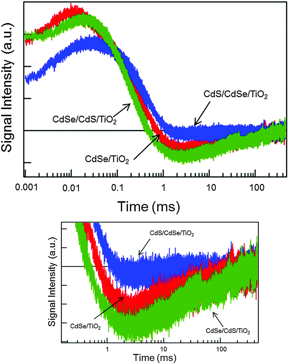 | ||
| Fig. 5 HD-TG responses for the CdSe/TiO2, CdSe/CdS/TiO2, CdS/CdSe/TiO2 electrodes. The pump wavelength was 570 nm. The bottom figure is the expansion in the 1–100 ms range. | ||
 | ||
| Scheme 1 Band alignment of CdSe/TiO2, CdSe/CdS/TiO2, CdS/CdSe/TiO2 electrodes. The arrow from the TiO2 conduction band indicates back electron transfer or recombination processes. | ||
Conclusions
We could confirm improvement of the QDSSCs by using the double layer of CdSe and CdS QDs, and the order of the coating was important; only when the CdS layer was in-between the TiO2 and CdSe QDs, the IPCE, the I–V characteristic and the conversion efficiency were improved, while they decreased when the CdS layer was on the top of the electrode. This reason was studied with charge dynamics measurements and TA and HD-TG methods. It was clarified that due to the appropriate band alignment for the CdSe/CdS/TiO2 electrode, the injected electrons were smoothly transferred to TiO2 and accumulated there, and reverse electron transfer did not matter for the efficiency.References
- P. V. Kamat, J. Phys. Chem. C, 2008, 112, 18737–18753 CAS.
- S. Ruhle, M. Shalom and A. Zaban, ChemPhysChem, 2010, 11, 2290–2304 CrossRef PubMed.
- Q. Shen, K. Katayama, T. Sawada, S. Hachiya and T. Toyoda, Chem. Phys. Lett., 2012, 542, 89–93 CrossRef CAS PubMed.
- M. C. Hanna and A. J. Nozik, J. Appl. Phys., 2006, 100, 074510–074518 CrossRef PubMed.
- Q. X. Zhang, X. Z. Guo, X. M. Huang, S. Q. Huang, D. M. Li, Y. H. Luo, Q. Shen, T. Toyoda and Q. B. Meng, Phys. Chem. Chem. Phys., 2011, 13, 4659–4667 RSC.
- S. Q. Huang, Q. X. Zhang, X. M. Huang, X. Z. Guo, M. H. Deng, D. M. Li, Y. H. Luo, Q. Shen, T. Toyoda and Q. B. Meng, Nanotechnology, 2010, 21, 1–7 Search PubMed.
- Q. Shen, A. Yamada, S. Tamura and T. Toyoda, Appl. Phys. Lett., 2010, 97, 123107 CrossRef PubMed.
- Z. Pan, K. Zhao, J. Wang, H. Zhang, Y. Feng and X. Zhong, ACS Nano, 2013, 7, 5215–5222 CrossRef CAS PubMed.
- J. Wang, I. Mora-Seró, Z. Pan, K. Zhao, H. Zhang, Y. Feng, G. Yang, X. Zhong and J. Bisquert, J. Am. Chem. Soc., 2013, 135, 15913–15922 CrossRef CAS PubMed.
- I. Robel, M. Kuno and P. V. Kamat, J. Am. Chem. Soc., 2007, 129, 4136–4137 CrossRef CAS PubMed.
- H. Zhang, K. Cheng, Y. M. Hou, Z. Fang, Z. X. Pan, W. J. Wu, J. L. Hua and X. H. Zhong, Chem. Commun., 2012, 48, 11235–11237 RSC.
- Z. Pan, H. Zhang, K. Cheng, Y. Hou, J. Hua and X. Zhong, ACS Nano, 2012, 6, 3982–3991 CrossRef CAS PubMed.
- I. Mora-Sero, S. Gimenez, F. Fabregat-Santiago, R. Gomez, Q. Shen, T. Toyoda and J. Bisquert, Acc. Chem. Res., 2009, 42, 1848–1857 CrossRef CAS PubMed.
- T. Toyoda and Q. Shen, J. Phys. Chem. Lett., 2012, 3, 1885–1893 CrossRef CAS.
- L. J. Diguna, Q. Shen, J. Kobayashi and T. Toyoda, Appl. Phys. Lett., 2007, 91, 023116 CrossRef PubMed.
- M. Samadpour, S. Gimenez, P. P. Boix, Q. Shen, M. E. Calvo, N. Taghavinia, A. I. Zad, T. Toyoda, H. Miguez and I. Mora-Sero, Electrochim. Acta, 2012, 75, 139–147 CrossRef CAS PubMed.
- I. Mora-Sero, S. Gimenez, F. Fabregat-Santiago, R. Gomez, Q. Shen, T. Toyoda and J. Bisquert, Acc. Chem. Res., 2009, 42, 1848–1857 CrossRef CAS PubMed.
- O. Niitsoo, S. K. Sarkar, C. Pejoux, S. Rühle, D. Cahen and G. Hodes, J. Photochem. Photobiol., A, 2006, 181, 306–313 CrossRef CAS PubMed.
- Y.-L. Lee, C.-F. Chi and S.-Y. Liau, Chem. Mater., 2009, 22, 922–927 CrossRef.
- C.-F. Chi, H.-W. Cho, H. Teng, C.-Y. Chuang, Y.-M. Chang, Y.-J. Hsu and Y.-L. Lee, Appl. Phys. Lett., 2011, 98, 012101 CrossRef PubMed.
- K.-H. Lin, C.-Y. Chuang, Y.-Y. Lee, F.-C. Li, Y.-M. Chang, I. P. Liu, S.-C. Chou and Y.-L. Lee, J. Phys. Chem. C, 2011, 116, 1550–1555 Search PubMed.
- S. Cheng, W. Fu, H. Yang, L. Zhang, J. Ma, H. Zhao, M. Sun and L. Yang, J. Phys. Chem. C, 2011, 116, 2615–2621 Search PubMed.
- X. F. Gao, W. T. Sun, G. Ai and L. M. Peng, Appl. Phys. Lett., 2010, 96, 153104 CrossRef PubMed.
- X. Yin, W. Que, D. Fei, H. Xie, Z. He and G. Wang, Electrochim. Acta, 2013, 89, 561–570 CrossRef CAS PubMed.
- X.-Y. Yu, J.-Y. Liao, K.-Q. Qiu, D.-B. Kuang and C.-Y. Su, ACS Nano, 2011, 5, 9494–9500 CrossRef CAS PubMed.
- P. K. Santra and P. V. Kamat, J. Am. Chem. Soc., 2012, 134, 2508–2511 CrossRef CAS PubMed.
- G. Rainò, I. Moreels, A. Hassinen, T. Stöferle, Z. Hens and R. F. Mahrt, Nano Lett., 2012, 12, 5224–5229 CrossRef PubMed.
- K. Wu, W. E. Rodríguez-Córdoba, Z. Liu, H. Zhu and T. Lian, ACS Nano, 2013, 7, 7173–7185 CrossRef CAS PubMed.
- G. Hodes, J. Phys. Chem. C, 2008, 112, 17778–17787 CAS.
- A. Kongkanand, K. Tvrdy, K. Takechi, M. Kuno and P. V. Kamat, J. Am. Chem. Soc., 2008, 130, 4007–4015 CrossRef CAS PubMed.
- N. Guijarro, T. Lana-Villarreal, Q. Shen, T. Toyoda and R. Gomez, J. Phys. Chem. C, 2010, 114, 21928–21937 CAS.
- N. Guijarro, Q. Shen, S. Gimenez, I. Mora-Sero, J. Bisquert, T. Lana-Villarreal, T. Toyoda and R. Gomez, J. Phys. Chem. C, 2010, 114, 22352–22360 CAS.
- Q. Shen, Y. Ayuzawa, K. Katayama, T. Sawada and T. Toyoda, Appl. Phys. Lett., 2010, 97, 263113 CrossRef PubMed.
- S. Kuwahara, H. Hata, S. Taya, N. Maeda, Q. Shen, T. Toyoda and K. Katayama, Phys. Chem. Chem. Phys., 2013, 15, 5975–5981 RSC.
- N. Maeda, H. Hata, N. Osada, Q. Shen, T. Toyoda, S. Kuwahara and K. Katayama, Phys. Chem. Chem. Phys., 2013, 15, 11006–11013 RSC.
- Q. Shen and T. Toyoda, Thin Solid Films, 2003, 438–439, 167–170 CrossRef CAS.
- R. Jayakrishnan, P. N. Jaya, K. Beena Annie, S. K. Kulkarni and R. K. Pandey, Semicond. Sci. Technol., 1996, 11, 116 CrossRef CAS.
- S. Gorer and G. Hodes, J. Phys. Chem., 1994, 98, 5338–5346 CrossRef CAS.
- S.-m. Yang, C.-h. Huang, J. Zhai, Z.-s. Wang and L. Jiang, J. Mater. Chem., 2002, 12, 1459–1464 RSC.
- Y. Tachibana, H. Y. Akiyama, Y. Ohtsuka, T. Torimoto and S. Kuwabata, Chem. Lett., 2007, 36, 88–89 CrossRef CAS.
- K. Katayama, M. Yamaguchi and T. Sawada, Appl. Phys. Lett., 2003, 82, 2775–2777 CrossRef CAS PubMed.
- M. Yamaguchi, K. Katayama and T. Sawada, Chem. Phys. Lett., 2003, 377, 589–594 CrossRef CAS.
- A. Rosencwaig and A. Gersho, J. Appl. Phys., 1976, 47, 64–69 CrossRef PubMed.
- S. Nomura and T. Kobayashi, Solid State Commun., 1991, 78, 677–680 CrossRef CAS.
- T. Zewdu, J. N. Clifford, J. P. Hernandez and E. Palomares, Energy Environ. Sci., 2011, 4, 4633–4638 CAS.
| This journal is © the Owner Societies 2014 |