 Open Access Article
 This Open Access Article is licensed under a
 Creative Commons Attribution 3.0 Unported Licence
Optical near-field excitation at commercial scanning probe microscopy tips: a theoretical and experimental investigation
Christoph
Huber
ac,
Andreas
Trügler
b,
Ulrich
Hohenester
b,
Yehiam
Prior
c and
Wolfgang
Kautek
*a
aDepartment of Physical Chemistry, University of Vienna, Währinger Strasse 42, A-1090 Vienna, Austria. E-mail: wolfgang.kautek@univie.ac.at; Tel: +43 1 4277 52470
bDepartment of Physics, Karl-Franzens-University Graz, Universitätsplatz 5, A-8010 Graz, Austria. E-mail: ulrich.hohenester@uni-graz.at; Tel: +43 316 380 5227
cDepartment of Chemical Physics, The Weizmann Institute of Science, Rehovot, 76100 Israel. E-mail: Yehiam.Prior@weizmann.ac.il; Tel: +972 8 934 4008
First published on 13th September 2013
Abstract
A systematic study of the influence of the excitation angle, the light polarization and the coating thickness of commercial SPM tips on the field enhancement in an apertureless scanning near-field optical microscope is presented. A new method to optimize the alignment of the electric field vector along the major tip axis by measuring the resonance frequency was developed. The simulations were performed with a MNPBEM toolbox based on the Boundary Element Method (BEM). The influence of the coating thickness was investigated for the first time. Coatings below 40 nm showed a drastic influence both on the resonance wavelength and the enhancement. A shift to higher angles of incidence for the maximum enhancement could be observed for greater tip radii.
1. Introduction
In optical nanolithography, the dependence of the Abbe diffraction limit on the laser wavelength can be overcome by the application of apertureless near-field microscopes1–7 where a laser-illuminated tip is located at a nanometre distance from a substrate. The achievable resolution is in the order of the radius of curvature of the tip (<10 nm).2,8 Extremely high field enhancements of up to 103 can be realized due to antenna effects, geometrical singularities, and surface plasmon resonances. A further well known application is the tip-enhanced Raman spectroscopy (TERS).9–15 Values of up to 106 often mentioned for Raman measurements12,16–18 are due to inconsistent definitions of the field enhancement factor.19Rough estimations consider a simple dipole–dipole model. However, for a full description of a tip–sample system this approach is not sufficient because this model does not incorporate retardation or multipole effects. Theoretical investigations have to go beyond the analytical solution provided by the Mie theory by fully simulating Maxwell equations when more complex structures should be described. A considerable number of various methods to solve tip–substrate interactions can be found. Examples include the finite difference time domain method (FDTD),20–23 the method of moments,24 the generalized field propagator technique,25,26 the multiple multipole method (MMP),14,27,28 the Green's function method,29 the finite element method (FEM),30 and also the boundary element method.31,32
In this work, a systematic study on the influence of geometrical and illumination parameters of SPM tips is presented. The original motivation was the design and development of an apertureless scanning near-field microscope based on a high-power fs-laser oscillator as a beam source, which can be used for surface modification beyond the diffraction limit of light. We employed a Matlab Toolbox33 based on the boundary element method34 due to its low computational demand and thus its ability to provide prompt results even on a desktop workstation. The influence of various experimental parameters like excitation angle, light polarization and coating thickness was evaluated, theoretically and experimentally. The influence of the laser polarization was studied with a newly developed method adaptive for the fine tuning of the polarization angle for light lever based SPM-systems. Furthermore it could be shown that the metal coating thickness on SPM-tips strongly determines high field enhancements.
2. Theory and experiment
2.1 Boundary element method (BEM)
The boundary element method is a flexible and accurate technique for the calculation of the electromagnetic properties of arbitrarily shaped metallic nanoparticles described by an isotropic dielectric function and abrupt particle interfaces. In contrast to the other methods mentioned above, in the BEM only the surface of the corresponding structure needs to be discretised. In the approach of García de Abajo and Howie34 one uses as basic quantities the scalar and vector potentials Φ and A rather than the electric and magnetic fields E and H. For external excitations Φext and Aext the solutions for the potentials in the corresponding medium can be expressed as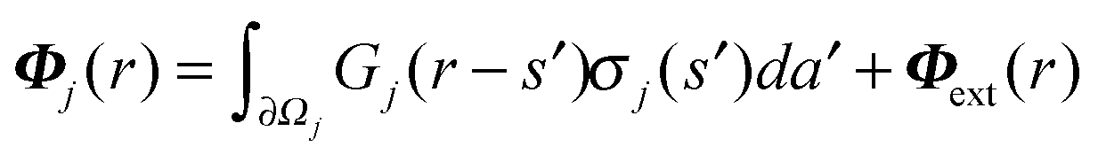 | (1a) |
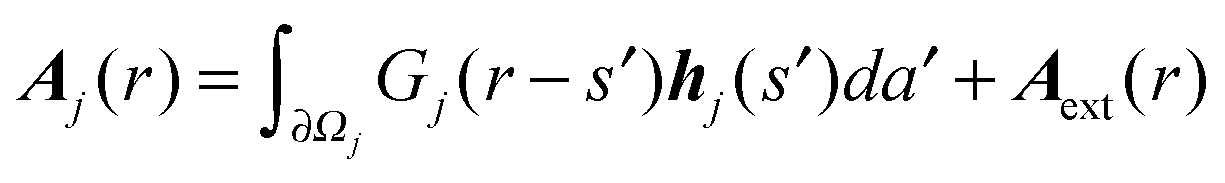 | (1b) |
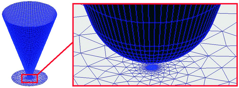 | ||
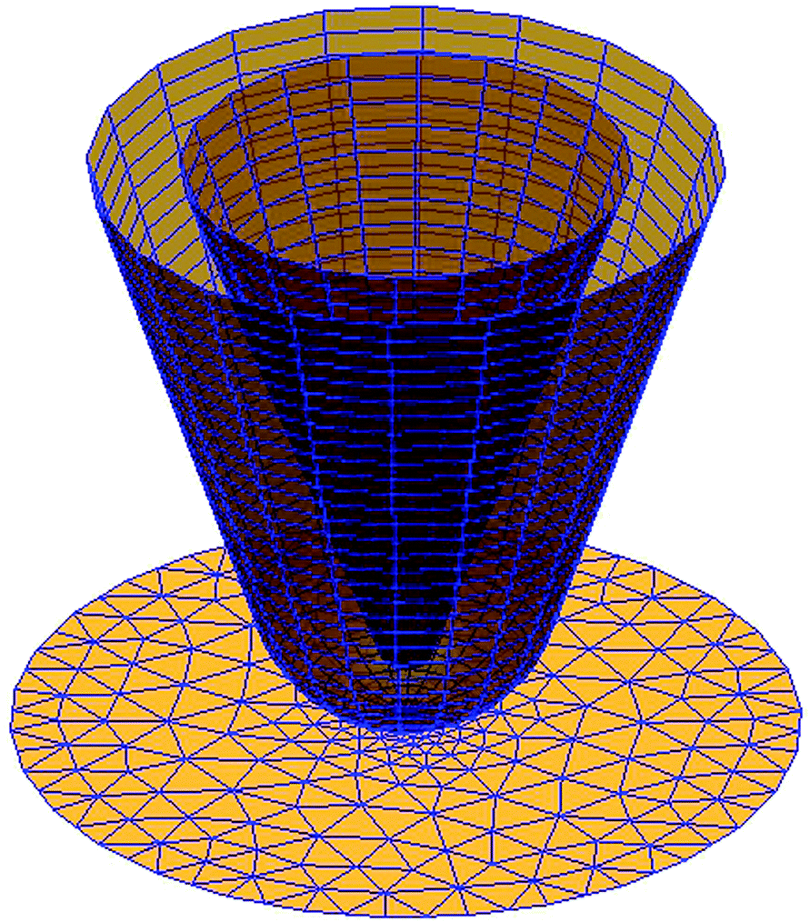
| Fig. 1 Geometrical structure and mesh of the used boundary element model for the calculation of the field enhancement factors. The radius of curvature is 10 nm and the average element size is 30 nm2. | ||
To account for the reflected waves at the substrate underneath the tip, we incorporate this part into the whole excitation process through the Fresnel reflection coefficient35 for TM-waves
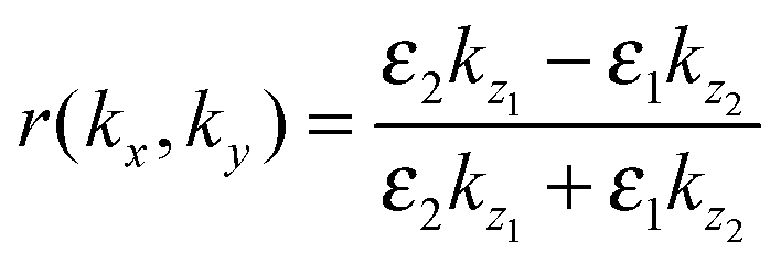 | (2) |
2.2 Numerical tip–substrate model
The geometric model for the simulation is based on a tapered tip with a hemispherical endcap located over a disk-shaped substrate. The laser illuminates the tip from the side to guarantee minor limitations on the available substrates. In the simulations, we assumed a plane wave excitation that illuminates the whole tip–sample system from one direction under a certain angle. The dielectric properties of the tip, the substrate, and the background can be selected independently; the values for gold and silicon were taken from tabulated data.36The discretisation was chosen in such a way that areas of high gradients, like the end of the tip or the surface underneath the tip provided an element size below 0.1 nm2, whereas the mean element size was about 30–35 nm2 (Fig. 1). It is obvious that the highest gradients are expected directly underneath the tip; therefore the highest element density was located there and a variation of the disk-diameter had no significant influence on the results of interest.
In all calculations, the full Maxwell equations have been solved, including retardation and multipole effects.
2.3 Experimental apertureless scanning near-field optical microscope setup
The excitation laser used in the experiments was a Ti:sapphire oscillator (Micra-5, Coherent) with a tuneable bandwidth of 30–100 nm, a repetition rate of 82 MHz, a pulse energy of 6 nJ, and a pulse length of 60 fs. The commercial SPM (XE 120, Park System) was mounted on top of an inverted microscope (Eclipse TE2000-U, Olympus). The xy-scanner was spatially separated from the z-scanner for crosstalk elimination. Silicon tips without coating (AC160-TS, Olympus) and coated with 60 nm gold (ATEC-NC-Au, NanoWorld AG) were used.The tip is illuminated from the side under an angle of 76 degrees from the major tip axis (Fig. 2). The polarization of light was defined relative to the major tip axis. p-polarized light meant alignment of the electric field vector at an angle of 0° relative to the major tip axis. Alignment was performed using two CCD cameras. One camera was positioned on the top and the other one at the bottom, in the inverted microscope. The design of the used SPM tips (Fig. 3) enabled the observation of the tip in top view. The focusing lens with NA = 0.2 yielded a spot diameter of about 15 μm. The tip length was also 15 μm enabling the excitation of the tip with minimal illumination of the cantilever. The maximum fluence centre region of the laser beam was directed at the endcap. Thus, about half the tip cone was illuminated. For practical simulation tip lengths of 300 nm were chosen (Fig. 4 and 5). As a double check, 4 μm tips were calculated at a large computer cluster providing consistent results.
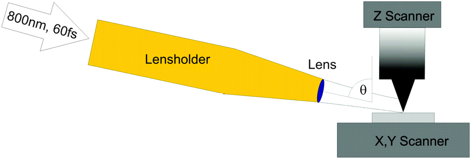 | ||
| Fig. 2 Apertureless scanning near-field microscope set-up. | ||
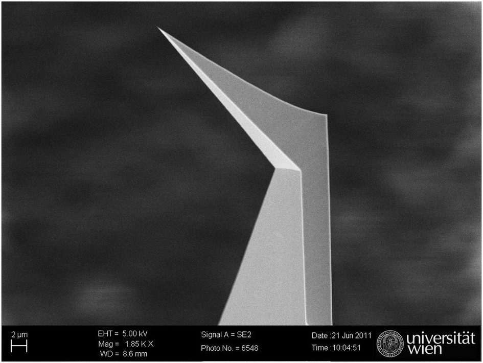 | ||
| Fig. 3 SEM image of the aSNOM tip (ATEC-NC). The special design allows observation of the tip end from the top. This allows accurate pre-alignment of the laser spot on the tip. | ||
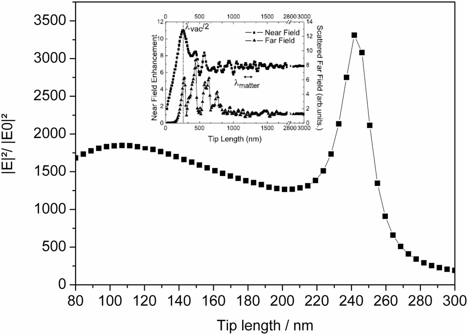 | ||
| Fig. 4 Calculated field enhancement versus tip length for a silicon tip with a radius of 10 nm and an excitation wavelength of 800 nm. A resonance peak appears at approximately 240 nm tip length. Similar behaviour was described before (inset;37 ©IOP Publishing 2013. Reproduced by permission of IOP Publishing. All rights reserved. DOI:10.1088/0957-4484/17/2/022). | ||
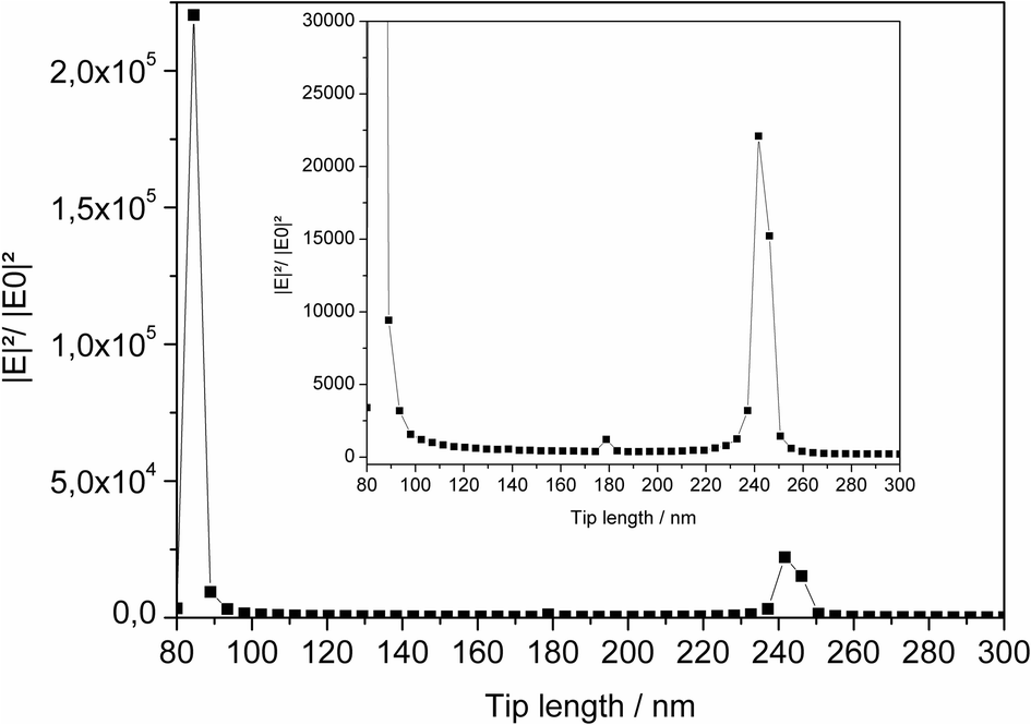 | ||
| Fig. 5 Field enhancement versus tip length for a gold tip with a radius of 65 nm and an excitation wavelength of 800 nm. In the inset the y-axis is magnified to visualize the off-resonance enhancement. The incident laser excites the tip from the left side with an angle of 76°. | ||
3. Results and discussion
3.1 Geometrical investigation
Besides the diameter and the opening angle, especially the tip length has a major influence on the enhancement results. In this context, simulations of short tips (<1000 nm) have to be analyzed carefully because resonance effects may occur leading to an overestimation of the enhancement effects.37,38The field intensity over various tip lengths at an excitation wavelength of 800 nm has been calculated in order to avoid resonance effects. The field enhancement versus tip length is depicted for Si tips (Fig. 4) and Au tips (Fig. 5). The tip length was varied between 80 nm and 300 nm. A length of 300 nm was close to the maximum computable size for the workstation for the chosen discretisation (18 GB memory). The angle of incidence relative to the tip was 76°. The discretisation of the tip was always adapted to the new tip length to guarantee the same element distribution for every tip size.
The radii of the Si and the Au tips were chosen according to the specifications provided by the manufacturer and set to be 10 nm for Si and 65 nm for the Au tips. The pure Si tip showed moderate dependency on the tip length (Fig. 4). However, a field enhancement peaked at a tip length of approximately 240 nm. Similar behaviour has already been reported and was explained by the antenna effect.37
On a Au tip the length dependent field enhancement behaviour was much more pronounced because surface plasmon resonance came into account. Earlier calculations for longer tips showed that the field enhancement decreases moderately with increasing tip length.38 The same behaviour appears in Fig. 5, except for the resonance peaks at a tip length of 85 and 240 nm. The strong resonance around 85 nm, where excitation of propagating surface plasmon polaritons is not expected can be explained by excitation of localized surface plasmons with a resonance frequency of around 800 nm. The peak at 240 nm could also be found for Si tips and therefore indicates a geometrical resonance like the antenna effect. As the tip length increases, the localized plasmon resonance (LPR) is shifted to longer wavelengths, decreasing the local field enhancement.
In practice, it is difficult to match the geometry that fits the resonance conditions for the available laser wavelength. Therefore, this work concentrated on the off-resonance behaviour.
The distribution of the field intensity for a Si tip and an Au tip located 2 nm over an Au surface is shown in Fig. 6. The laser illumination parameters were the same as for the tip length calculations. The modelled tip length was now set to be 300 nm to guarantee off-resonance excitation for Si and Au. The field enhancement for the Si tip was calculated to be 150. This value could be even increased for higher excitation angles because the field enhancement is prohibited by the reflected wave from the surface underneath for small angles of incidence, when Fresnel reflection coefficients are considered (Fig. 7). The diameter of the silicon tip was 20 nm whereas the field under the silicon tip was even more confined enabling a resolution below 10 nm.
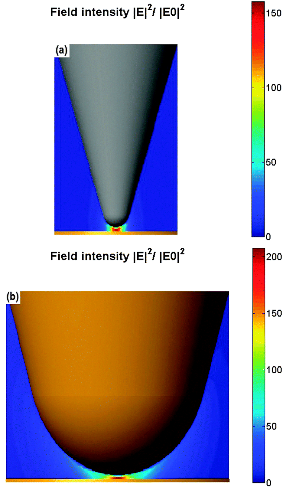 | ||
| Fig. 6 Field enhancement in the tip sample gap of (a) a silicon tip (r = 10 nm) and (b) a gold tip (r = 65 nm) at a distance of 2 nm away from the gold surface. The incident laser excites the tip from the left at an angle of 76°. In the calculation the electric field vector is taken to be parallel to the major axis of the tip. | ||
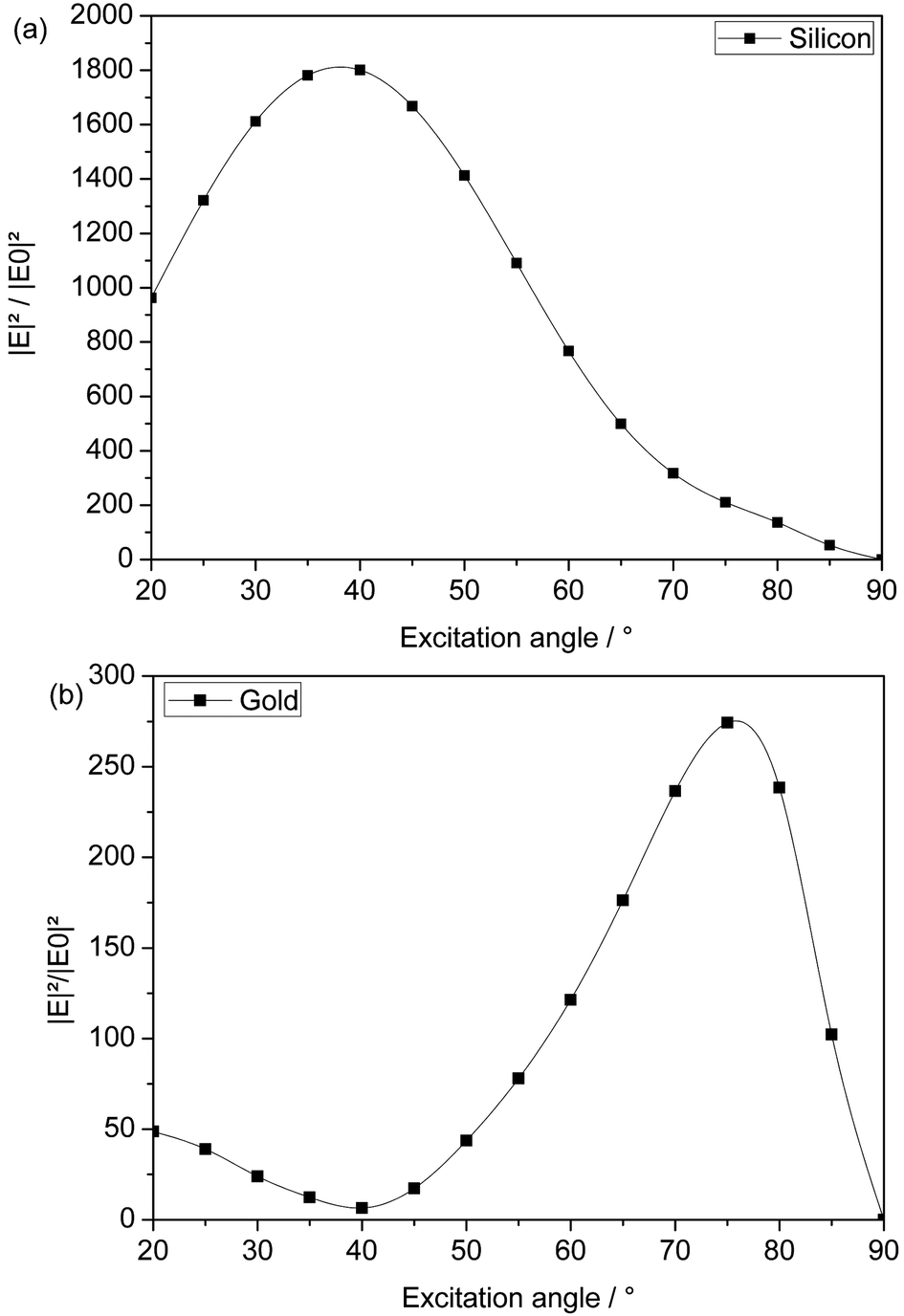 | ||
| Fig. 7 Angle of incidence vs. field enhancement for (a) a silicon tip (r = 10 nm) and (b) a gold tip (r = 65 nm). No enhancement is visible for 90°, which is explained by the phase shift of the reflected wave. | ||
Although the investigations were done under off-resonance conditions the field enhancement for the blunt Au tip was still higher for the selected geometry than for the sharp Si tip. This finding is surprising with respect to the traditional concept in the literature that the field enhancement decreases with increasing radius, because the field confinement also decreases.6,39
It has to be noted that this behaviour is only valid for high excitation angles. Calculations for the field enhancement depending on the excitation angle revealed that the maximum of the field enhancement decreases with greater tip radii but the optimum excitation angle, leading to highest enhancement, shifts to higher angles with respect to the major tip axis (Fig. 7).
The central role of the angle of incidence for a tip without a substrate has already been reported and is attributed to the importance of the electric field vector aligned along the major tip axis.28 When a substrate near the tip is considered, the dependency of the field enhancement on the angle of incidence changes significantly. This can be explained by the fact that the incoming wave will be reflected at the surface underneath the tip. A phase shift comes into play and the destructive interference of the electromagnetic fields leads to a low field enhancement. For accurate evaluations the distance between the tip and the surface has to be taken into account, as well.22,25 Besides the interference of the incoming and reflected wave, multipole excitation also influences the characteristics of the field enhancement dependency on the angle of incidence.40
The calculated field enhancement plotted versus the angle of incidence for a silicon tip with a radius of 10 nm is depicted in Fig. 7a. The calculated range was limited by the opening angle of the investigated tip and corresponds to a tip illumination parallel to its surface. For the chosen geometry, the highest intensity at Si was reached at an angle of incidence of around 40°, which fits previous calculations.37
The calculation for an Au tip with a radius of 10 nm is very similar to the behaviour of the Si tip (not shown here). If the radius is increased to 65 nm, which is more typical for commercial Au-coated Si tips, however, the behaviour changes significantly (Fig. 7b). In this case the maximum enhancement decreases, which has been explained6,39 by the lower confinement of the electric field, as already discussed above, and the angle of maximum field enhancement shifts to higher values.
3.2 Polarization dependency
A strong component of the electric field vector parallel to the major tip axis is important to guarantee high field enhancement, although it has been shown above that the angle of incidence and the vicinity of a surface influence this characteristic decisively. The dependency of the field enhancement on the polarization direction of the incoming laser light exhibits a typical cosine function.41,42 The highest enhancement can be observed for a strong electric field component parallel to the major tip axis.Typical commercial SPM setups, as bedrock for an apertureless scanning near-field microscope, work on the light lever principle, where a sharp tip is situated at the end of a cantilever, whose motion is used for extracting various information of the surface. It is obvious that the illumination of the sharp tip also causes heating of the entire cantilever system and therefore changes its mechanical properties. These changes can be utilized to determine the temperature of the tip. For oscillating cantilevers the shift in the resonance frequency is chosen as a reasonable tool for easily estimating the temperature of the tip.43 As the resonance frequency shift is caused by the overall heating of the tip–cantilever system, a complementary tool is necessary to calibrate the resonance frequency shift with the temperature of the tip. For this, Raman spectroscopy is favoured because silicon tips provide a Raman mode which is highly temperature dependent.44
The combination of these two techniques was realized by an SPM located on an inverted microscope. A resonance frequency shift of approximately 1 Hz for 1 K tip temperature rise was observed.43 Calculated tip temperatures as a function of the polarization angle and the temperature have shown a similar cosine characteristic to typical theoretical field enhancement plots as a function of the polarization angle.42
This theoretical investigation was confirmed experimentally in this work, using the resonance frequency shift as observable for the tip heating controlled by Raman measurements. The resonance frequency shift for different polarization angles was determined in the present investigation (Fig. 8a). The determination of the resonance frequency is only possible without a surface nearby because this would prohibit accurate measurements. The characteristic of the curve fits perfectly the theoretical prediction, except for the extreme values, where the cosine curve profile is distorted.
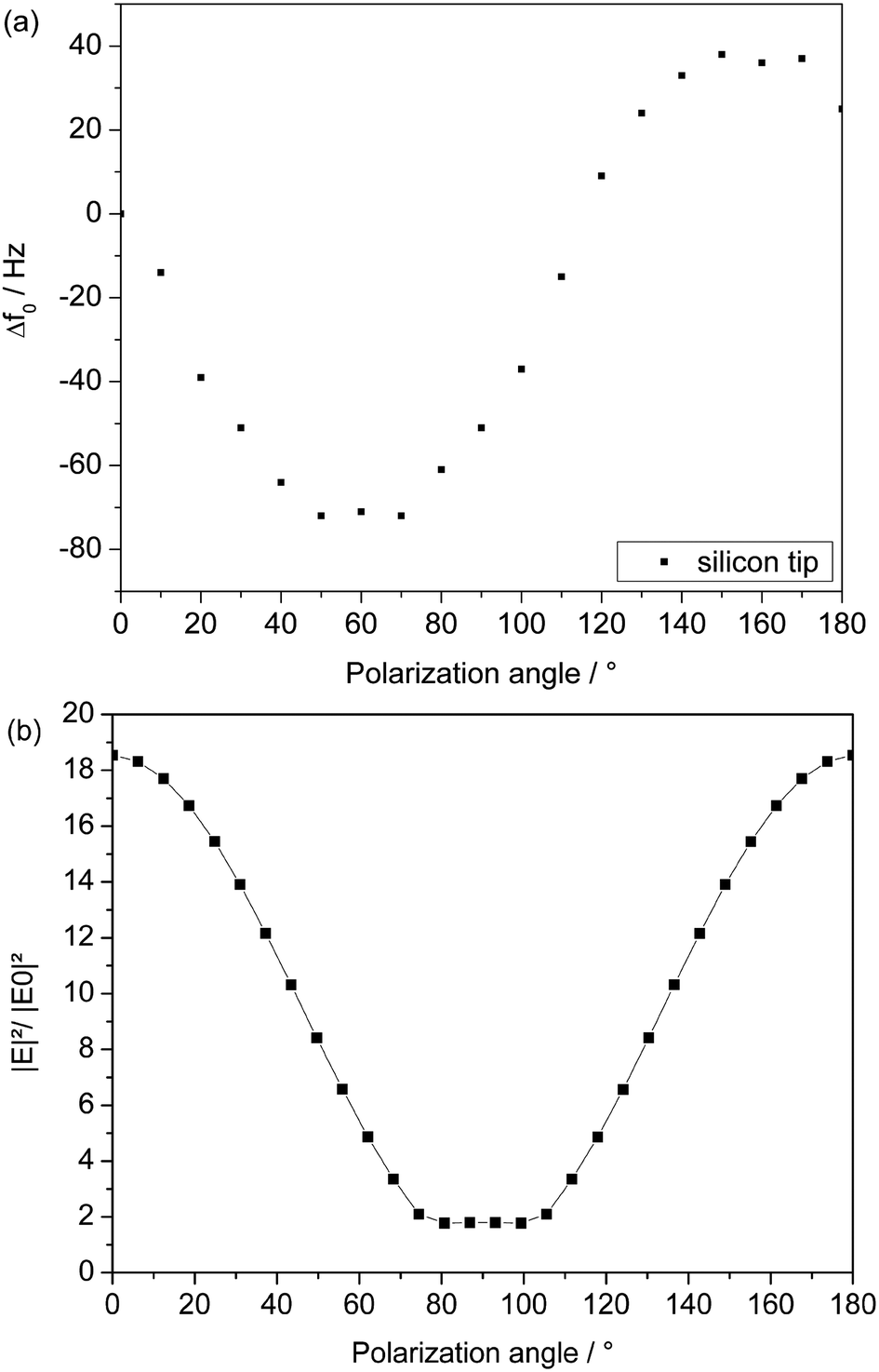 | ||
| Fig. 8 (a) Measured frequency change due to the heating of the cantilever for a silicon tip. The lack of the reflected wave influences the charge distribution at the tip and leads to a distortion of the ideal behaviour, marked by two ellipses. The y-axis is inverted for better comparison. High negative frequency shift means low tip temperature in this case. (b) Simulated field enhancement dependency on the polarization angle for a silicon tip. Parameters are according to the experiment. The curve characteristic is explained by the fact that the maximum field intensity is not taken from the very end of the tip but from the whole structure, which is more reasonable when the overall heating of the tip–cantilever system is measured. | ||
To understand this behaviour in more detail, further simulations have been performed, where the model parameters were adapted to the experimental setup. It turned out that, due to the lack of a substrate underneath the tip, no reflected waves emerge. Therefore the distribution of the surface charges is slightly shifted leading to a distortion of the field enhancement factor in the profile of the curve, especially when the maximum enhancement value is not taken from the very end of the tip (Fig. 8b). Different appearance of the curve profile between theory and experiment is explained by discrepancies in the shape of the ideal structure (simulated) and the real structure (measured).
The same investigation was performed for Au tips. Au tips are made out of a silicon core coated with an Au layer resulting in a much greater tip radius. Therefore the plateau of low field enhancement broadens, which is obvious for s-polarized light (Fig. 9). The fine structure of the curve for s-polarization can be explained by multipole excitation.
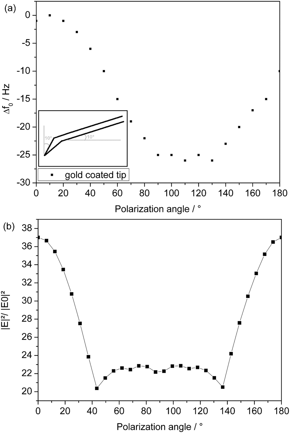 | ||
| Fig. 9 (a) Measured frequency shift of a gold coated silicon tip. The shift of the maximum enhancement is caused by the inherent vertical tilt of the cantilever due to the mounting (inset). The drift in the absolute frequency values is the overall heating effect of the whole system. The y-axis is inverted for better comparison. (b) Simulated polarization dependency for a gold tip. Parameters are according to the experiment. | ||
The absolute frequency shift of the Au coated cantilever was less pronounced than for the Si cantilever in the experiment (Fig. 8a and 9a). This reveals the higher reflectivity of Au for 800 nm laser radiation compared to Si and the homogeneous Au coating which minimizes the bimetallic influence in contrast to the Si cantilever, where only the upper surface of the cantilever is coated.
The different position of the maximum values for Si and Au experiments with respect to the simulated results is due to the experimental circumstances (Fig. 2). As the illumination was directed from the side, the vertical tilt of the tip due to the mounting position of the cantilever on the scanner has to be taken into account. In addition, the orientation of the tip relative to the cantilever is also different for the Si and the Au tip.
3.3 Influence of the coating thickness
Au tips described in the simulations above and reported in the literature have always been regarded as solid tips. This may be true for STM or shear force measurements. For SPM measurements there are no solid gold tips available and thus Si tips with various Au coating thicknesses have to be used. The range extends from 5 to 65 nm Au coating thickness depending on the manufacturer.In order to investigate the influence of the different coating thicknesses, a new model has been established where the overall radius defined by the outer Au coating shell was kept constant and the thickness of the metal coating was adjusted by reducing the size of the Si core in order to avoid the influence of geometric changes (Fig. 10).
 | ||
| Fig. 10 Model to simulate the influence of different gold coating thicknesses. The overall radius is kept constant and the size of the inner silicon core is varied to change the thickness of the gold coating which is determined by the outer shell. In this case the thickness of the gold coating is 25 nm. | ||
Spectra for excitation wavelengths from 300–900 nm were calculated for each coating thickness. The radius of the outer shell was 75 nm. The thickness of the coating was varied within the range known as typical commercial coating thickness (5–65 nm). These calculations were performed at the Vienna Scientific Cluster (VSC-1) because the double tip structure increased the element number tremendously. The spectra of pure Si and pure Au tips (Fig. 11a) were compared with the spectra of various gold coating thicknesses (Fig. 11b). The differences in the coating thickness influenced the spectra excessively until a thickness of ≥40 nm was reached. This value corresponds to the calculated skin depth for wavelengths between 300–900 nm, where most of the spectrum is already absorbed at around 40 nm (Fig. 12b). For thicknesses above 40 nm, the coated tip behaves like a solid Au tip, only the absolute field enhancement values change. In Fig. 11b, three exemplary gold coating thicknesses are illustrated. The intensity is normalized for better visualization.
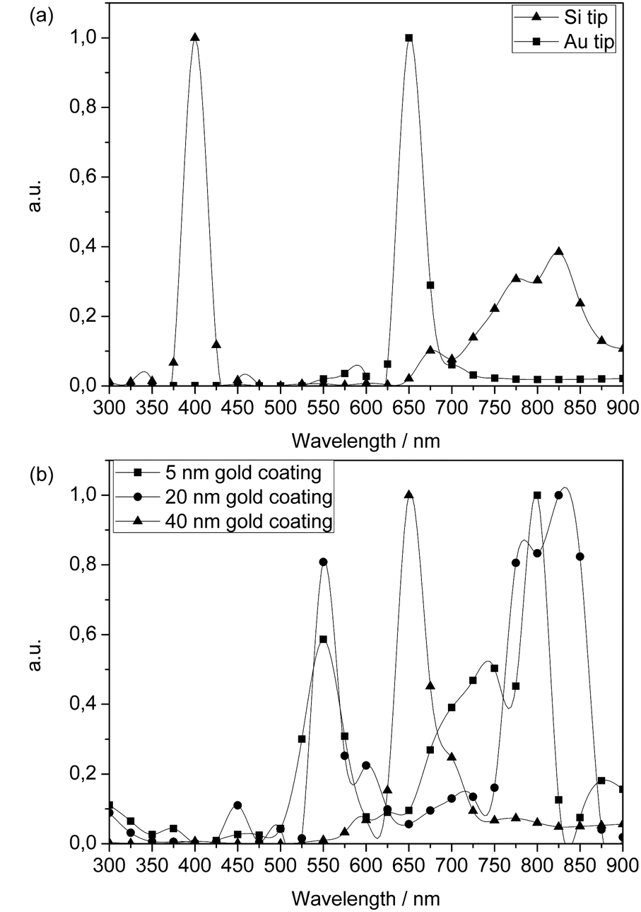 | ||
| Fig. 11 Field enhancement study at different wavelengths for different gold coatings. (a) Wavelength dependency for solid silicon and solid gold tips. (b) Coating thickness dependency. No significant change in the spectra for gold coatings thicker than 40 nm can be observed and the resonance peak at 650 nm is clearly visible. The calculated points were connected by a spline function as guide for the eye. | ||
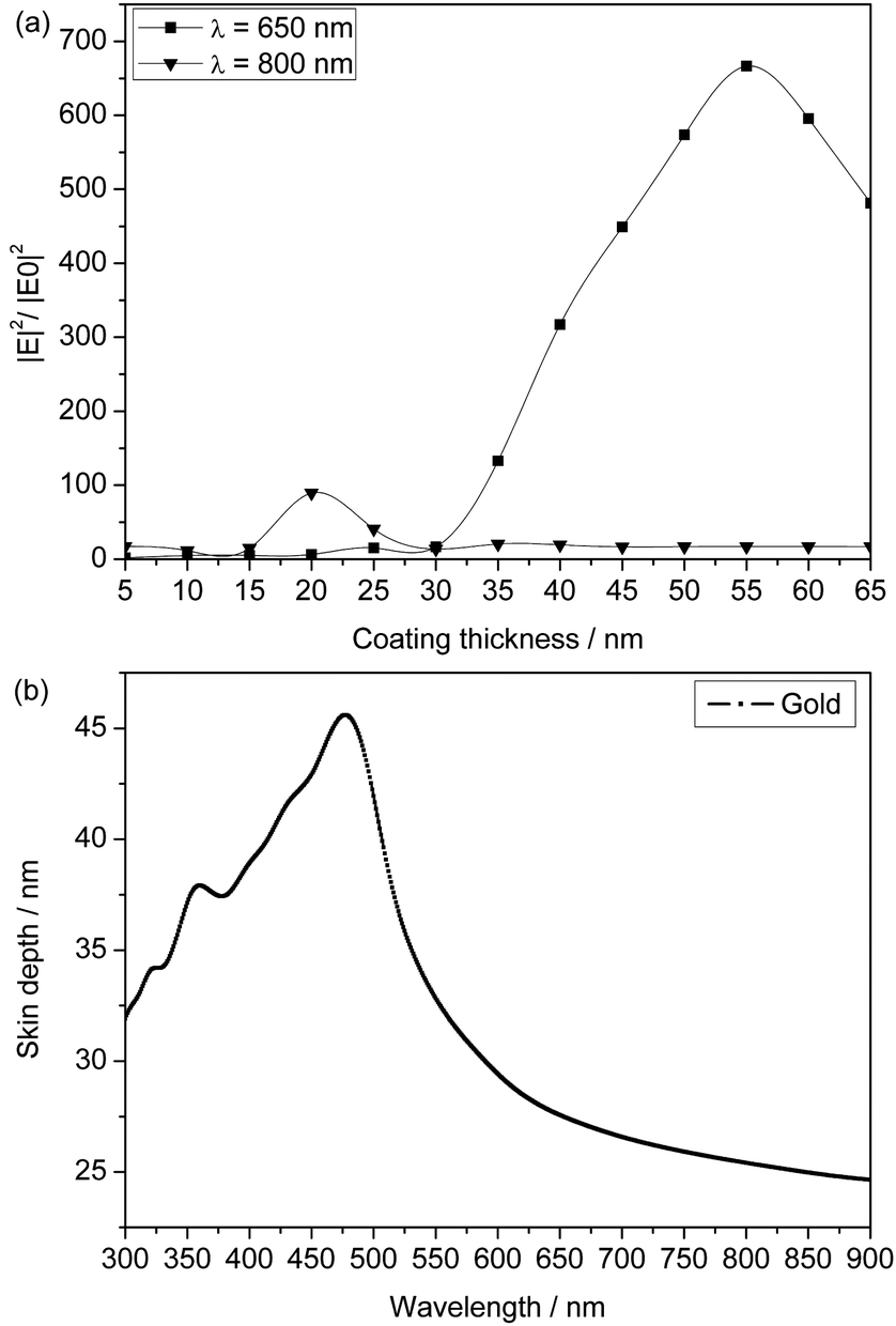 | ||
| Fig. 12 (a) Maximum field enhancement for 650 and 800 nm excitation wavelength for different coating thicknesses. The maximum field enhancement for the resonance case is twice the skin depth. (b) Skin depth for gold at various wavelengths calculated according to M. I. Stockman.45 | ||
The highest field enhancement is achieved for an excitation wavelength of 650 nm, which corresponds to the resonance case for the investigated parameters and a coating thickness of 55 nm (Fig. 12a), which is exactly two times the skin depth in Au for this wavelength.
A coating thickness of 20 nm would yield a maximum enhancement at 800 nm laser radiation, used in the experimental part. At 650 nm excitation wavelength, however, the maximum value would be nearly seven times greater.
4. Conclusions
Theoretical investigations have concentrated on the influence of geometrical and illumination parameters on the field enhancement between a pointed SPM tip and a substrate. The simulations have been performed with the MNPBEM toolbox33 for Matlab, which is based on the Boundary Element Method (BEM).Field enhancement was calculated for different tip lengths. At Au tips the resonance behaviour was much more pronounced than at Si tips because of the stronger surface plasmon resonance. In practice it is difficult to find the exact geometry, which fits the resonance conditions for an available laser wavelength. Therefore the off-resonance behaviour was investigated, yielding moderate enhancement factors.
The influence of the angle of incidence for different tip geometries was also evaluated. It was shown that a shift to higher angles of incidence for the maximum enhancement can be observed for greater tip radii.
A new method to optimize the alignment of the electric field vector along the major tip axis, by measuring the resonance frequency, was developed and demonstrated. This can be crucial for side illuminating SPM setups to reach maximum field enhancement.
The influence of the coating thickness was investigated for the first time. Simulations were performed with a constant geometry. Coating thicknesses below 40 nm showed a drastic influence both on the resonance wavelength and the enhancement. This indicates that precise control of the thickness is mandatory to enable reproducible experimental conditions.
To exploit the full potential of field enhancement in apertureless Scanning Near-field Microscopy, the use of an optical parametric amplifier (OPA) to scan over a broad range of wavelengths and measure the tip response simultaneously appears to be a very promising approach.
Acknowledgements
The authors acknowledge financial support from the Österreichische Forschungsgemeinschaft (ÖFG), the University of Vienna (KWA Programm), the Austrian Science Fund FWF under Project No. P24511-N26, and the SFB NextLite. We are grateful to Alexander Milner for his support with the measurements, Euclides Almeida (both Weizmann Institute of Science) for critical reading of the manuscript, and Thomas Huber (Vienna University of Technology) for indispensable assistance in the numerical calculations at the Vienna Scientific Cluster (VSC), Austria.Notes and references
- A. Hartschuh, Angew. Chem., Int. Ed., 2008, 47, 8178–8191 CrossRef CAS PubMed.
- R. Hillenbrand and F. Keilmann, Appl. Phys. Lett., 2002, 80, 25–27 CrossRef CAS.
- Y. Inouye and S. Kawata, Opt. Lett., 1994, 19, 159–161 CrossRef CAS.
- J. Koglin, U. C. Fischer and H. Fuchs, Phys. Rev. B: Condens. Matter Mater. Phys., 1997, 55, 7977–7984 CrossRef CAS.
- A. Zayats and D. Richards, Nano-Optics and Near-Field Optical Microscopy, Artech House, Boston/London, 2009 Search PubMed.
- M. B. Raschke and C. Lienau, Appl. Phys. Lett., 2003, 83, 5089–5091 CrossRef CAS.
- L. Novotny and S. J. Stranick, Annu. Rev. Phys. Chem., 2006, 57, 303–331 CrossRef CAS PubMed.
- J. M. Gerton, L. A. Wade, G. A. Lessard, Z. Ma and S. R. Quake, Phys. Rev. Lett., 2004, 93, 180801 CrossRef.
- M. S. Anderson, Appl. Phys. Lett., 2000, 76, 3130–3132 CrossRef CAS.
- N. Hayazawa, Y. Inouye, Z. Sekkat and S. Kawata, Opt. Commun., 2000, 183, 333–336 CrossRef CAS.
- A. Hartschuh, N. Anderson and L. Novotny, J. Microsc., 2003, 210, 234–240 CrossRef CAS.
- B. Pettinger, B. Ren, G. Picardi, R. Schuster and G. Ertl, Phys. Rev. Lett., 2004, 92, 096101–096101 CrossRef.
- C. C. Neacsu, J. Dreyer, N. Behr and M. B. Raschke, Phys. Rev. B: Condens. Matter Mater. Phys., 2006, 73, 193406 CrossRef.
- E. Bailo and V. Deckert, Chem. Soc. Rev., 2008, 37, 921–930 RSC.
- B.-S. Yeo, J. Stadler, T. Schmid, R. Zenobi and W. Zhang, Chem. Phys. Lett., 2009, 472, 1–13 CrossRef CAS PubMed.
- A. L. Demming, F. Festy and D. Richards, J. Chem. Phys., 2005, 122, 1–7 CrossRef PubMed.
- B. Pettinger, B. Ren, G. Picardi, R. Schuster and G. Ertl, J. Raman Spectrosc., 2005, 36, 541–550 CrossRef CAS.
- B. Ren, G. Picardi and B. Pettinger, Rev. Sci. Instrum., 2004, 75, 837–841 CrossRef CAS.
- S. Kawata and V. M. Schalaev, Tip enhancement, Elsevier, Amsterdam, 2007 Search PubMed.
- A. Chimmalgi, C. P. Grigoropoulos and K. Komvopoulos, J. Appl. Phys., 2005, 97, 1–12 CrossRef.
- J. T. Krug, E. J. Sanchez and X. S. Xie, J. Chem. Phys., 2002, 116, 10895–10901 CrossRef CAS.
- Z. B. Wang, B. S. Luk'Yanchuk, L. Li, P. L. Crouse, Z. Liu, G. Dearden and K. G. Watkins, Appl. Phys. A: Mater. Sci. Process., 2007, 89, 363–368 CrossRef CAS.
- P. R. Sajanlal, C. Subramaniam, P. Sasanpour, B. Rashidian and T. Pradeep, J. Mater. Chem., 2010, 20, 2108–2113 RSC.
- Y. F. Lu, Z. H. Mai and W. K. Chim, Jpn. J. Appl. Phys., Part 1, 1999, 38, 5910–5915 CrossRef CAS.
- O. J. F. Martin and C. Girard, Appl. Phys. Lett., 1997, 70, 705–707 CrossRef.
- O. J. F. Martin, C. Girard and A. Dereux, Phys. Rev. Lett., 1995, 74, 526–529 CrossRef CAS.
- J. Jersch and K. Dickmann, Appl. Phys. Lett., 1996, 68, 868–870 CrossRef CAS.
- L. Novotny, R. X. Bian and X. Sunney Xie, Phys. Rev. Lett., 1997, 79, 645–648 CrossRef CAS.
- O. J. F. Martin and M. Paulus, J. Microsc., 2002, 205, 147–152 CrossRef CAS.
- A. Downes, D. Salter and A. Elfick, J. Phys. Chem. B, 2006, 110, 6692–6698 CrossRef CAS PubMed.
- P. I. Geshev, U. Fischer and H. Fuchs, Phys. Rev. B: Condens. Matter Mater. Phys., 2010, 81 Search PubMed.
- F. Demming, J. Jersch, K. Dickmann and P. I. Geshev, Appl. Phys. B: Lasers Opt., 1998, 66, 593–598 CrossRef CAS.
- U. Hohenester and A. Trügler, Comput. Phys. Commun., 2012, 183, 370–381 CrossRef CAS PubMed.
- F. J. García de Abajo and A. Howie, Phys. Rev. B: Condens. Matter Mater. Phys., 2002, 65, 1154181 CrossRef.
- L. Novotny and B. Hecht, Principle of Nano-Optics, Cambridge University Press, New York, 2006 Search PubMed.
- P. B. Johnson and R. W. Christy, Phys. Rev. B, 1972, 6, 4370–4379 CrossRef CAS.
- R. Esteban, R. Vogelgesang and K. Kern, Nanotechnology, 2006, 17, 475–482 CrossRef CAS.
- W. Zhang, C. Xudong and O. J. F. Martin, J. Raman Spectrosc., 2009, 40, 1338–1342 CrossRef CAS.
- N. Behr and M. B. Raschke, J. Phys. Chem. C, 2008, 112, 3766–3773 CAS.
- W. X. Sun and Z. X. Shen, J. Opt. Soc. Am., 2003, 20, 2254–2259 CrossRef.
- L. Aigouy, A. Lahrech, S. Grésillon, H. Cory, A. C. Boccara and J. C. Rivoal, Opt. Lett., 1999, 24, 187–189 CrossRef CAS.
- X. Chen and X. Wang, Nanotechnology, 2011, 22 Search PubMed.
- A. A. Milner, K. Zhang, V. Garmider and Y. Prior, Appl. Phys. A: Mater. Sci. Process., 2010, 99, 1–8 CrossRef CAS.
- M. Balkanski, R. F. Wallis and E. Haro, Phys. Rev. B: Condens. Matter Mater. Phys., 1983, 28, 1928–1934 CrossRef CAS.
- M. I. Stockman, Opt. Express, 2011, 19, 22029–22106 CrossRef PubMed.
| This journal is © the Owner Societies 2014 |