
 Open Access Article
 This Open Access Article is licensed under a
 Creative Commons Attribution 3.0 Unported Licence
Structural transformation of lattice defects in free-spreading growth of bulk SiC crystals
T. S.
Argunova
a,
M. Yu.
Gutkin
bcd,
J. H.
Je
 *e,
J. H.
Lim
f,
E. N.
Mokhov
a and
A. D.
Roenkov
a
*e,
J. H.
Lim
f,
E. N.
Mokhov
a and
A. D.
Roenkov
a
aIoffe Physical-Technical Institute, RAS, St. Petersburg, Russia
bInstitute of Problems in Mechanical Engineering, RAS, St. Petersburg, Russia
cDepartment of Mechanics and Control Processes, Polytechnical University, St. Petersburg, Russia
dUniversity of Information Technologies, Mechanics and Optics, St. Petersburg, Russia
eX-ray Imaging Center, Department of Materials Science and Engineering, Pohang University of Science and Technology, Pohang, Republic of Korea. E-mail: jhje@postech.ac.kr; Fax: +82 054 2792992; Tel: +82 054 2792143
fBeamline Division, Pohang Accelerator Laboratory, Pohang, Republic of Korea
First published on 15th August 2014
Abstract
Using synchrotron X-ray topography and phase-contrast imaging, we investigated lattice defects in bulk SiC crystals grown by physical vapor transport in a free spreading condition. We find that polytype inclusions appearing at initial growth stage are overgrown by the matrix, making pores which are then transformed into micropipes with a low density of 10 cm−2, in particular, in the lateral region. We propose that complex planar defects configured from dislocations and micropipes are transformed into slit pores via vacancy-diffusion and micropipes-attraction mechanisms. Our finding suggests that suppression of the nucleation of foreign polytype inclusions is a key approach for providing high quality free spreading SiC growth.
1. Introduction
SiC power devices capable of handling large currents require a large device area of a few millimeters. However, the mass production of large size SiC single crystals without lattice defects, such as threading dislocations1,2 and dislocated micropipes,3,4 still remains a problem. It has been pointed out that if the growing crystal spreads well beyond the seed contour during physical vapor transport growth, such defects can be drastically reduced by preventing seed defects from propagating outside the basal plane facet.5–8 Indeed, 6H- and 4H-SiC crystals5,6 up to 35 mm in diameter and 20 mm in height6 were produced with significant density reduction in threading dislocations and micropipes in the lateral crystal part compared to those of the seed.6,9,10 However, the other defects nonspecific in conventional SiC growth, such as stacking faults,10 pores and agglomerations of micropipes,9 were commonly present.The interesting feature of free-spreading crystals is a well pronounced hexagonal habit [Fig. 1(a)]. Unlike single-faceted boules grown along the basal plane normal [0001], they exhibit prismatic and rhombohedral facets in addition to the basal plane one.6,9,10 So “faceted crystals” is another name for free-spreading ones. Owing to their faceted structure, free-spreading crystals are served as prismatic11 or rhombohedral12,13 plane seeds. For example, a repeatable growth process on the prismatic planes, or “a-faces”, was proven especially effective in reducing dislocations and micropipes.14 Meanwhile, the growth on the nonstandard surfaces requires large seed crystals of low defect density.
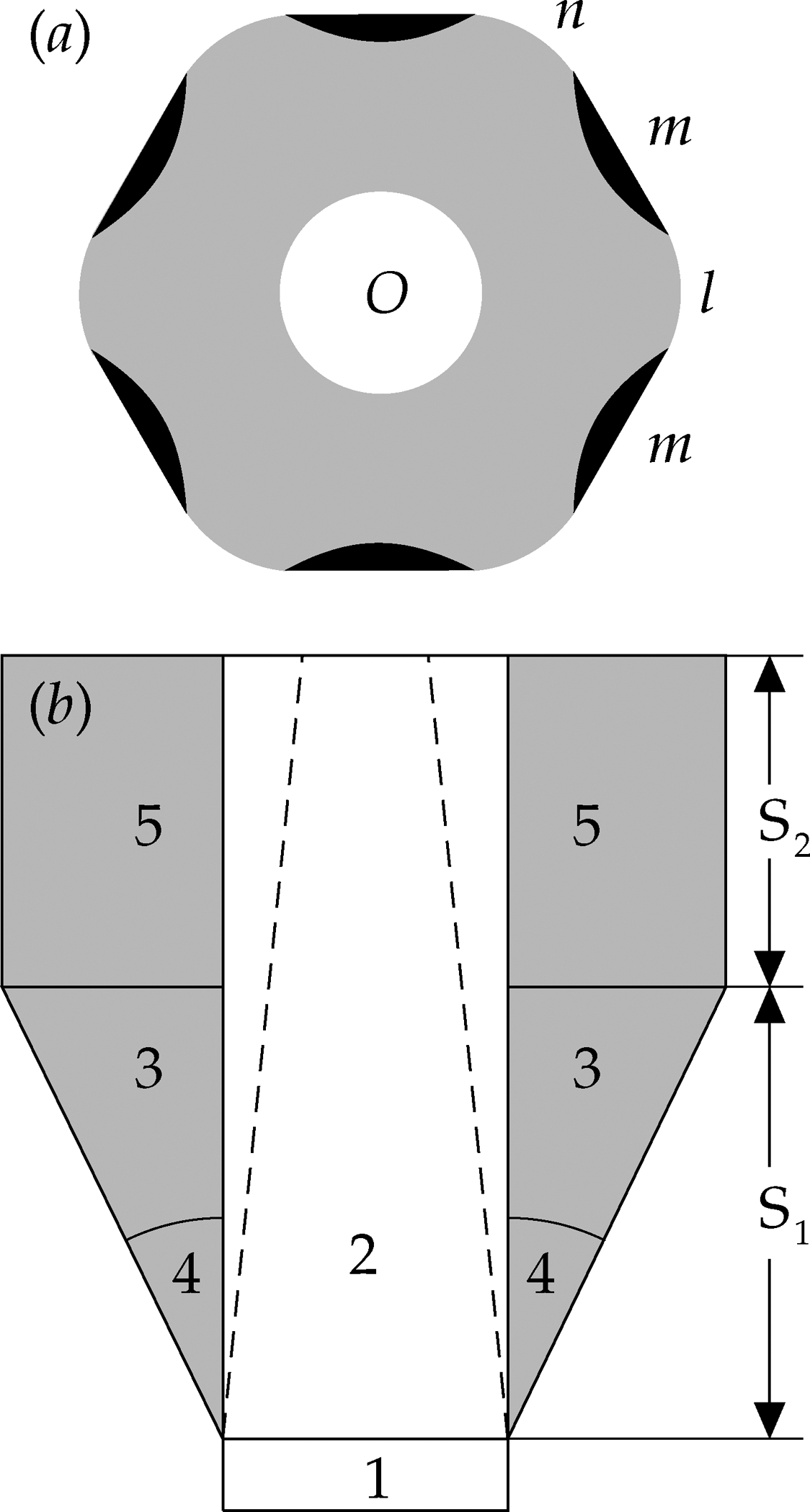 | ||
| Fig. 1 (a) Schematic diagram of a faceted SiC boule (top view) displaying the core region (white) and the lateral region (grey). O is the basal plane facet, m is the hexagonal prism facet, n and l are the nonsingular facets of right and left trigonal prisms, respectively. (b) Sketch of the boule (side view) illustrating the first S1 and the second S2 growth stages; 1 is the seed, 2 is the core region, 3 is the material laterally grown during S1, 4 is the lateral growth angle, 5 is the material axially grown during S2. Dashed lines show the reduction of the core size during S2. | ||
For conventional SiC growth, many aspects of propagation, interaction and conversion of lattice defects were successfully explained. Specifically, basal-plane, elementary screw, threading edge dislocations2 and micropipes3 were examined in detail. It is known that one of the primary reasons for the appearance of dislocations and micropipes in bulk SiC crystals are due to foreign polytype inclusions.15–19 Threading dislocations are generated due to elastic stresses at the boundaries of polytype inclusions15,17,19 and dislocated micropipes are generated by coalescing elementary screw dislocations.16,17 For free spreading SiC growth, however, detailed understanding of defects still remains unclear. Our study is aimed at elucidating the transformation of newly generated (rather than seed-provoked) defects during free-spreading growth. Using synchrotron radiation (SR) topography combined with phase contrast imaging,20 we show that dislocations and micropipes introduced by foreign polytype inclusions cause the formation of complex planar defects which can be transformed into slit pores.
2. Samples and techniques
2.1. Crystal growth
The SiC crystal growth by a sublimation sandwich method6 was divided into two stages. In the first stage, S1 in Fig. 1(b), the crystal was grown in the [0001] axial direction (i.e., normal to the surface of the seed (1)) while simultaneously expanding laterally. After the crystal had expanded to the desired diameter, lateral growth was suppressed while axial growth was enhanced during the second stage of the growth, S2. The grown crystal was thus comprised of the core region (2), the laterally grown area (3) and the axially grown material (5).Generally the lateral growth angle (4) must be greater than 25°, preferably greater than 45°. The growth conditions were chosen to reduce the size of the core region during growth, as illustrated in Fig. 1(b). The lateral expansion is limited by the crucible size, which is determined by the ability to achieve the required temperature gradients.
As a seed, we used a (0001) 6H-SiC crystalline plate ~8 mm in diameter (laterally spread to a boule of 20–30 mm in diameter). The original property of the seed crystal is a high crystalline quality that minimizes the propagation of defects within the core region. Preferably the seed crystal was defect free. In our experiments the dislocation density in a seed was ~104 cm−2 and the micropipe density was ~10 cm−2.
The growth was carried out at 2000–2300 °C in a tantalum crucible. The Ar partial pressure was controlled between 10−1 to 10−4 Torr. The growth rate was 0.1 to 1.5 mm per hour. The temperature profile inside the crucible was controlled to allow the growing crystal to freely spread sideways beyond a seed. The temperature gradient in the growing crystal was maintained less than 5 °C cm−1.
Several wafers cut perpendicular to the [0001] growth direction were obtained from the 6H-SiC boules. They were mechanically and chemically mirror-polished on both sides to remove a damage layer and surface roughness.
2.2. X-Ray imaging
X-Ray imaging experiments were performed at 6D X-ray micro-imaging beamline in Pohang Light Source of South Korea, the 3rd generation SR source operating at 3 GeV. The experimental setup is shown in Fig. 2(a). The beam source with a size 160 × 60 μm (H × V) from a bending magnet was located 35 m from the sample. The topography and phase contrast setups were arranged in a sequence. After passing through a slit system (S) in front of the hutch, polychromatic radiation arrives at the sample mounted on a holder (O1) with three translational axes (0.1 μm accuracy), tilting and rotation. Behind the sample, the radiation is converted into visible light by a CdWO4 crystal-scintillator (150–200 μm thick). The sample-scintillator distance O1C can be varied from 5 mm to 1.5 m. The visible light is reflected from a polished silicon mirror (M) and reaches CCD camera (D1). The light image was magnified by a lens (L). The CCD matrix had 4008 (H) × 2672 (V) pixels size, one pixel being 9 μm (H) × 9 μm (V). By a 20× lens the effective resolution was 0.45 μm, and the view field was 1804 × 1202 μm2. | ||
Fig. 2 (a) Scheme illustrating in-line phase-contrast imaging (dashed line) and topography experiments; here S is the slit, O1 and O2 are the sample positions, C is the crystal-scintillator, M is the silicon mirror, L is the magnifying lens, D1 and D2 are the CCD detectors, B is the beam-stop, and F is the film. (b) Laue topographs taken simultaneously from the (0001) wafer of 6H-SiC. The [![[1 with combining macron]](https://www.rsc.org/images/entities/char_0031_0304.gif) 120] direction is vertical and the [0001] direction is 3° off the beam. The sample-to-film distance is 145 mm. 120] direction is vertical and the [0001] direction is 3° off the beam. The sample-to-film distance is 145 mm. | ||
The phase-contrast microscope can be moved up to allow the beam to come to the other sample holder (O2) where a topography experiment can be carried out. The detector for topography (D2) was the Naomi multi-CCD sensor of a large area. By opening the slits (S), a wide beam is provided at the SiC sample on the holder (O2) with rotational, tilting or translational stages. Laue topographs were recorded using a high-resolution film KODAK SR-45 (F). Fig. 2(b) shows an example of the film with many reflections recorded at once. The reflections form a pattern characteristic of the symmetry of the crystal structure and the orientation of the crystal with respect to the beam. Each ‘spot’ was further enlarged with an optical microscope to obtain a high resolution topograph.
The Laue patterns were indexed using standard 6H-SiC crystal structure data. In the case of the Laue pattern in Fig. 2(b), experimental and calculated reflections overlay when the sample, fixed perpendicular to the beam at the beginning, was rotated by 3° about the [120] vertical direction, thereby verifying that the sample wafer is a (0001) 6H-SiC single crystal.
3. Results
A photograph of the 6H-SiC wafer is shown in Fig. 3. The axial wafer region is marked with a circle while the lateral one with a periodic array of dice. The block-like contrasts in the axial region are due to foreign polytype inclusions21 generated close to the seed, as revealed by photoluminescence (data not shown). The perimeter of the lateral region consists of arc and straight edges that correspond to singular {100} facets of the hexagonal prism m and (![[2 with combining macron]](https://www.rsc.org/images/entities/char_0032_0304.gif) 110), (110), (110) (or (20), (20), (20)) nonsingular facets of right n (or left l) trigonal prisms, respectively. A few elongated features extending in [20] and [110] directions of the lateral region are pores which will be discussed later.
110), (110), (110) (or (20), (20), (20)) nonsingular facets of right n (or left l) trigonal prisms, respectively. A few elongated features extending in [20] and [110] directions of the lateral region are pores which will be discussed later.
 | ||
| Fig. 3 Photograph of a wafer cut off perpendicular to the [0001] growth direction. The lateral part is covered with a periodic array of dice. The prismatic faces {100} are delineated by straight sections while the {20} facets are drawn out by corners. The dices highlighted by white squares and marked from A to F are displayed in Fig. 4. | ||
By treating the wafer in molten KOH, we were able to evaluate the density of the etch pits formed on its surface. Fig. 4 demonstrates representative X-ray topographs of the etching features in six dices (4 mm2 each) highlighted in the diagram of Fig. 3 by white squares (marked from A to F). One can see that there are no etching features at the periphery of the lateral part (Fig. 4, E and F). But the etch pit density increases when going from the periphery to the middle of the lateral part (Fig. 4, C and D) and toward the boundary of the axial region (Fig. 4, A and B). The average etch pit density is 1.6 × 103 cm−2 with 91% of them close to the periphery of the axial part.
 | ||
| Fig. 4 Some fragments of the Lang topography image showing KOH-etched features (A, B) in an external axial region; (C, D) in a middle lateral region; and (E, F) in an external lateral region. Reflection 10.10, CuKα radiation. | ||
Mokhov et al.6 put forward that under optimal growth conditions no micropipes were generated in the lateral regions of free spreading crystals with a reduced density of dislocation etch pits of 10 cm−2. Under non-optimal conditions, however, parasitic polytypes were generated.6 The high density of the etch pits in our data is therefore attributed to polytype transformation.19
The density of micropipes was measured using a phase contrast imaging technique. Fig. 5(a) and (b) demonstrate phase-contrast images of micropipes recorded in the lateral part of another wafer, prepared from the same 6H-SiC boule. One can see that micropipes run in various directions instead of lying parallel to the c-axis. The contrasts of the micropipes varied along their axes as the wafer was rotated (a, b). Black contrast arises when the angle between the micropipe axis and the beam direction becomes very small,22 owing to irregular shapes of micropipes, as sketched in Fig. 5(c). The micropipe M1M2 that slightly deviates from the beam direction M1B is projected as BM2 onto the exit wafer surface. The projection length BM2 can be significantly changed by rotating the wafer about the axes perpendicular to the beam direction: T1 or T2.
 | ||
| Fig. 5 (a, b) Phase contrast images of micropipes. (c) Schematic diagram showing the SR beam (M1B), the micropipe (M1M2) and the micropipe projection onto the sample surface (M2B). T1 and T2 are the sample rotations about the axes perpendicular to the beam. | ||
On the wafer diagram (Fig. 6) rectangular areas numbered I–IV and marked A, B are the phase contrast maps which relate to m and n facets, respectively. Map I comprised fifteen view fields 2.2 mm2 each, and covered an area of 0.32 cm2. Map I revealed three micropipes. Map II was patched from eleven view fields and revealed 1 micropipe, and so on. The calculation results are summarized in Table 1. Inside the total area of 1.4 cm2 we found 13 micropipes and evaluated the micropipes density as 9.3 cm−2.
 | ||
| Fig. 6 Schematic diagram of a wafer containing phase-contrast maps marked I–IV, A and B which revealed images of the micropipes. The inset (with a scale bar of 150 μm) presents a phase-contrast image of a slit pore marked with a black arrowhead in the diagram. The white arrowhead points to the position in the sample where the topograph (shown in Fig. 7) was taken. The orientation of the sample surface was (0001). The position of the sample with respect to the beam is seen by the {010} and {110} facets. | ||
| Map | Area, cm2 | Micropipes |
|---|---|---|
| I | 0.32 | 3 |
| II | 0.24 | 1 |
| III | 0.22 | 0 |
| IV | 0.19 | 4 |
| A | 0.17 | 3 |
| B | 0.26 | 2 |
Fig. 6 shows linear features extending in the [110], [20], [110], and [20] directions, similar to those in Fig. 3. The phase contrast image in the inset, taken at the place marked with a black arrowhead in Fig. 6, displays slit pore and micropipes. One can see that the micropipes incline towards the pore and tend to be absorbed by it.
Using white radiation topography we revealed misorientation and strain contrasts, as shown in Fig. 7. The position in the sample where the topograph was taken is sketched by a box (with a white arrowhead) in Fig. 6. The dark (1, 2) or bright (3) contrasts of the linear features (1–3) are attributed to sub-grain and grain boundaries (GB). In fact, the neighboring misoriented regions satisfy the Bragg condition for corresponding different wavelengths; as a result the reflected beams have different directions in space and can either overlap or diverge. This makes dark or bright contrast, depending on the relative misorientation of the regions.23
 | ||
| Fig. 7 White radiation topograph of a SiC wafer. The grain boundaries between the misoriented regions are marked as 1, 2 and 3. | ||
4. Discussion
Based on our observations, we can subdivide the observable defects into two categories which are quite different both in their origin and region of appearance. The first category includes threading dislocations and dislocated micropipes. These defects are inherited, in part, from the seed crystal, and develop with the growing crystal in its axial region. At the same time, they can be newly generated during the crystal growth. As reported,15–17,24 we think that one of the primary reasons for the appearance of micropipes in bulk SiC crystals is foreign polytype inclusions.18,19 The crystals under consideration contained such inclusions.The second category of the growth defects includes planar slit pores which were revealed in the lateral regions. Let us first briefly discuss some possible reasons for the planar slit pore formation. It is natural to assume that they are nucleated at some pre-existing planar defects which are well-known to appear in the bulk SiC growth. In particular, it is well documented that the axial growth of SiC crystals is accompanied by the formation of low-angle tilt-and-twist boundaries (domain walls)25 and edge dislocation slip bands26 along the <110> directions in the periphery of the SiC crystals, which is caused by the thermal stresses during crystal growth and further cooling. On the other hand, the free-spreading growth may start from multiple nucleation. With time, the crystallites would come in contact and merge together along the <110> directions of the highest growth rate27 to form defective boundaries inside the n and l facets.
To be transformed into slit pores, these planar defects must either swallow a lot of vacancies or attract some ‘elementary’ pores already existing around them. Let’s consider both possibilities. First, the pre-existing planar defects can serve as preferential paths for enhanced diffusion of vacancies from the front to the bulk of growing crystals, as sketched in Fig. 8, where the vacancies are shown as white balls. One can imagine that two possible scenarios can be realized in dependence on the growth rate. If the growth rate is relatively high [Fig. 8(a–c)], then the newly generated vacancies freely migrate along the dislocation cores and grain boundary planes without coagulation. If it is relatively low [Fig. 8(d–f)], the vacancies have enough time to coagulate and form slit pores growing in parallel with the crystal. To decide which scenario is more realistic, we can estimate the characteristic length of vacancy migration for, say, one hour, and compare it with the growth rate (between 0.1 and 1.5 mm per hour) of the crystals studied in our experiments. The characteristic length of vacancy migration is given by  , where D* is the effective coefficient of vacancy diffusion along the pre-existing planar defects and t is the characteristic time of the diffusion process. In the first approximation, we assume that D* is one order of magnitude higher than the coefficient of the bulk vacancy diffusion D, D* ~ 10D, and uses some experimental data for the carbon self-diffusion in SiC at temperature T = 2300 K. The coefficient of carbon self-diffusion is about Dc ~ 10−11 cm2 s−1 (ref. 28, 29) and the energy of the carbon vacancy formation is about EfCv ~ 2.92 eV,29 in which case one can estimate the coefficient of the carbon vacancy diffusion as DCv ~ DC
![[thin space (1/6-em)]](https://www.rsc.org/images/entities/char_2009.gif) exp(EfCv/kT) ~ 3 × 10⁻⁵ cm2 s−1, where k is the Boltzmann constant. Then D*Cv ~ 10DCv ~ 3 × 10⁻⁴ cm2 s−1 with t = 1 hour gives
exp(EfCv/kT) ~ 3 × 10⁻⁵ cm2 s−1, where k is the Boltzmann constant. Then D*Cv ~ 10DCv ~ 3 × 10⁻⁴ cm2 s−1 with t = 1 hour gives  ~ 1 cm. Thus, the characteristic rate of the vacancy diffusion of ~1 cm per hour is much larger than the typical growth rates (0.1–1.5 mm per hour) for our crystals. Therefore, the vacancies seem to have enough time to coagulate and form the slit pores sketched in Fig. 8(d–f).
 | ||
| Fig. 8 Sketch of the enhanced vacancy diffusion along the cores of dislocations forming low-angle boundaries (a, d) and slip bands (b, e), and high-angle grain boundaries (c, f) during bulk crystal growth at high (a–c) and low (d–f) growth rate. In the latter case, the vacancies have enough time to coagulate and form slit-like pores along the pre-existing planar defects. Here b is the dislocation Burgers vector, J is the vacancy flux from the front to the bulk of the growing crystal. | ||
The second possibility concerns micropipes which may occur in close vicinity to the planar defects. It is expected that the general trend in the behavior of micropipes is their attraction to and agglomeration at the planar defects. The physical origin of the micropipe attraction has several components. First, it is caused by the elastic interaction between the planar defects and the free surfaces of the micropipes. Indeed, it is well known that dislocations, which are elementary components of the planar defects (namely, full-core lattice dislocations forming either tilt-and-twist small-angle GBs or slip bands, and grain-boundary dislocations being the components of high-angle GBs), are always attracted to the pores.30 The asymptotic and magnitude of the attraction (image) force obviously depend on the dislocation orientation and distribution within the planar defects; however, this force is always attractive. Second, micropipes can be attracted to the planar defects due to elastic interaction between the screw dislocation charge of the micropipes and the screw dislocations of the opposite sign, which compose the twist components of GBs. The magnitude of the interaction forces of this kind is much higher than in the previous case of image forces, however, only a part of the micropipes must be attracted to the corresponding GBs while the other part of the micropipes, containing super-screw dislocations of the same sign as those forming the GBs, must be repelled by them. Similar models of micropipes attraction to and agglomeration at the boundaries of foreign SiC polytypes were considered in ref. 18 and 31. Third, the planar defects can just be obstacles on the way of micropipes elastically interacting32,33 with each other, as sketched in Fig. 9. Due to the different signs of their Burgers vectors, positive and negative micropipes elastically interact across a planar defect (for brevity, we do not make a difference between the planar defects and call them GBs) and tend to reach each other [Fig. 9(a)]. During their migration, the micropipes meet the GB and are captured by it [Fig. 9(b)]. In such a way, micropipes are agglomerated at the GB and transform into GB pores extended along the GB plane [Fig. 9(c)], while their dislocations (in the simplest case shown here) annihilate. When the GB pores meet each other, a slit pore is formed along the pre-existing GB. Thus, all the above mentioned three components of the micropipe attraction to and agglomeration at the planar defects could result in formation of slit pores. The role of the micropipes seems quite evident from the inset to Fig. 6, where some micropipes are visible as ‘tails’ issued from a slit pore.
 | ||
| Fig. 9 Sketch of the attraction of positive and negative micropipes (MPs) to a GB resulting in formation of slit-like pores. The positive and negative micropipes, which are closer to a GB, are (a) attracted both to each other and to a GB, (b) captured by the GB and (c) finally transformed into GB pores whose agglomeration forms a slit-like pore. The surrounding area becomes free of micropipes. | ||
In general, both the vacancy-diffusion and micropipes-attraction mechanisms can act simultaneously and be responsible for the formation of slit-like pores at planar defects in growing SiC crystals. This conclusion should be considered as preliminary and open to discussion due to the lack of suitable experimental evidence in favor of either the first or the second mechanism. We hope that future experiments will shed light on the question of which mechanism of the slit pore formation dominates in the free-spreading SiC growth.
Finally, we discuss the main growth parameters in the free-spreading growth mode. The main growth parameters are the vertical temperature gradient between the source and the seed crystal and the lateral temperature gradient between the center of the crucible and the crucible walls (i.e., a thermal field). The two parameters largely determine the proper growth angle and the selection of an appropriate seed crystal diameter to achieve a defect free lateral growth region. In particular, controlling the thermal field plays the main role in avoiding foreign polytype formation.
5. Summary
The benefit of free spreading SiC growth is that dislocations and micropipes propagating along the [0001] axis of the seed do not penetrate into the lateral crystal part beyond the seed contour. By combining a small size seed and a considerable lateral spread one obtains material which is weakly affected by the seed crystalline quality. Here, one should prevent polycrystalline growth caused by the contact between the laterally grown part and the crucible side-walls.We found that parasitic polytypes generated at the initial stage of growth caused the appearance of micropipes and dislocations in the lateral part. At the same time, complex planar defects (sort of GBs configured from dislocations and micropipes) and slit pores along <110> directions emerged inside the lateral region. We propose that the formation of slit pores occurs at planar GBs by both the vacancy-diffusion and micropipes-attraction mechanisms. Our findings suggest that foreign polytype formation should be avoided for high quality free spreading SiC growth.
Acknowledgements
J.H.J. was supported by the Creative Research Initiatives (Functional X-ray Imaging) of MEST/NRF.References
- E. K. Sanchez, J. Q. Liu, M. De Graef, M. Skowronski, W. M. Vetter and M. Dudley, J. Appl. Phys., 2002, 91, 1143–1148 CrossRef CAS PubMed.
- I. Kamata, M. Nagano, H. Tsuchida, Y. Chen and M. Dudley, J. Cryst. Growth, 2009, 311, 1416–1422 CrossRef CAS PubMed.
- X. R. Huang, M. Dudley, W. M. Vetter, W. Huang, S. Wang and C. H. Carter Jr., Appl. Phys. Lett., 1999, 74, 353–355 CrossRef CAS PubMed.
- X. Ma, J. Appl. Phys., 2006, 99, 063513 CrossRef PubMed.
- H. Jacobson, R. Yakimova, P. Raback, M. Syvajarvi, J. Birch and E. Janzen, Mater. Sci. Forum, 2002, 389–393, 39–42 CrossRef CAS PubMed.
- E. N. Mokhov, M. G. Ramm, M. S. Ramm, A. D. Roenkov, Y. A. Vodakov, S. Y. Karpov, Y. A. Makarov and H. Helava, Mater. Sci. Forum, 2003, 433–436, 29–32 CrossRef CAS PubMed.
- J. M. Dedulle, M. Anikin, M. Pons, E. Blanquet, A. Pisch, R. Madar and C. Bernard, Mater. Sci. Forum, 2004, 457–460, 71–74 CrossRef CAS PubMed.
- Z. G. Herro, B. M. Epelbaum, M. Bickermann, P. M. Masri, C. Seitz, A. Magerl and A. Winnacker, Mater. Sci. Forum, 2004, 457–460, 111–114 CrossRef CAS.
- T. S. Argunova, M. Y. Gutkin, J. H. Je, H. S. Kang, Y. Hwu, W.-L. Tsai and G. Margaritondo, J. Mater. Res., 2002, 17, 2705–2711 CrossRef CAS.
- H. Jacobson, R. Yakimova, P. Raback, M. Syvajarvi, A. Henry, T. Tuomi and E. Janzen, J. Cryst. Growth, 2004, 270, 7–14 CrossRef CAS PubMed.
- J. Takahashi, M. Kanaya and Y. Fujiwara, J. Cryst. Growth, 1994, 135, 61–70 CrossRef CAS.
- Z. G. Herro, B. M. Epelbaum, M. Bickermann, C. Seitz, A. Magerl and A. Winnacker, J. Cryst. Growth, 2005, 275, 496–503 CrossRef CAS PubMed.
- J. Li, O. Filip, B. M. Epelbaum, X. Xu, M. Bickermann and A. Winnacker, J. Cryst. Growth, 2007, 308, 41–49 CrossRef CAS PubMed.
- D. Nakamura, I. Gunjishima, S. Yamaguchi, T. Ito, A. Okamoto, H. Kondo, S. Onda and K. Takatori, Nature, 2004, 430, 1009–1012 CrossRef CAS PubMed.
- G. Augustine, H. M. Hobgood, V. Balakrishna, G. Dunne and R. H. Hopkins, Phys. Status Solidi B, 1997, 202, 137–148 CrossRef CAS.
- J. Heindl, H. P. Strunk, V. D. Heydemann and G. Pensl, Phys. Status Solidi A, 1997, 162, 251–262 CrossRef CAS.
- N. Ohtani, M. Katsuno, T. Fujimoto, T. Aigo and H. Yashiro, J. Cryst. Growth, 2001, 226, 254–260 CrossRef CAS.
- M. Y. Gutkin, A. G. Sheinerman, M. A. Smirnov, T. S. Argunova, J. H. Je, S. S. Nagalyuk and E. N. Mokhov, J. Appl. Phys., 2009, 106, 123515 CrossRef PubMed.
- T. S. Argunova, M. Y. Gutkin, J. H. Je, E. N. Mokhov, S. S. Nagalyuk and Y. Hwu, Phys. Status Solidi A, 2011, 208, 819–824 CrossRef CAS PubMed.
- V. Kohn, T. Argunova and J. H. Je, Appl. Phys. Lett., 2007, 91, 171901 CrossRef PubMed.
- J. A. Powell, J. Opt. Soc. Am., 1972, 62, 341 CrossRef CAS.
- V. G. Kohn, T. S. Argunova and J. H. Je, J. Surf. Invest.: X-Ray, Synchrotron Neutron Tech., 2012, 6, 840–844 CrossRef CAS.
- D. Bowen and B. Tanner, High Resolution X-ray Diffractometry and Topography, Taylor and Francis, London, 1998 Search PubMed.
- T. A. Kuhr, E. K. Sanchez, M. Skowronski, W. M. Vetter and M. Dudley, J. Appl. Phys., 2001, 89, 4625–4630 CrossRef CAS PubMed.
- J. Takahashi, N. Ohtani and M. Kanaya, J. Cryst. Growth, 1996, 167, 596–606 CrossRef CAS.
- S. Ha, N. T. Nuhfer, G. S. Rohrer, M. de Graef and M. Skowronski, J. Electron. Mater., 2000, 29, L5–L8 CrossRef CAS PubMed.
- A. E. Nikolaev, V. A. Ivantsov, S. V. Rendakova, M. N. Blashenkov and V. A. Dmitriev, J. Cryst. Growth, 1996, 16, 607–611 CrossRef.
- R. N. Ghoshtagore and R. L. Coble, Phys. Rev., 1966, 143, 623 CrossRef CAS.
- Y. M. Tairov and V. F. Tsvetkov, Semiconductor compounds AIVBIV, in The Notebook on Electrotechnical Materials, ed. Yu. V. Koritskii, V. V. Pasynkov and B. M. Tareev, Atomizdat (in Russian), Leningrad, 1988, vol. 3, pp. 446–472 Search PubMed.
- J. Dundurs, Elastic interaction of dislocations with inhomogeneities, in Mathematical Theory of Dislocations, ed. T. Mura, ASME, New York, 1969, pp. 70–115 Search PubMed.
- M. Y. Gutkin, A. G. Sheinerman, T. S. Argunova, J. M. Yi, M. U. Kim, J. H. Je, S. S. Nagalyuk, E. N. Mokhov, G. Margaritondo and Y. Hwu, J. Appl. Phys., 2006, 100, 093518 CrossRef PubMed.
- M. Y. Gutkin and A. G. Sheinerman, Phys. Status Solidi B, 2002, 231, 356–372 CrossRef CAS.
- T. S. Argunova, M. Y. Gutkin, J. H. Je, V. G. Kohn and E. N. Mokhov, Characterization of defects evolution in bulk SiC by synchrotron X-Ray imaging, in Physics and Technology of Silicon Carbide Devices, ed. Y. Hijikata, Intech, 2013, section 1, ch. 2, pp. 27–45 Search PubMed.
| This journal is © The Royal Society of Chemistry 2014 |