 Open Access Article
 This Open Access Article is licensed under a
 Creative Commons Attribution 3.0 Unported Licence
Chemical vapour deposition of epitaxial rhombohedral BN thin films on SiC substrates
M.
Chubarov
*a,
H.
Pedersen
a,
H.
Högberg
a,
Zs.
Czigany
b and
A.
Henry
a
aLinköping University, Department of Physics Chemistry and Biology, SE-581 83 Linköping, Sweden. E-mail: mihails.cubarovs@liu.se
bInstitute of Technical Physics and Materials Science, Research Centre for Natural Sciences of Hungarian Academy of Sciences, Konkoly Thege Miklós út 29–33, H-1121, Budapest, Hungary
First published on 4th April 2014
Abstract
Epitaxial growth of rhombohedral boron nitride (r-BN) on different polytypes of silicon carbide (SiC) is demonstrated using thermally activated hot-wall chemical vapour deposition and triethyl boron and ammonia as precursors. With respect to the crystalline quality of the r-BN films, we investigate the influence of the deposition temperature, the precursor ratio (N/B) and the addition of a minute amount of silicon to the gas mixture. From X-ray diffraction and transmission electron microscopy, we find that the optimal growth temperature for epitaxial r-BN on the Si-face of the SiC substrates is 1500 °C at a N/B ratio of 642 and silicon needs to be present not only in the gas mixture during deposition but also on the substrate surface. Such conditions result in the growth of films with a c-axis identical to that of the bulk material and a thickness of 200 nm, which is promising for the development of BN films for electronic applications.
1. Introduction
The difficulties associated with the epitaxial growth of the sp2 hybridized polymorphs of boron nitride (sp2-BN) make them the least investigated thin film materials in the group 13-nitride family. This fact hampers the development of BN based electronic devices but simultaneously poses a major challenge for the thin film research community. Consequently, there are numerous reports on studies to deposit sp2-BN thin films using thermally activated chemical vapour deposition (CVD),1 highly energetic CVD, i.e. various types of plasma assisted CVD,2 and physical vapour deposition (PVD) methods such as pulsed laser deposition (PLD)3 and sputtering.4For CVD, the deposition of sp2-BN films has been reported on substrates conventionally used in the semiconductor industry e.g. (0001) α-Al2O3, Si, and SiC.5–7 However, sp2-BN films grown on these substrates typically show an increased distance between the sp2-BN basal planes (~3.4 Å) compared to the sp2-BN bulk value (3.33 Å).8 This increase of the distance between the basal planes is observed by X-Ray diffraction (XRD) measurements and is associated with the formation of the less ordered form of sp2-BN, turbostratic BN (t-BN).9 Such change of the interplanar distance in sp2-BN will compromise the properties of the material and therefore must be minimised and preferably avoided in films with high crystalline quality. The growth of sp2-BN films with an interplanar spacing similar to that of the bulk material has been demonstrated on single-crystal transition metal substrates of Ni, Cu, Pt, and Ru but only with limited thicknesses ranging from a few up to around 10 monolayers.10–13
Previously, we showed that epitaxial r-BN with high crystalline quality seen from an interplanar spacing between the BN basal planes of 3.33 Å can be deposited on α-Al2O3 using an AlN buffer layer.14 This is a promising result but for electronic applications of sp2-BN, epitaxial growth on semiconducting substrates without the use of a buffer layer will be necessary. The electronic properties and the favorable price of silicon make it the natural choice but it is limited by its low melting point of 1414 °C. This material will be incompatible with the typical deposition processes of r-BN requiring temperatures in the range of 1500 °C.15 Thus, we turn our attention to silicon carbide (SiC), recognized for the high temperature stability of this material as well as the fact that high quality epitaxial films of other group 13-nitrides, like GaN with an AlN buffer layer and AlN, are commonly grown on 4H-SiC due to lower lattice mismatches compared to growth on α-Al2O3.16,17
Deposition studies of sp2-BN on SiC substrates have been reported in the literature, which typically show the c-axis lattice parameter to be larger than for the bulk material and deposition of the polycrystalline material. For instance, from Raman and infrared spectroscopy, Younes et al.18 deduced the formation of sp2-BN on 4H- and 6H-SiC substrates, but XRD showed an increased spacing between the basal planes compared to the bulk material for these CVD grown films and transmission electron microscopy (TEM) revealed deposition of polycrystalline films. Furthermore, Kobayashi et al.19,20 reported on the formation of sp2-BN films with an increased c-axis lattice constant during CVD growth on graphitized 6H-SiC and where the formation of sp2-BN on naked 6H-SiC could not be observed by XRD. Majety et al.21 studied the growth of sp2-BN by CVD on 6H-SiC using a low temperature BN buffer layer but here the position and width of the sp2-BN peak in the presented diffractogram suggest formation of t-BN. Brötzmann et al. also reported on the deposition of sp2-BN on 6H-SiC by mass selected ion beam deposition, where the resulting layers contained an amorphous Si–C–B–N transition layer and t-BN with basal planes perpendicular to the substrate surface.22 The studies above illustrate the difficulties in growing sp2-BN with well-defined properties on semiconductor substrates.
In addition, there are two polymorphs of sp2-BN with either hexagonal (h-BN) or rhombohedral (r-BN) symmetry that only differ by the stacking sequences, where h-BN has ABA⋯ and r-BN has the ABCA⋯ stacking sequence. The in-plane lattice constant for both structures is the same – 2.504 Å – and the spacing between the basal planes is similar, being around 3.33 Å. This makes the determination of the structural properties of c-axis oriented films complicated by conventional XRD in Bragg–Brentano geometry as well as by TEM without atomic resolution or vibrational spectroscopies. However, possible ways to determine the crystalline structure are to evaluate the intensity ratio between 0002/0003 and 0004/0006 peaks of h-BN/r-BN that should be 6% in case of h-BN and 4% for r-BN according to powder diffraction files8 or better to utilise TEM with atomic resolution in order to observe the stacking sequence, which was recently reported by Sutter et al.13 or to investigate the (hkl) planes (where h or/and k and l are not equal to zero) (asymmetric planes) of r-BN and h-BN that have different spacings and accordingly appear at different 2θ angles in XRD. Examples of such planes are the (10![[1 with combining macron]](https://www.rsc.org/images/entities/char_0031_0304.gif) 2) planes of h-BN and (012) of r-BN with a separation of 1.818 Å and 1.989 Å, respectively. These planes have different angles to the (0001) plane with 56° for the (102) planes of h-BN and 66° for the (012) planes of r-BN. Thus, observation of these planes will enable the determination of the crystal structure. In our previous work we used XRD pole figure measurements to assess epitaxial growth conditions for r-BN on the α-Al2O3 substrate with an AlN buffer layer.14,15
2) planes of h-BN and (012) of r-BN with a separation of 1.818 Å and 1.989 Å, respectively. These planes have different angles to the (0001) plane with 56° for the (102) planes of h-BN and 66° for the (012) planes of r-BN. Thus, observation of these planes will enable the determination of the crystal structure. In our previous work we used XRD pole figure measurements to assess epitaxial growth conditions for r-BN on the α-Al2O3 substrate with an AlN buffer layer.14,15
In this work, we present CVD of sp2-BN thin films on 4H-, 6H- and 3C-SiC substrates and report the influence of the growth parameters on the crystalline quality of sp2-BN. The crystalline structure determination for the deposited films is described in detail.
2. Experimental details
A thermally activated horizontal hot wall CVD reactor was used for the deposition of sp2-BN films. On axis (0001) 6H-SiC (Si-face 6H-SiC), (0001) 4H-SiC (Si-face 4H-SiC), (000) 4H-SiC (C-face 4H-SiC) or (111) 3C-SiC grown on (0001) 4H-SiC23 was used as the substrate. Prior to the growth, the substrates were cleaned by using the RCA cleaning procedure that consists of organic contamination removal by water solution of ammonia and hydrogen peroxide with following inorganic contamination removal by water solution of hydrochloric acid and hydrogen peroxide.24 As boron and nitrogen precursors, triethyl boron (B(C2H5)3, TEB) and ammonia (NH3) were employed, respectively. TEB was stored in a stainless steel bubbler which was immersed into a water-glycol bath that was held at a constant temperature of 0 °C giving a TEB vapour pressure of 19.6 mbar. The total pressure in the bubbler was set to 600 mbar by employing an electronic pressure controller (EPC) on the outlet of the bubbler. To avoid parasitic reactions in the gas phase between TEB and NH3, a quartz gas liner was utilized for a separate delivery of TEB into the growth zone. Mixing of the precursors was allowed only 5 cm prior to the growth zone. Palladium membrane purified hydrogen gas was used as the carrier gas.15 Silane (SiH4) diluted to 2000 ppm in H2 was added to process the gas mixture following previous observations on the deposition of high-quality r-BN films.25 For growth on SiC, a small flow of SiH4 was introduced at 950 °C while ramping up the temperature as the gas assists in preserving the Si-terminated surface as well as reduces the roughness of the SiC substrate surface.26 In order to investigate the influence of SiH4 presence in the reactor during heat-up some growth experiments were performed with SiH4 introduced only during the growth of sp2-BN.
The deposition pressure was set to 70 mbar while other growth parameters were varied: the deposition temperature between 1400 °C and 1600 °C and the nitrogen-to-boron ratio from 550 to 750 as adjusted by the NH3 flow while keeping the TEB flow constant.
For some experiments an AlN buffer layer was grown in situ prior the sp2-BN deposition on the SiC substrate to study the influence on the BN growth. As an Al source, trimethyl aluminium (Al(CH3)3) was used; this was stored in a stainless steel bubbler held at the constant temperature of 20 °C corresponding to a vapour pressure of 11.55 mbar. The total pressure in this bubbler was set to 700 mbar by the electronic pressure controller (EPC) installed on the outlet of the bubbler. As a nitrogen precursor, ammonia was employed. AlN deposition parameters were: T = 1300 °C, p = 70 mbar, NH3/TMA = 5000, TMA/H2 = 1.9 × 10⁻⁵, and t = 30 s. While this temperature for AlN growth is higher than typically reported in the literature, deposition of AlN on the (0001) 4H-SiC substrate at the above mentioned conditions was successfully tested before the BN deposition experiments. A short growth time for this AlN buffer layer is chosen due to the observation that 300 s deposition at these growth conditions renders an AlN XRD peak with a comparable intensity to the substrate peak, suggesting a thick and relaxed buffer layer while in our previous work we reported the need for a thin and strained AlN buffer layer.15
The crystal quality of the deposited sp2-BN films was evaluated using the XRD measurements in Bragg–Brentano geometry. For sp2-BN films with high crystalline quality the (0002) h-BN/(0003) r-BN peak at 2θ = 26.72° should be with a small full width at half maximum (FWHM) and exhibit a high intensity.8 A further support for high crystalline quality is that the peak at 2θ = 26.72° is accompanied by a second order (0004)h-BN/(0006)r-BN peak at 2θ = 55.07°. In the present work, the XRD analysis is limited to qualitative analysis – the higher the intensity and smaller the FWHM of the peak, the better the crystal quality of the deposited film and vice versa.
In the section results and discussion, the X-ray diffractograms recorded in Bragg–Brentano geometry only show 2θ regions 20°−30° and 53°−60° as they display peaks from sp2-BN, while the part containing the signal from the substrate and the sample holder has been removed for clarity.
For the determination of the crystalline structure of the deposited sp2-BN thin films, the investigation of the X-ray diffraction from asymmetric planes was conducted. For this purpose measurements of the interplanar spacing (2θ scan; variation of an incidence angle θ keeping it equal to a detection angle θ), inclination of the corresponding planes (χ scan; rotation around an intersection line of the sample surface plane with the X-ray incidence plane) and rotational order of the planes (ϕ scan; rotation around the surface normal) were conducted. This procedure allows the investigation of a crystalline structure and the in-plane ordering of c-axis oriented samples where the c-axis is normal to the sample surface.
X-ray diffraction measurements in Bragg–Brentano geometry were conducted by employing a powder diffractometer PANalytical X'Pert PRO equipped with a copper cathode X-ray tube, using Cu Kα1,2 lines and filtering the Cu Kβ line by using a Ni filter. Study of the crystalline structure and texture was done using a PANalytical EMPYREAN MRD also possessing a copper cathode X-ray tube and employing a 5-axis (x–y–z–χ–ϕ) sample stage. Measurements of the asymmetric peaks were performed by using capillary optics (X-ray lens) with a 2 × 2 mm mask on the X-ray source side and a parallel plate collimator with a Ni filter on the detector side. Since the X-Ray lens is not a monochromatic optics, the use of a Ni filter is necessary to suppress the Cu Kβ line. The use of monochromatic optics was not possible due to the low intensity reflections from the asymmetric planes of r-BN/h-BN, which are a consequence of the low scattering factor of the light elements B and N, and the low intensity of the incident beam.
To further reveal the epitaxial growth of sp2-BN on the SiC substrates, TEM was utilised. Specimens for cross-sectional TEM were made by mounting and gluing 1.8 × 0.5 × 0.5 mm3 pieces of the substrate into a Ti27 grid followed by mechanical thinning, polishing and dimpling to a thickness of ~20 μm in the middle. The samples were thinned to electron transparency by ion beam milling with 10 keV Ar+ ions at 4° angle of incidence with respect to the surface. In the final period of the milling process, the ion energy was decreased gradually to 3 kV to minimize surface amorphization. The high resolution investigation of the specimens was performed using a JEOL 3010 transmission electron microscope (300 kV; 1.7 Å point resolution).
For the evaluation of the growth rate of sp2-BN, the samples were cleaved and the cross section was studied using a scanning electron microscope (SEM) Leo 1550 with a field-emission gun at an accelerating voltage of 5 kV.
3. Results and discussion
3.1. Deposition of sp2-BN
Fig. 1 shows XRD diffractograms obtained from the samples grown under the same growth conditions but using different SiC substrates – (111) 3C-SiC, (0001) 6H-SiC, and (0001) 4H-SiC. Considering the peaks of r-BN/h-BN at 26.72° and 55.07° in the 2θ scan, it can be seen that c-axis oriented sp2-BN films are successfully deposited and that the quality of the resulting layers is similar for all SiC substrates.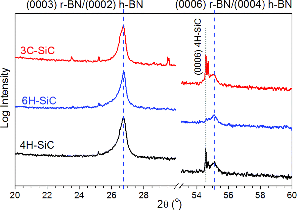 | ||
| Fig. 1 X-ray diffractograms recorded in Bragg–Brentano geometry for the films deposited on the 3C-SiC, 6H-SiC and 4H-SiC. sp2-BN deposition parameters are: T = 1500 °C, p = 70 mbar, N/B = 642, B/H2 = 0.014%, Si/B = 0.04 and NH3/H2 = 8.3%. | ||
Some asymmetry of the peak at 26.72° can be observed in all diffractograms shown in Fig. 1. This asymmetry could be explained as a consequence of the formation of small amounts of t-BN in the deposited layers. Such observation was also made in our previous work on deposition of r-BN on α-Al2O3 where it was suggested to originate from the distortion of the crystal lattice near the interface.14 Here the same explanation should be valid however, the effect of such distortion is expected to be lower due to the lower lattice mismatch between SiC and sp2-BN compared to that of the thin strained AlN buffer layer formed on α-Al2O3.
In another experiment an AlN buffer layer was deposited on (0001) 4H-SiC before the deposition of sp2-BN. Here, only a low intensity broad band was observed at lower diffraction angles in XRD (not shown here) suggesting the formation of t-BN. We have previously shown that the AlN buffer layer on (0001) α-Al2O3 must be of poor crystalline quality and/or highly strained to allow deposition of high quality r-BN on its surface.15 The AlN buffer layer grown on SiC prior the BN deposition is expected to be of high crystalline quality that will not support the growth of high quality sp2-BN and the results presented in Fig. 1 show that high quality c-axis oriented sp2-BN can be grown directly on SiC without a buffer layer. Thus, using SiC as a substrate, direct growth of sp2-BN is possible which simplifies the growth process. This growth behaviour is similar to that of AlN which can be deposited directly on SiC substrates but opposite to that of GaN which needs an AlN buffer layer when grown on SiC.16
The broad shape of the 0003 r-BN peaks in Fig. 1 is due to plotting the y-axis with the logarithmic scale together with a superposition of two peaks, as discussed above. Since 0003 peaks of r-BN exhibit a Gaussian shape it is possible to apply Scherrer's equation with the shape factor of 0.9 and FWHM of typically 0.2°. From this, the size of coherently scattering regions is estimated to be around 40 nm. Similar FWHM for the 0003 peak of r-BN is observed for all samples in this study.
TEM was employed to obtain information on the microstructure of the sp2-BN films deposited on the 6H-SiC substrate. Fig. 2a and b show the TEM images of a sample close to the interface and in the bulk of the film, respectively.
 | ||
| Fig. 2 Cross section TEM images of (a) the interface region between sp2-BN and the 6H-SiC substrate and (b) the bulk region of sp2-BN deposited on the 6H-SiC substrate. The basal planes are visible in the image. | ||
These images reveal a c-axis orientation of the deposited sp2-BN film that is in accord with the XRD measurements in Bragg–Brentano geometry. Some distortions of the crystalline structure of sp2-BN are observed near to the interface with 6H-SiC (Fig. 2a) while the crystal looks nearly perfect in the bulk of the film (Fig. 2b). Distortion of the crystalline structure near to the interface and some amount of the disordered sp2-BN on the top of the film (not shown here) are most likely the origins of the asymmetry of the r-BN/h-BN peak at 26.72° observed by XRD where superposition of two peaks is expected. Observation of this distorted region near to the interface is in line with our previous work, where the sp2-BN distorted region was observed near to the interface with an AlN buffer layer on the α-Al2O3 substrate.14 In our previous work we have shown that the sp2-BN asymmetric peak at 26.72° is formed by the superposition of two peaks, where the low intensity broad peak revealed at 26.3° is associated to the distortion of the crystal lattice i.e. formation of t-BN.15
Employing SEM, the growth rate of sp2-BN was evaluated to be in the range from 1.2 nm to 4.2 nm per minute for the B/H2 ratio of 0.014%. The uncertainty is associated to the non-uniform growth profile due to the non-rotating substrate and the fact that TEB is introduced via a liner which is not centred to the inlet of the deposition cell. The growth rate is found to be similar for all of the substrates used in this study ((111) 3C-SiC, (0001) 4H-SiC, (0001) 6H-SiC, (0001)). The average growth rate of ~4 nm min−1 on SiC substrates is also similar to that determined for the case of the α-Al2O3 substrate – 3.7 nm min−1 where the concentration of boron in the carrier gas is slightly lower – 0.01%.15 Similarity of the growth rate suggests the same growth mechanism on both SiC and α-Al2O3 substrates.
3.2. Influence of growth parameters
XRD diffractograms of layers grown on 6H-SiC at different temperatures and different N/B-ratios are shown in Fig. 3a and b, respectively. From these figures, by observing the r-BN/h-BN peaks at 26.72° and 55.07° in the 2θ scan, the optimal growth conditions on 6H-SiC are at 1500 °C and with N/B of 642. These are the same parameters previously found to be optimal for the growth on α-Al2O3 with an AlN buffer layer,15 indicating that the suggested chemical mechanism of the deposition is not affected by the change of substrate. | ||
| Fig. 3 X-ray diffractograms recorded in Bragg–Brentano geometry for the sp2-BN films deposited on 6H-SiC (a) at different temperatures (1400 °C, 1500 °C and 1600 °C; other deposition parameters are: p = 70 mbar, N/B = 642 and B/H2 = 0.014%) and (b) with different nitrogen-to-boron ratios (714, 642 and 571; other deposition parameters are: T = 1500 °C, p = 70 mbar and B/H2 = 0.014%). | ||
Fig. 4 represents diffractograms recorded from sp2-BN films grown on (000) 4H-SiC and on (0001) 4H-SiC with SiH4 being present in the reaction cell during deposition (Si/B = 0.04) and on (0001) 4H-SiC without introduction of SiH4 into the reactor even during heat-up. From these data, it is concluded that the growth of crystalline sp2-BN is achieved on (0001) 4H-SiC even without addition of SiH4 to the gas mixture, but adding a small amount of SiH4 during the temperature ramp-up and during the growth of BN increases the crystalline quality of the sp2-BN film, as manifested by an increased intensity of the 0003/0002 peak of r-BN/h-BN and the presence of a second order peak (0006/0004 peak of r-BN/h-BN). However it was not possible to deposit high quality sp2-BN on (000) 4H-SiC with the same growth recipe and XRD diffractograms did not show a peak at the 2θ angle of 26.72°.
 | ||
| Fig. 4 X-ray diffractograms recorded in Bragg–Brentano geometry for the sp2-BN films deposited on (000) 4H-SiC and on (0001) 4H-SiC with SiH4 presence in the reactor chamber during deposition and temperature ramp-up and on (0001) 4H-SiC without SiH4 addition to the gas mixture during deposition and temperature ramp-up. Other deposition parameters are: T = 1500 °C, p = 70 mbar, N/B = 642 and B/H2 = 0.014%. | ||
The observation that the presence of a minute amount of Si in the gas phase during growth increases the crystalline quality of the sp2-BN films is in line with the experiments conducted on α-Al2O3 with an AlN buffer layer.25 Moreover the difference here is the possibility to deposit the crystalline material without intentional addition of Si into the gas phase when the (0001) SiC substrate is employed while in case of the α-Al2O3 substrate Si must be present in the gas phase for crystalline sp2-BN to form.25 However, growth of high quality sp2-BN was not possible on (000) 4H-SiC even with addition of SiH4 to the gas phase and formation of t-BN can be suggested by the observation of a low intensity broad feature at angles lower than 26.72° in the XRD scan. These observations could be explained by a surface effect of Si atoms during the nucleation and the growth of sp2-BN and thus a need for Si to be present on the surface of the substrate.
3.3. Crystal structure of the films
As mentioned in the introduction and reported recently,28 it is possible to determine the crystal structure of sp2-BN from the intensity ratio of the diffraction peaks that correspond to first and second order diffraction from the sp2-BN basal planes. However, the observation of the asymmetric planes of r-BN and h-BN in XRD is a more reliable method to determine the crystalline structure of the deposited layers. Asymmetric planes of r-BN were detected and showed a twinned structure in the similar way as it was found in the case of the AlN/α-Al2O3 substrate in our previous works.14,15X-ray diffraction investigation of the (101) planes of r-BN in χ (Fig. 5a), ϕ (Fig. 5b) and 2θ (Fig. 5c) was conducted to reveal the crystalline structure of the obtained films. Fig. 5a shows the inclination of (101) with respect to the (0001) plane which is close to the calculated angle position of 77.76° (the red dashed line in Fig. 5a). Fig. 5b shows the ϕ scan of (101) planes and visualises the multiplicity of the selected plane family; six peaks are visible that are 60° separated from each other but according to the structure factor of the r-BN crystal, only 3 peaks should be present due to the 3-fold symmetry of (101) planes. This observation leads to the conclusion that the twinned crystal with a 60° rotation between twins is deposited on the 6H-SiC substrate. From these measurements together with the θ–2θ scan it is possible to evaluate both c- and a-axis parameters that are 9.99 ± 0.02 Å and 2.50 ± 0.01 Å, respectively. These values of the lattice constants are close to the r-BN bulk values which are 10.000 Å and 2.504 Å according to the powder diffraction file 045-1171 for the c- and a-axes, respectively.8 Also, by performing the ϕ-scan of the (101) planes of 6H-SiC and taking into account the θ–2θ scan, it is possible to determine the epitaxial relation between the film and substrate. In the case of r-BN on 6H-SiC this is – (0001) r-BN ∥ (0001) 6H-SiC and [100] r-BN ∥ [100] 6H-SiC, meaning that r-BN reproduces the orientation of the 6H-SiC crystal. In addition, it was not possible to observe any asymmetric peaks from h-BN in the film either due to the overlap with the tails of the intense 6H-SiC peaks in the 2θ scan which have the same inclination angle of the planes or because there is no (or low amount; transparent for XRD) h-BN inclusions in the deposited films. Planes of h-BN that could help to determine the presence of h-BN in the deposited layers were chosen to be (101) and (102) that have 2θ angles of 43.87° and 50.15° with plane inclinations with respect to the (0001) planes of 70° and 56°, respectively. These planes are chosen due to the highest relative intensity (I(0002)h-BN/I(101)h-BN = 6%; I(0002)h-BN/I(102)h-BN = 9%) compared to other asymmetric planes and because at the corresponding 2θ angles there are no peaks related to r-BN according to powder diffraction files.8 Unfortunately, these peaks overlap with tails of high intensity reflections from (10![[2 with combining macron]](https://www.rsc.org/images/entities/char_0032_0304.gif) 2) and (104) of 6H-SiC in the 2θ scan which have the same plane inclination as those chosen to reveal the presence of h-BN but have lower 2θ angles. Overlap occurs due to the use of X-ray lens that is collimating optics and not monochromatic optics. Such choice is done to achieve a higher intensity of the incidence beam since it was not possible to detect even r-BN when monochromatic optics was employed. Thus, since 0001 peaks of r-BN and h-BN overlap due to the similar spacing between the basal planes and that no asymmetric planes from h-BN were detected we conclude that there is either no formation of h-BN in our films or the amount of h-BN is insufficient to be detected by XRD. TEM investigations of the stacking sequence of the sp2-BN layers have not revealed formation of the h-BN and showed indications of rhombohedral stacking (not shown here).
2) and (104) of 6H-SiC in the 2θ scan which have the same plane inclination as those chosen to reveal the presence of h-BN but have lower 2θ angles. Overlap occurs due to the use of X-ray lens that is collimating optics and not monochromatic optics. Such choice is done to achieve a higher intensity of the incidence beam since it was not possible to detect even r-BN when monochromatic optics was employed. Thus, since 0001 peaks of r-BN and h-BN overlap due to the similar spacing between the basal planes and that no asymmetric planes from h-BN were detected we conclude that there is either no formation of h-BN in our films or the amount of h-BN is insufficient to be detected by XRD. TEM investigations of the stacking sequence of the sp2-BN layers have not revealed formation of the h-BN and showed indications of rhombohedral stacking (not shown here).
 | ||
| Fig. 5 X-Ray diffraction patterns recorded during (a) the χ scan of the sample with fixed 2θ = 42.62° that corresponds to (101) planes of r-BN, (b) the ϕ scan of the sample with fixed 2θ = 42.62° and χ = 77.76° that correspond to (101) planes of r-BN and (c) the X-Ray diffraction pattern recorded in θ–2θ geometry at fixed χ = 77.76° and ϕ = 0° angles that correspond to (101) planes of r-BN (the dash-dotted line shows the peak position). Red dashed lines in the figure show the position of the peaks calculated for the ideal lattice parameters. | ||
The same investigation was also conducted for the films deposited on the (0001) 4H-SiC substrate. Both 0003/0002 and 0006/0004 peaks of r-BN/h-BN were confined in both 2θ and ω scans, indicating a c-axis orientation. XRD investigation conducted to reveal the presence of (101) r-BN planes showed, in a similar manner as in case of the 6H-SiC substrate, 6 peaks at 77.8° in the χ scan with the 2θ angle set to 42.71°, while there were no traces of h-BN observed in XRD measurements. This suggests that in the same way as on (0001) 6H-SiC, a twinned r-BN crystal is epitaxially grown on (0001) 4H-SiC. The epitaxial relation in the case of the (0001) 4H-SiC substrate is the same as that for (0001) 6H-SiC and could be rewritten as (0001) r-BN ∥ (0001) 4H-SiC and [100] r-BN ∥ [100] 4H-SiC. Epitaxy of twinned r-BN with no detectable traces of h-BN was also observed when employing the 3C-SiC substrate. In this last case the relation of epitaxy is (0001) r-BN ∥ (111) 3C-SiC and [100] r-BN ∥ [11] 3C-SiC.
4. Conclusions
Epitaxial growth of the twinned rhombohedral boron nitride crystal is achieved on (111) 3C-, (0001) 4H- and (0001) 6H-SiC on-axis substrates without the use and need of any buffer layer. Twinned crystals of r-BN are found to be 60° rotated with respect to each other. The growth parameters that favour epitaxial growth of r-BN are: T = 1500 °C, N/B = 642 and B/H2 = 0.014% at the pressure of 70 mbar. Silicon is found to be necessary in the gas mixture for high quality r-BN to be deposited on SiC substrates. Moreover (0001) (Si-face) SiC should be used since deposition of t-BN is observed on (000) (C-face) 4H-SiC. Slight asymmetry of the 0003 peak of r-BN in XRD is explained by the distortion of the crystal structure at the interface and on the top surface of the grown film as observed in TEM. The growth rate of r-BN on SiC substrates is found to be around 4 nm min−1. All of the deposition parameters and results suggest that the growth chemistry and mechanism are the same as in for the case of using α-Al2O3 with an AlN buffer layer, while the use of SiC as the substrate eliminates the need for any buffer layer leading to a more simple deposition process.
Acknowledgements
This work was supported by the Swedish Research Council (VR: grant 621-2009-5264), Carl Tryggers Stiftelse (Nr 12:175) and the CeNano program at Linköping University. HH acknowledges support from the Swedish Government Strategic Research Area in Materials Science on Functional Materials at Linköping University (Faculty Grant SFO-Mat-LiU # 2009-00971). ZsC acknowledges the support of the Bolyai Janos research scholarship of the Hungarian Academy of Sciences.Notes and references
- Y. Kobayashi and T. Akasaka, J. Cryst. Growth, 2008, 310, 5044 CrossRef CAS PubMed.
- Y. Yokota, S. Tagawa and T. Sugino, Appl. Surf. Sci., 1999, 146, 193 CrossRef CAS.
- F. Liu, J. Yu and X. Bai, Appl. Surf. Sci., 2012, 258, 10191 CrossRef CAS PubMed.
- A. Anzai, F. Nishiyama, S. Yamanaka and K. Inumaru, Mater. Res. Bull., 2011, 46(12), 2230 CrossRef CAS PubMed.
- R. Dahal, J. Li, S. Majety, B. N. Pantha, X. K. Cao, J. Y. Lin and H. X. Jiang, Appl. Phys. Lett., 2011, 98, 211110 CrossRef PubMed.
- K. Nakamura and T. J. Sasaki, J. Solid State Chem., 2000, 154, 101 CrossRef CAS.
- Y. Kobayashi, H. Hibino, T. Nakamura, T. Akasaka, T. Makimoto and N. Matsumoto, Jpn. J. Appl. Phys., 2007, 46, 2554 CrossRef CAS.
- Joint Committee on Powder Diffraction Standards, JCPDS, Swarthmore, PA, pattern 34 – 0421; pattern 45 – 1171.
- B. E. Warren, Phys. Rev., 1941, 59, 693 CrossRef CAS.
- Y. Shi, C. Hamsen, X. Jia, K. K. Kim, A. Reina, M. Hofmann, A. L. Hsu, K. Zhang, H. Li, Z. Y. Juang, M. S. Dresselhaus, L. L. Li and J. Kong, Nano Lett., 2010, 10, 4134 CrossRef CAS PubMed.
- L. Song, L. Ci, H. Lu, P. B. Sorokin, C. Jin, J. Ni, A. G. Kvashnin, D. G. Kvashnin, J. Lou, B. I. Jakobson and P. M. Ajayan, Nano Lett., 2010, 10, 3209 CrossRef CAS PubMed.
- G. Kim, A. R. Jang, H. Y. Jeong, Z. Lee, D. J. Kang and H. S. Shin, Nano Lett., 2013, 13, 1834 CAS.
- P. Sutter, J. Lahiri, P. Zahl, B. Wang and E. Sutter, Nano Lett., 2013, 13, 276 CrossRef CAS PubMed.
- M. Chubarov, H. Pedersen, H. Högberg, V. Darakchieva, J. Jensen, P. O. Å. Persson and A. Henry, Phys. Status Solidi RRL, 2011, 5, 397 CrossRef CAS.
- M. Chubarov, H. Pedersen, H. Högberg, J. Jensen and A. Henry, Cryst. Growth Des., 2012, 12, 3215 CAS.
- R. F. Davis, M. D. Bremser, W. G. Perry and K. S. Ailey, J. Eur. Ceram. Soc., 1997, 17, 1775 CrossRef CAS.
- Z. Chen, S. Newman, D. Brown, R. Chung, S. Keller, U. K. Mishra, S. P. Denbaars and S. Nakamura, Appl. Phys. Lett., 2008, 93, 191906 CrossRef PubMed.
- G. Younes, G. Ferro, M. Soueidan, A. Brioude, V. Souliere and F. Cauwet, Thin Solid Films, 2012, 520, 2424 CrossRef CAS PubMed.
- Y. Kobayashi, T. Akasaka and T. Makimoto, J. Cryst. Growth, 2008, 310, 5048 CrossRef CAS PubMed.
- Y. Kobayashi, H. Hibino, T. Nakamura, T. Akasaka, T. Makimoto and N. Matsumoto, Jpn. J. Appl. Phys., 2007, 46, 2554 CrossRef CAS.
- S. Majety, J. Li, W. P. Zhao, B. Huang, S. H. Wei, J. Y. Lin and H. X. Jiang, Appl. Phys. Lett., 2013, 102, 213505 CrossRef PubMed.
- M. Brötzmann, H. G. Gehrke, U. Vetter and H. Hofsäss, Appl. Phys. Lett., 2010, 97, 103505 CrossRef PubMed.
- X. Li, H. Jacobson, A. Boulle, D. Chaussende and A. Henry, ECS J. Solid State Sci. Technol., 2014, 3, 75 CrossRef PubMed.
- K. A. Reinhardt and W. Kern, Handbook of silicon wafer cleaning technology, William Andrew Inc., USA, 2008, p. 24 Search PubMed.
- M. Chubarov, H. Pedersen, H. Högberg and A. Henry, CrystEngComm, 2013, 15, 455 RSC.
- J. Hassan, J. P. Bergman, A. Henry and E. Janzen, J. Cryst. Growth, 2008, 310, 4430 CrossRef CAS PubMed.
- Á. Barna, Mater. Res. Soc. Symp. Proc., 1992, 254, 3 CrossRef PubMed.
- M. Chubarov, H. Pedersen, H. Högberg, S. Filippov, J. A. A. Engelbrecht, J. O'Connel and A. Henry, Phys. B, 2014, 493, 29 CrossRef PubMed.
| This journal is © The Royal Society of Chemistry 2014 |