
 Open Access Article
 This Open Access Article is licensed under a
 Creative Commons Attribution 3.0 Unported Licence
Production of few-layer phosphorene by liquid exfoliation of black phosphorus†
Jack R.
Brent
a,
Nicky
Savjani
b,
Edward A.
Lewis
a,
Sarah J.
Haigh
a,
David J.
Lewis
*ab and
Paul
O'Brien
*ab
aSchool of Materials, The University of Manchester, Oxford Road, M13 9PL, UK. E-mail: paul.o'brien@manchester.ac.uk; david.lewis-4@manchester.ac.uk; Fax: +44 (0)161 275 4616; Tel: +44 (0)161 275 4653
bSchool of Chemistry, The University of Manchester, Oxford Road, M13 9PL, UK
First published on 8th September 2014
Abstract
We report the liquid exfoliation of black phosphorus in N-methyl-2-pyrrolidone to form few-layer phosphorene nanosheets.
Graphene is the archetypal two-dimensional material.1 Consisting of a single layer of covalently-bound sp2-hybridised carbon atoms,2,3 it has the potential to revolutionise many technologies as well as creating new ones. Graphene exhibits exceptional electronic properties,4–6 carrier transport7 and mechanical properties8 but lacks a band gap, making it of limited use in electronic devices without significant strain-engineering9 or physical modification of morphology.10 Due to its intrinsic band gap, molybdenum disulfide (MoS2) has been considered as a potentially promising semiconductor for use in optoelectronics11 and sensing12 applications despite its relatively low carrier mobility.
Phosphorene,13 the two-dimensional variant of the layered black phosphorus allotrope (Fig. 1) has attracted attention due to its p-type semiconducting properties.14Ab initio calculations predict that phosphorene has a direct thickness-dependent band gap of ca. 1.0 eV, corroborated by luminescence measurements, which is significantly larger than the band gap exhibited by bulk black phosphorus (ca. 0.3 eV).14–16 Additionally, phosphorene has high hole mobility.14 Hence, phosphorene has great potential for optoelectronic applications and use in semiconductor-based devices.
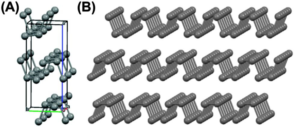 | ||
| Fig. 1 The chemical structures of the compounds in this study. (A) The orthorhombic unit cell of black phosphorus19 (a = 3.31 Å, b = 4.38 Å c = 10.50 Å, α = β = γ = 90°; space group Bmab; Crystallography Open Database ID: 1010325) which generates a layer structure comprising corrugated lamellae of phosphorus atoms held together by weak interlayer forces. (B) Three-layer phosphorene. | ||
Micromechanical cleavage (Scotch tape delamination) has been shown to reliably produce pristine, ultrathin sheets of both graphene and phosphorene, as well as inorganic graphene analogues.6,14,17 Although the method is useful for small-scale production of two-dimensional materials for fundamental research purposes it is, by its nature, not a scalable process. Two options exist to circumvent this problem. The first is by bottom-up large scale growth of two-dimensional materials, for example using chemical vapour deposition processes.18 The second is by top-down processes based on large-scale exfoliation of the bulk material precursor.
A number of successful syntheses of two-dimensional materials using liquid exfoliation have been reported by Coleman and co-workers including transition metal dichalcogenides (MoS2, WS2, MoSe2, MoTe2, TaSe2, NbSe2, NiTe2), hexagonal boron nitride (h-BN) and bismuth telluride (Bi2Te3) as well as graphene.20,21 The layered bulk solid is immersed into a liquid, typically N-methyl-2-pyrrolidone (NMP), and the two-dimensional materials are ultrasonically exfoliated. The physical basis for the exfoliation relies on an energy match between the solvent and the surface of the two-dimensional material in question balancing the energy required for exfoliation. Shear exfoliation in liquids in the presence of detergents has also recently been shown to be a viable process for the large-scale production of two-dimensional materials.22 The size of sheets as well as the concentration of the colloid may be controlled by judiciously tuning the exfoliation conditions and isolation procedures.23 Thus, liquid exfoliation routes are potentially appropriate for the large-scale production of two-dimensional nanomaterials with desired optoelectronic properties, an essential requirement for a future electronics industry based on two-dimensional materials.
In this communication, we present a simple and scalable route to few-layer phosphorene nanosheets via liquid exfoliation of black phosphorus in NMP. The phosphorene sheets are characterised by Raman spectroscopy, atomic force microscopy (AFM), transmission electron microscopy (TEM), high-angle annular dark field scanning transmission electron microscopy (HAADF-STEM), energy-dispersive X-ray (EDX) spectroscopy and EDX spectrum imaging. To the best of our knowledge this is the first report of the formation of colloidal dispersions of few-layer phosphorene nanosheets by liquid exfoliation.
To form phosphorene nanosheets, black phosphorus was exfoliated in NMP (5 mg mL−1, 0.164 mol dm−3 black phosphorus in NMP) using bath ultrasonication (820 W across four horns operating at 37 kHz frequency and 30% power) for 24 h. The temperature of the bath was maintained below 30 °C throughout using a water cooling coil. Turbid dispersions were obtained from the exfoliation step that were further purified by centrifugation to remove larger solids (see ESI† for full exfoliation and purification details). Stable dispersions were obtained from purification which are pale yellow/brown in appearance (ESI†). Silicon substrates coated with silicon dioxide of ca. 300 nm thickness (SiO2/Si) were spin-coated at 6000 rpm with a portion of the sol. Spin coating was used as the method of choice for preparation of the nanosheet-coated substrates to avoid aggregation and re-stacking of sheets. Raman spectroscopy (514 nm laser) of the spin coated SiO2/Si substrates revealed Raman bands with maxima at 361 cm−1, 438 cm−1 and 465 cm−1, corresponding to the A1g, B2g and A2g modes of few layer phosphorene, alongside the major scattering peak from the silicon substrate at 520 cm−1 (Fig. 2). These values do not suggest monolayer phosphorene was produced from exfoliation as reported by Ye and co-workers, but rather are akin to the values reported for bulk black phosphorus, suggesting that the flakes are comprised of ≥3 layers.
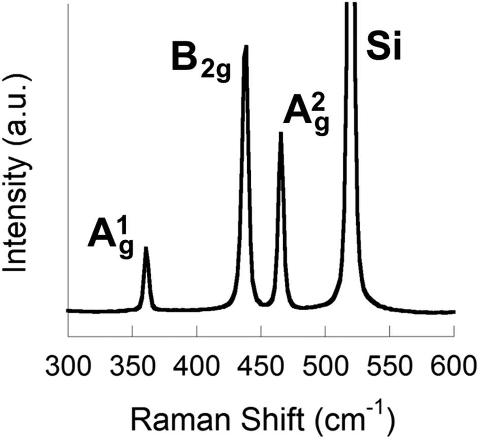 | ||
| Fig. 2 Raman spectrum of few-layer phosphorene on a SiO2/Si substrate from liquid exfoliation of black phosphorus in NMP showing the characteristic Raman bands at 361 cm−1, 438 cm−1 and 465 cm−1 assigned to the A1g, B2g and A2g modes. | ||
Atomic force microscopy (AFM) of exfoliated phosphorene on Si/SiO2 substrates revealed the presence of a range of shapes and sizes of phosphorene, with flakes as large as ca. 200 nm × 200 nm observed (Fig. 3). Height-profiling of large nanosheets revealed a thickness between ca. 3.5–5 nm (N = 11, Fig. 3A–D), with well-defined edges. Previous AFM measurements suggest that single-layer phosphorene has a thickness of ca. 0.9 nm.14 The AFM results suggest therefore that the large nanosheets predominantly consist of three to five-layer phosphorene. However, there was also strong evidence that single and bilayer phosphorene (ca. 0.9–1.6 nm thickness) is produced in the same sample, but the lateral dimensions of the nanosheets are diminished to around 20 × 20 nm (ESI†). Indeed, AFM suggests that increasing the exfoliation time to 48 h breaks down the larger flakes to mostly these smaller nanosheets that could be predominantly single and bilayer phosphorene (ESI†).
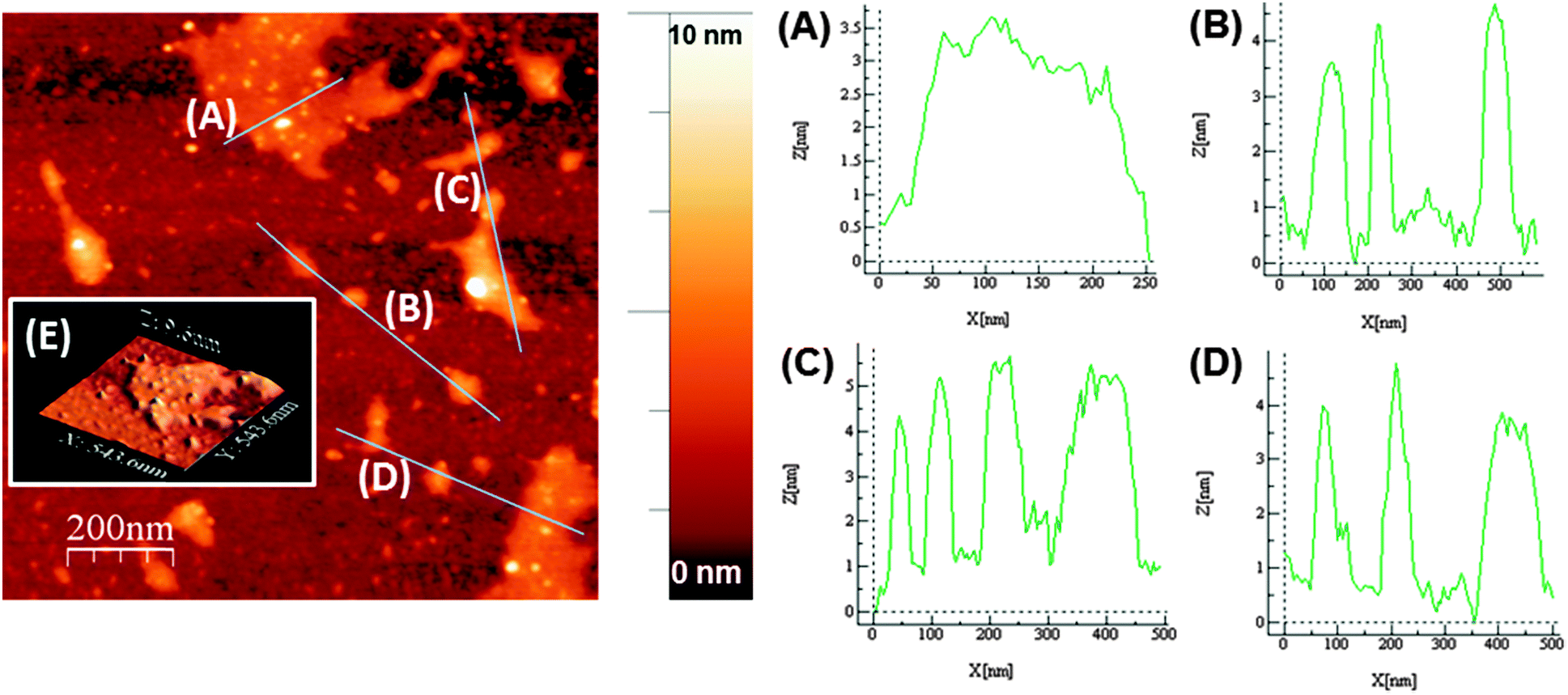 | ||
| Fig. 3 Atomic force microscopy height profile image of few-layer phosphorene sheets produced from ultrasonic exfoliation of bulk phosphorus in NMP for 24 h and spin-coated onto a SiO2/Si substrate. (A), (B), (C) and (D) show z-profiles of phosphorene flakes (N = 11) along the lines marked in the AFM relief image. Inset: (E) three-dimensional representation of the large ca. three-layer phosphorene flake observed at point (A). | ||
Raman spectroscopy was also used to analyse few-layer phosphorene exfoliated for 48 h (ESI†). Raman bands were observed at 467 cm−1, 439 cm−1 and 362 cm−1, assigned similarly to the A1g, B2g and A2g modes of few-layer phosphorene, but with 28 cm−1 difference between the A2g and B2g modes (cf. 27 cm−1 for the 24 h sample, Δ = +1 cm−1) and with the A2g mode becoming the principal band in the spectrum, both observations consistent with the thinning compared to the 24 h sample as observed by AFM.24
(Scanning) transmission electron microscopy ((S)TEM) was used to further probe the few-layer phosphorene produced by liquid exfoliation. Low magnification bright field TEM and HAADF STEM images (Fig. 4a and c and ESI†) show that the nanosheets analysed typically have lateral dimensions of the order of 100 nm. Some aggregation or re-stacking is observed to have occurred from the sample preparation with several flakes lying on top of one another due to drop casting. The crystallinity of the few-layer phosphorene was confirmed by selected area electron diffraction patterns (Fig. 4d and ESI†) and high resolution TEM (HRTEM) images (ESI†) both of which show d-spacings of 2.6, 2.2, 1.8, 1.7 and 1.3 Å which we assign to the (111), (020), (121), (024) and (117) planes, consistent with the expected crystal structure of 3–5 layer phosphorene. Notably the (002) plane is absent from the selected-area electron diffraction (SAED) pattern and HRTEM fast Fourier transform, confirming the highly two-dimensional nature of the nanosheets. Further evidence of the chemical nature and purity of the liquid exfoliated flakes is provided by energy dispersive X-ray (EDX) spectrum imaging. Elemental maps for phosphorus (Fig. 4b and ESI†), extracted from the spectrum images confirm that the phosphorus signal is strongly and undoubtedly correlated with the nanosheet location. EDX spectra (ESI†) confirm that the only other elements detected in significant levels are those associated with the TEM grid, suggesting that the nanosheets produced are of extremely high purity, consistent with their crystalline nature.
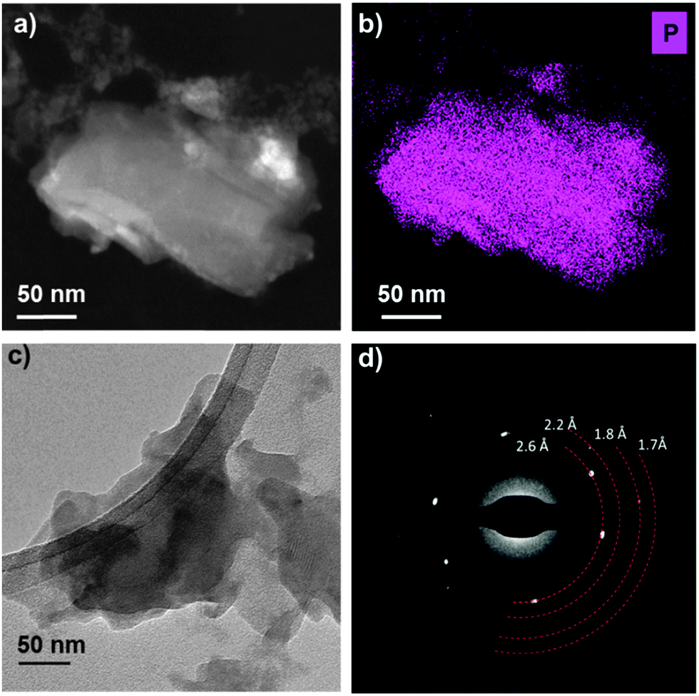 | ||
| Fig. 4 Characterisation of few-layer phosphorene sheets by electron microscopy. (a) HAADF STEM image. (b) EDX spectrum image of the same phosphorene nanosheet as in (a), showing the morphology and the distribution of phosphorus within the sheet. (c) Low magnification TEM image of a phosphorene nanosheet. (d) SAED pattern taken from the same region as in (c). The flake shown here is typical in terms of both size and morphological features. | ||
In summary, we have used the liquid exfoliation of black phosphorus in N-methyl-2-pyrrolidone to produce three to five-layer phosphorene with significant lateral dimensions, as well as smaller one-to-three layer phosphorene in the same sample. Further investigations are underway to control nanosheet size and the extent of exfoliation. With further efforts to optimise the process parameters it should be possible to produce pristine single layer phosphorene nanosheets of significant size based on this methodology. The scaleable nature of the process is important to future electronics industries based on two-dimensional direct band gap semiconductor devices.
J.R.B, N.S. and P.O.B. thank the Parker family for funding. S.J.H. and E.A.L. acknowledge funding from the Defence Threat Reduction Agency grant HDTRA1-12-1-0013 and EPSRC grants EP/K016946/1 (graphene-based membranes) and EP/G03737X/1 (NoWNano doctoral training centre).
Notes and references
- P. Miro, M. Audiffred and T. Heine, Chem. Soc. Rev., 2014, 43, 6537–6554 RSC.
- A. K. Geim, Science, 2009, 324, 1530–1534 CrossRef CAS PubMed.
- A. K. Geim and K. S. Novoselov, Nat. Mater., 2007, 6, 183–191 CrossRef CAS PubMed.
- A. H. Castro Neto, F. Guinea, N. M. R. Peres, K. S. Novoselov and A. K. Geim, Rev. Mod. Phys., 2009, 81, 109–162 CrossRef CAS.
- K. S. Novoselov, A. K. Geim, S. V. Morozov, D. Jiang, M. I. Katsnelson, I. V. Grigorieva, S. V. Dubonos and A. A. Firsov, Nature, 2005, 438, 197–200 CrossRef CAS PubMed.
- K. S. Novoselov, A. K. Geim, S. V. Morozov, D. Jiang, Y. Zhang, S. V. Dubonos, I. V. Grigorieva and A. A. Firsov, Science, 2004, 306, 666–669 CrossRef CAS PubMed.
- K. I. Bolotin, K. J. Sikes, Z. Jiang, M. Klima, G. Fudenberg, J. Hone, P. Kim and H. L. Stormer, Solid State Commun., 2008, 146, 351–355 CrossRef CAS PubMed.
- C. Lee, X. Wei, J. W. Kysar and J. Hone, Science, 2008, 321, 385–388 CrossRef CAS PubMed.
- Z. H. Ni, T. Yu, Y. H. Lu, Y. Y. Wang, Y. P. Feng and Z. X. Shen, ACS Nano, 2008, 2, 2301–2305 CrossRef CAS PubMed.
- M. Y. Han, B. Özyilmaz, Y. Zhang and P. Kim, Phys. Rev. Lett., 2007, 98, 206805 CrossRef.
- A. Kuc, N. Zibouche and T. Heine, Phys. Rev. B: Condens. Matter Mater. Phys., 2011, 83, 245213 CrossRef.
- F. K. Perkins, A. L. Friedman, E. Cobas, P. M. Campbell, G. G. Jernigan and B. T. Jonker, Nano Lett., 2013, 13, 668–673 CrossRef CAS PubMed.
- H. O. H. Churchill and P. Jarillo-Herrero, Nat. Nanotechnol., 2014, 9, 330–331 CrossRef CAS PubMed.
- H. Liu, A. T. Neal, Z. Zhu, Z. Luo, X. Xu, D. Tománek and P. D. Ye, ACS Nano, 2014, 8, 4033–4041 CrossRef CAS PubMed.
- A. N. Rudenko and M. I. Katsnelson, Phys. Rev. B: Condens. Matter Mater. Phys., 2014, 89, 201408 CrossRef.
- J. Dai and X. C. Zeng, J. Phys. Chem. Lett., 2014, 5, 1289–1293 CrossRef CAS.
- H. S. S. Ramakrishna Matte, A. Gomathi, A. K. Manna, D. J. Late, R. Datta, S. K. Pati and C. N. R. Rao, Angew. Chem., Int. Ed., 2010, 49, 4059–4062 CrossRef PubMed.
- A. Reina, X. T. Jia, J. Ho, D. Nezich, H. B. Son, V. Bulovic, M. S. Dresselhaus and J. Kong, Nano Lett., 2009, 9, 30–35 CrossRef CAS PubMed.
- R. Hultgren, N. S. Gingrich and B. E. Warren, J. Chem. Phys., 1935, 3, 351–355 CrossRef CAS PubMed.
- J. N. Coleman, M. Lotya, A. O'Neill, S. D. Bergin, P. J. King, U. Khan, K. Young, A. Gaucher, S. De, R. J. Smith, I. V. Shvets, S. K. Arora, G. Stanton, H.-Y. Kim, K. Lee, G. T. Kim, G. S. Duesberg, T. Hallam, J. J. Boland, J. J. Wang, J. F. Donegan, J. C. Grunlan, G. Moriarty, A. Shmeliov, R. J. Nicholls, J. M. Perkins, E. M. Grieveson, K. Theuwissen, D. W. McComb, P. D. Nellist and V. Nicolosi, Science, 2011, 331, 568–571 CrossRef CAS PubMed.
- Y. Hernandez, V. Nicolosi, M. Lotya, F. M. Blighe, Z. Sun, S. De, I. T. McGovern, B. Holland, M. Byrne, Y. K. Gun'Ko, J. J. Boland, P. Niraj, G. Duesberg, S. Krishnamurthy, R. Goodhue, J. Hutchison, V. Scardaci, A. C. Ferrari and J. N. Coleman, Nat. Nanotechnol., 2008, 3, 563–568 CrossRef CAS PubMed.
- K. R. Paton, E. Varrla, C. Backes, R. J. Smith, U. Khan, A. O'Neill, C. Boland, M. Lotya, O. M. Istrate, P. King, T. Higgins, S. Barwich, P. May, P. Puczkarski, I. Ahmed, M. Moebius, H. Pettersson, E. Long, J. Coelho, S. E. O'Brien, E. K. McGuire, B. M. Sanchez, G. S. Duesberg, N. McEvoy, T. J. Pennycook, C. Downing, A. Crossley, V. Nicolosi and J. N. Coleman, Nat. Mater., 2014, 13, 624–630 CrossRef CAS PubMed.
- A. O'Neill, U. Khan and J. N. Coleman, Chem. Mater., 2012, 24, 2414–2421 CrossRef.
- W. Liu, H. Nan, J. Hong, Y. Chen, C. Zhu, Z. Liang, X. Ma, Z. Ni, C. Jin and Z. Zhang, Nano Res., 2014, 7, 853–859 CrossRef.
Footnote |
| † Electronic supplementary information (ESI) available: Full description of exfoliation conditions, instrumentation used, visual appearance of black phosphorus and few-layer phosphorene dispersion; supplementary (S)TEM images, EDX spectra and EDX spectrum images. See DOI: 10.1039/c4cc05752j |
| This journal is © The Royal Society of Chemistry 2014 |