 Open Access Article
 This Open Access Article is licensed under a
 Creative Commons Attribution 3.0 Unported Licence
Bimolecular porous supramolecular networks deposited from solution on layered materials: graphite, boron nitride and molybdenum disulphide†
Vladimir V.
Korolkov
a,
Simon A.
Svatek
a,
Stephanie
Allen
b,
Clive J.
Roberts
b,
Saul J. B.
Tendler
b,
Takashi
Taniguchi
c,
Kenji
Watanabe
c,
Neil R.
Champness
d and
Peter H.
Beton
*a
aSchool of Physics & Astronomy, The University of Nottingham, Nottingham NG7 2RD, UK. E-mail: peter.beton@nottingham.ac.uk
bSchool of Pharmacy, The University of Nottingham, Nottingham, NG7 2RD, UK
cThe National Institute for Materials Science, Advanced Materials Laboratory, 1-1 Namiki, Tsukuba, Ibaraki-305-0044, Japan
dSchool of Chemistry, The University of Nottingham, Nottingham NG7 2RD, UK
First published on 23rd June 2014
Abstract
A two-dimensional porous network formed from perylene tetracarboxylic diimide (PTCDI) and melamine may be deposited from solution on the surfaces of highly oriented pyrolytic graphite (HOPG), hexagonal boron nitride (hBN) and molybdenum disulphide (MoS2). Images acquired using high resolution atomic force microscopy (AFM) operating under ambient conditions have revealed that the network forms extended ordered monolayers (>1 μm2) on HOPG and hBN whereas on MoS2 much smaller islands are observed.
Coinage-metal surfaces and highly oriented pyrolytic graphite (HOPG) have been used in many of the studies of two-dimensional supramolecular organisation which have been reported over the past decade.1–3 These conducting substrates are compatible with scanning tunnelling microscopy (STM), and have structural properties which are understood in great detail, allowing experimental studies to focus on stabilisation of networks through hydrogen bonding4–8 and metal co-ordination.9,10 An extension of these studies to other substrates, particularly non-conducting surfaces, is highly desirable and would support investigations of a much wider range of properties going beyond the determination of structural and molecular organisation. The investigation of supramolecular networks on non-metallic substrates requires the use of atomic force microscopy (AFM) rather than STM. The potential of AFM for the acquisition of high resolution images of molecular structure has been convincingly demonstrated under ultra-high vacuum (UHV) conditions,11–14 including hydrogen-bonded systems,15,16 but to date AFM images of two-dimensional supramolecular organisation with molecular resolution have only been acquired under ambient conditions for trimesic acid17 and, using a torsional tapping mode, the bimolecular network formed by PTCDI (perylene tetracarboxylic di-imide) and melamine;18 in these studies HOPG and gold, respectively, were used as substrates.
In this paper we show that, under ambient conditions, AFM images of supramolecular networks may be acquired with a resolution which is similar to that achieved using STM under the same conditions. A nanoporous honeycomb network formed from PTCDI and melamine network, previously studied on the Ag/Si(111)-surface under UHV conditions,19 and on Au(111) first under UHV20 and then from solution18,21 was chosen for this study. Recently the same network was formed on graphene multilayers grown on SiC under UHV conditions.22 Here we compare the deposition of PTCDI and melamine from solution on three layered materials, HOPG, molybdenum disulphide (MoS2) and exfoliated flakes of hexagonal boron nitride (hBN).
The molecular structures of PTCDI and melamine, together with the hydrogen-bonded PTCDI–melamine junction and the hexagonal unit cell of the resulting supramolecular structure are shown in Fig. 1. Each melamine interacts with three PTCDI molecules via a total of nine hydrogen bonds. We deposit the networks by immersion of the substrate into solutions of the molecular components which, as previous studies have shown for deposition on Au(111),18,21 leads to much larger domains than those obtained by UHV deposition.
 | ||
| Fig. 1 Chemical structure of (a) PTCDI, (b) melamine; (c) schematic of PTCDI–melamine hydrogen bonded vertex, (d) unit cells of the derived supramolecular network. | ||
Images of the networks are acquired using AFM, which for the layers deposited on graphite may be complemented by STM. In this work we use, predominantly, PeakForce tapping mode AFM, which was recently introduced by Bruker. In this mode the tip oscillates at a frequency far below resonance (2 kHz) and a force–distance curve is acquired at each pixel. The maximum force detected during the approach cycle is used as a set point which, in conjunction with a feedback loop, regulates the probe height. The values for the set point are typically in the (repulsive) range of 1–10 pN, allowing for a very low force while imaging delicate systems. As the force curve is recorded at every single pixel it is also possible to determine the spatial variation of mechanical properties, such as adhesion, of the array. AFM images were acquired in ambient conditions using standard silicon tips (Multi75Al, Multi75Al-G supplied by Budget sensors; typical spring constant, 2.8 N m−1). We have also used a Cypher AFM (Asylum Research) to acquire images (in AC mode) of some samples. STM imaging was performed utilizing tips cut from Pt/Ir (20% Ir) wire. WsXM V5.0 software was used to process and analyse all AFM images.23
The PTCDI–melamine network was prepared via adsorption in a dimethylformamide (DMF) solution at 373 K.18,21 The melamine and PTCDI concentrations were 0.66 mM and ∼0.5 μM respectively. Each sample was rinsed with 5 ml of fresh DMF and blown dry in N2-stream. The same protocol was used for all substrates.
Fig. 2 shows AFM images following molecular deposition on HOPG (purchased from NT-MDT (20 minute immersion time)). The AFM images show clearly that a regular hexagonal framework is formed on the HOPG surface with the structure and dimensions expected for the PTCDI–melamine network shown in Fig. 1. Fig. 2a shows a hexagonal array of nanopores in a single domain which extends over 250 nm (in larger area images we observe islands with dimensions up to 0.5 μm; see ESI†). The size of these domains, and the fraction of the surface covered (>90%) by the network is much greater than that achieved in previous UHV studies,19,20,22 but is comparable to those previously reported for solution deposition on Au(111).18,21 The measured lattice constant is 3.5 ± 0.1 nm, very close to the values of 3.46 nm and 3.5 nm reported for adsorption on Ag/Si(111)19 and Au(111)20,21 surfaces. A height profile extracted from a higher magnification image (Fig. 2b) is shown in the inset; the topographic height of the molecules is ∼0.1 nm. Fig. 2c shows, for comparison, an STM image of a surface prepared using the same (highly reproducible) protocol. Interestingly, there is very little difference between the resolution and image quality using these two modalities (see ESI† for additional images).
 | ||
| Fig. 2 AFM and STM scans of a PTCDI–melamine network on HOPG in air. Images (a) and (b) are topographic AFM scans. Image (c) is a constant current STM image acquired at I = 5 pA and sample voltage 0.5 V. Image (d) shows adhesion distribution of the upper half of the area in (b). Inset on image (a) shows cross-section taken along the line shown in image (b). | ||
Fig. 2d shows an adhesion map which is extracted from the force–distance curves measured during the acquisition of Fig. 2b; the adhesion is defined as the maximum attractive force during the retraction of the cantilever. This image shows stronger adhesion at the centres of the hexagonal cavities formed in the array, where the HOPG surface is exposed, with the network structure appearing as a dark honeycomb mesh (darker features correspond to lower adhesion). Similar behaviour was observed for trimesic acid monolayers adsorbed on HOPG.17 At this stage a quantitative interpretation, which requires detailed knowledge of the probe radius, is not possible. However, we include these observations to highlight the potential for AFM to provide additional modalities in future studies of host–guest interactions in supramolecular networks.
We have also successfully deposited the PTCDI–melamine network on hBN. These surfaces are prepared by exfoliating hBN flakes from small mm-sized crystals grown at the National Institute for Materials Science, and transferring them to a silicon wafer on which a 300 nm thick oxide layer has been grown. The flakes are then heated in an Ar/H2 (95![[thin space (1/6-em)]](https://www.rsc.org/images/entities/char_2009.gif) :5) atmosphere at 400 °C for 4–6 hours to remove organic residues. This process is very similar to that used by other researchers to prepare hBN substrates for use in graphene research.24,25 hBN is a layered compound with a structure similar to graphite, except that the two atom carbon basis set is replaced by two heteroatoms, boron and nitrogen. As a large band-gap semiconductor hBN is not suitable for study with STM and all images were acquired using AFM.
:5) atmosphere at 400 °C for 4–6 hours to remove organic residues. This process is very similar to that used by other researchers to prepare hBN substrates for use in graphene research.24,25 hBN is a layered compound with a structure similar to graphite, except that the two atom carbon basis set is replaced by two heteroatoms, boron and nitrogen. As a large band-gap semiconductor hBN is not suitable for study with STM and all images were acquired using AFM.
The PTCDI–melamine network could be readily formed on this substrate by immersion in the solution described above for 1 minute; this was found to be sufficient to grow an extended monolayer of the network with typical islands with widths ∼0.3 μm (see ESI†). Fig. 3a shows a large area image in which the honeycomb lattice is clearly resolved and we determine the lattice constant as 3.5 ± 0.1 nm, the same value, within experimental error as observed for the network on HOPG. Higher magnification images acquired in PeakForce tapping mode which show the honeycomb network are presented in Fig. 3b and c. In both Fig. 3a and b there are darker features with facetted edges which appear within the molecular network. These are defects in the molecular layer and tend to grow during the acquisition of AFM images in AC mode, so that after prolonged imaging the network becomes discontinuous.
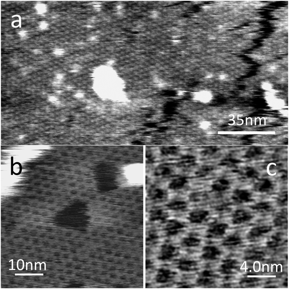 | ||
| Fig. 3 AFM scans of the PTCDI–melamine network on the hBN surface in air. Image (a) was acquired in AC mode on a Cypher AFM (Asylum Research). Images (b) and (c) were taken in PeakForce Tapping Mode. | ||
MoS2 is a layered semiconductor currently attracting interest due to its potential for integration with graphene.27 We have also demonstrated that the PTCDI–melamine network may be formed on this surface as shown in Fig. 4 (PTCDI on MoS2 has previously been studied by Ludwig et.al.26 using STM). A similar protocol is used as for the formation on HOPG and hBN, but on the MoS2 surface much smaller islands are formed. After a deposition time of 1 minute we see only islands of typical lateral dimensions of <100 nm. Increase of the immersion time to 10 minutes leads to the formation of an extended supramolecular layer with a hexagonal symmetry and a lattice constant of 3.5 ± 0.1 nm consistent with the formation of the hydrogen-bonded structure in Fig. 1. We have also tried to image this surface using STM but have not succeeded in acquiring images showing the molecular network.
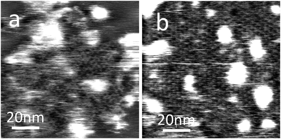 | ||
| Fig. 4 AFM images of PTCDI–melamine network on MoS2 surface after (a) 1 minute and (b) 10 minute adsorption times. | ||
The most significant difference which we identify for adsorption on MoS2 lies in the dimensions of the network. This may be due to differences in chemistry; in particular the presence of a layer of sulphur atoms at the surface may lead to stronger interactions with both environmental gaseous species, and also with the adsorbed molecules themselves. Nevertheless, our results confirm that the hydrogen-bonding which leads to the stabilisation of the honeycomb network is effective on the MoS2 surface.
The network co-exists with three dimensional features for which we cannot obtain molecular resolution; these may be due to adsorption of molecules in a non-planar configuration, or, possibly, the formation of multilayers, and are present is slightly greater concentration on the MoS2 surface. Possibly due to the smaller islands and greater disorder observed on this surface, it is more difficult to acquire images, and we have not been able to acquire adhesion maps with nm-scale MoS2 substrates (adhesion maps for hBN are included in the ESI;† these show a similar contrast to Fig. 2d). For all substrates the network structure remains sufficiently stable (when kept in a sealed vial filled with nitrogen) for further images to be obtained for over a week.
In our study we have successfully demonstrated that hydrogen-bonded supramolecular networks can be readily deposited on the surfaces of HOPG, hBN and MoS2. Importantly the structures may be resolved using AFM using conventional micromachined cantilevers. The formation of the honeycomb PTCDI–melamine network and its stability under ambient conditions is particularly important since this offers the prospect of integrating molecular recognition and host–guest interactions with a family of layered materials, including semimetals, semiconductors and insulators, which are currently receiving great attention as candidates for a new generation of optoelectronic devices.27,28
Financial support was provided by the UK Engineering and Physical Sciences Research Council (EPSRC; grants EP/K01773X/1 and EP/K005138/1).
Notes and references
- L. Bartels, Nat. Chem., 2010, 2, 87–95 CrossRef CAS PubMed.
- T. Kudernac, S. Lei, J. A. A. W. Elemans and S. De Feyter, Chem. Soc. Rev., 2009, 38, 402–421 RSC.
- A. G. Slater (née Phillips), P. H. Beton and N. R. Champness, Chem. Sci., 2011, 2, 1440 RSC.
- J. V Barth, J. Weckesser, C. Cai, P. Günter, L. Bürgi, O. Jeandupeux and K. Kern, Angew. Chem., Int. Ed., 2000, 1230–1234 CrossRef.
- S. B. Lei, C. Wang, S. X. Yin, H. N. Wang, F. Xi, H. W. Liu, B. Xu, L. J. Wan and C. L. Bai, J. Phys. Chem. B, 2001, 105, 10838–10841 CrossRef CAS.
- S. Griessl, M. Lackinger, M. Edelwirth, M. Hietschold and W. M. Heckl, Single Mol., 2002, 3, 25–31 CrossRef CAS.
- K. G. Nath, O. Ivasenko, J. A. Miwa, H. Dang, J. D. Wuest, A. Nanci, D. F. Perepichka and F. Rosei, J. Am. Chem. Soc., 2006, 128, 4212–4213 CrossRef CAS PubMed.
- D. L. Keeling, N. S. Oxtoby, C. Wilson, M. J. Humphry, N. R. Champness and P. H. Beton, Nano Lett., 2003, 3, 9–12 CrossRef CAS.
- S. Stepanow, M. Lingenfelder, A. Dmitriev, H. Spillmann, E. Delvigne, N. Lin, X. Deng, C. Cai, J. V Barth and K. Kern, Nat. Mater., 2004, 3, 229–233 CrossRef CAS PubMed.
- A. Dmitriev, H. Spillmann, N. Lin, J. V Barth and K. Kern, Angew. Chem., Int. Ed., 2003, 42, 2670–2673 CrossRef CAS PubMed.
- L. Gross, F. Mohn, N. Moll, P. Liljeroth and G. Meyer, Science, 2009, 325, 1110–1114 CrossRef CAS PubMed.
- P. Rahe, R. Lindner, M. Kittelmann, M. Nimmrich and A. Kühnle, Phys. Chem. Chem. Phys., 2012, 14, 6544–6548 RSC.
- S. Burke, J. Mativetsky, S. Fostner and P. Grütter, Phys. Rev. B, 2007, 76, 035419 CrossRef.
- S. Maier, L.-A. Fendt, L. Zimmerli, T. Glatzel, O. Pfeiffer, F. Diederich and E. Meyer, Small, 2008, 4, 1115–1118 CrossRef CAS PubMed.
- J. Zhang, P. Chen, B. Yuan, W. Ji, Z. Cheng and X. Qiu, Science, 2013, 342, 611–614 CrossRef CAS PubMed.
- A. M. Sweetman, S. P. Jarvis, H. Sang, I. Lekkas, P. Rahe, Y. Wang, J. Wang, N. Champness, L. Kantorovich and P. Moriarty, Nat. Commun., 2014, 5, 3931 CAS.
- V. V. Korolkov, S. Allen, C. J. Roberts and S. J. B. Tendler, J. Phys. Chem. C, 2012, 116, 11519–11525 CAS.
- V. V. Korolkov, N. Mullin, S. Allen, C. J. Roberts, J. K. Hobbs and S. J. B. Tendler, Phys. Chem. Chem. Phys., 2012, 14, 15909 RSC.
- J. A. Theobald, N. S. Oxtoby, M. A. Phillips, N. R. Champness and P. H. Beton, Nature, 2003, 424, 1029–1031 CrossRef CAS PubMed.
- L. M. A. Perdigão, E. W. Perkins, J. Ma, P. A. Staniec, B. L. Rogers, N. R. Champness and P. H. Beton, J. Phys. Chem. B, 2006, 110, 12539–12542 CrossRef PubMed.
- R. Madueno, M. T. Räisänen, C. Silien and M. Buck, Nature, 2008, 454, 618–621 CrossRef CAS PubMed.
- H. J. Karmel, T. Chien, V. Demers-Carpentier, J. J. Garramone and M. C. Hersam, J. Phys. Chem. Lett., 2014, 5, 270–274 CrossRef CAS.
- I. Horcas, R. Fernández, J. M. Gómez-Rodríguez, J. Colchero, J. Gómez-Herrero and A. M. Baro, Rev. Sci. Instrum., 2007, 78, 013705 CrossRef CAS PubMed.
- C. R. Dean, A. F. Young, I. Meric, C. Lee, L. Wang, S. Sorgenfrei, K. Watanabe, T. Taniguchi, P. Kim, K. L. Shepard and J. Hone, Nat. Nanotechnol., 2010, 5, 722–726 CrossRef CAS PubMed.
- M. Yankowitz, J. Xue, D. Cormode, J. D. Sanchez-Yamagishi, K. Watanabe, T. Taniguchi, P. Jarillo-Herrero, P. Jacquod and B. J. LeRoy, Nat. Phys., 2012, 8, 382–386 CrossRef CAS.
- C. Ludwig, B. Gompf, J. Petersen, R. Strohmaier and W. Eisenmenger, Z. Phys. B, 1994, 93, 365–373 CrossRef CAS.
- A. K. Geim and I. V. Grigorieva, Nature, 2013, 499, 419–425 CrossRef CAS PubMed.
- T. Georgiou, R. Jalil, B. D. Belle, L. Britnell, R. V. Gorbachev, S. V. Morozov, Y.-J. Kim, A. Gholinia, S. J. Haigh, O. Makarovsky, L. Eaves, L. a. Ponomarenko, A. K. Geim, K. S. Novoselov and A. Mishchenko, Nat. Nanotechnol., 2013, 8, 100–103 CrossRef CAS PubMed.
Footnote |
| † Electronic supplementary information (ESI) available: Additional images of network. See DOI: 10.1039/c4cc03720k |
| This journal is © The Royal Society of Chemistry 2014 |