 Open Access Article
 This Open Access Article is licensed under a Creative Commons Attribution-Non Commercial 3.0 Unported Licence
Enhanced photovoltaic performance of perovskite CH3NH3PbI3 solar cells with freestanding TiO2 nanotube array films†
Xianfeng
Gao
,
Jianyang
Li
,
Joel
Baker
,
Yang
Hou
,
Dongsheng
Guan
,
Junhong
Chen
and
Chris
Yuan
*
Department of Mechanical Engineering, University of Wisconsin Milwaukee, Wisconsin 53211, USA. E-mail: cyuan@uwm.edu
First published on 24th April 2014
Abstract
Freestanding TiO2 nanotube array films are fabricated and first applied as electrodes in perovskite CH3NH3PbI3 sensitized solar cells. The device demonstrates improved light absorption with more than 90% of light absorbed in the whole visible range and a reduced charge recombination rate, leading to a significant improvement of the photocurrent and efficiency. This study suggests a promising way of improving the conversion efficiency of perovskite solar cells through novel electrodes.
The development of organometallic halide perovskite sensitizers has attracted enormous attention on solar cell applications due to their excellent light absorbing characteristics.1 Perovskite materials were first used as sensitizers to replace traditional organic dye molecules in dye sensitized TiO2 nanocrystalline solar cells with iodide based electrolytes. These cells initially obtained an efficiency in the range of 3.7–6.5%.2 In 2012, the application of CH3NH3PbI3 led to a breakthrough in the solid-state dye sensitized solar cell (DSSC) technology, with a power conversion efficiency of 9.7% obtained using submicrometer thick mesoporous TiO2 film electrodes sensitized by perovskite CH3NH3PbI3 nanocrystals with spiro-MeOTAD as hole conductors.3 At the same time, extensive research has been conducted on the development of high efficiency solid state solar cells, with a high efficiency of 10–15% achieved.4
The primary advantage of the perovskite absorbers is their direct bandgap with large absorption coefficients over a broad range, which enables efficient light absorption in ultra-thin films. However, when only considering the light harvesting efficiency, perovskite based devices still have large potential to be improved in terms of light management. Simulated results indicate that solar cells can obtain a photocurrent of 27.2 mA cm−2 if the total photons in the 280–800 nm range could be used to generate electricity,5 while current perovskite solar cells only obtain a photocurrent of around 20 mA cm−2 on thin film solid state solar cells6 and no more than 16 mA cm−2 on iodide electrolyte based solar cells.2 The light absorption spectrum indicates that a CH3NH3PbI3 sensitized electrode appears to be more efficient to absorb light below 500 nm. The absorbance decreases gradually from 500 to 800 nm when applied on nanoparticle electrodes.6,7 Appropriate material selection and engineering designs for light management both need to be optimized to increase the photocurrent and the conversion efficiency.
In this communication, CH3NH3PbI3 sensitized perovskite solar cells were fabricated using freestanding TiO2 nanotube array electrodes. The perovskite absorber was infiltrated into the TiO2 nanotube successfully. Using the new TiO2 nanotube electrode, a significant improvement of light absorption was obtained, showing over 90% light absorption in the whole visible range. Upon combining the effects from a reduced recombination rate, the TiO2 nanotube based perovskite solar cells showed a significant increase of the power conversion efficiency over the conventional nanoparticle based solar cells. In this study, the dependence of light absorption and photovoltaic performance using iodide liquid electrolytes on the nanotube length was also investigated, while the solid state hole conductors were not employed in order to avoid variations in the pore-filling fraction, which would have otherwise complicated the electron recombination analysis.8 The device obtained a high photocurrent density of 17.9 mA cm−2 using an iodide liquid electrolyte and a conversion efficiency of 6.52%. The results indicate that TiO2 nanotubes could be promising perovskite hosts for enhancing the light absorption near the energy band edge, and can potentially pave a way for novel perovskite solid state solar cell designs and fabrications.
Here freestanding TiO2 nanotube (TNT) arrays were prepared by a two-step anodization process and then detached from the substrate by in situ field-assisted chemical dissolution.9 After transferring the freestanding nanotube arrays to FTO which was covered by a spin-coated TiO2 blocking layer, a sequential deposition approach was used to deposit the perovskite absorber into the nanotubes. PbI2 crystals were deposited into the nanotubes by spin coating of 1 M PbI2 solution in N,N-dimethylformamine. For perovskite formation, the TNT/PbI2 film was immersed into a solution of CH3NH3I in 2-propanol. In an attempt to increase the deposition of the perovskite absorber on the high aspect ratio TiO2 structure, a relatively high concentration (30 mg ml−1) of CH3NH3I was used, which tends to form CH3NH3PbI3 with a small particle size and fits the pore size of nanotube arrays. It was observed that a low concentration of CH3NH3I resulted in formation of crystals with sizes typically larger than 500 nm, which may block the pores and hamper the transformation of PbI2 inside the nanotubes. In this case, the formed perovskite crystals settled on the surface of the nanotube arrays and an inefficient sensitized electrode was produced. Further experimental details are provided in the ESI.†
The formation of perovskite in the nanotube arrays was tracked by X-ray diffraction (XRD) spectroscopy (Fig. 1). When the PbI2 crystals were deposited into the nanotube, two additional peaks appeared at approximately 12.72 and 39.52 degrees, respectively, corresponding to the reflection from (101) and (110) lattice planes of the hexagonal polytype (JCPDS 07-0235). After the transformation process from PbI2 to CH3NH3PbI3 was completed, a series of new diffraction peaks related to a tetragonal perovskite structure were observed. The strong peaks located at 14.20, 19.78, 28.23, 28.52, 29.80, 31.95, 40.61 and 43.20 degrees correspond to the reflections from (110), (112), (004), (220), (310), (312), (224) and (314) lattice planes of the tetragonal perovskite structure.2,10 No impurity peaks appeared in both steps, suggesting a complete formation of PbI2 and its controlled transformation to CH3NH3PbI3. The final perovskite absorber was well crystallized and the phase was pure.
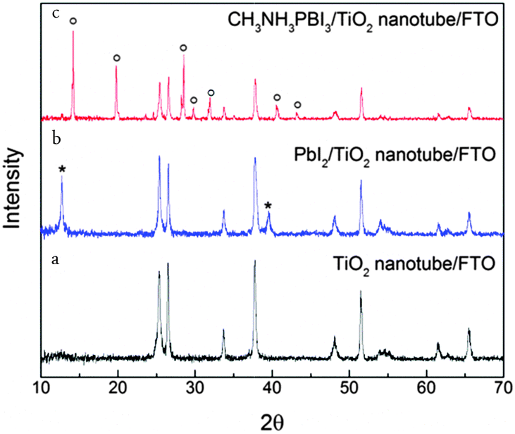 | ||
| Fig. 1 XRD spectra of pristine TiO2 nanotube electrode (a), PbI2/TiO2 nanotube electrode (b) and CH3NH3PbI3/TiO2 nanotube electrode (c). PbI2 and CH3NH3PbI3 peaks are marked with star and circle respectively. | ||
Fig. 2 compares the morphology of TiO2 nanotube electrodes before and after the perovskite dye deposition using the scanning electron microscopy (SEM) and transmission electron microscopy (TEM) images. Fig. 2a shows a typical surface morphology of the as prepared TiO2 nanotube arrays. After the two step anodization, a porous thin layer was formed on top of the nanotube arrays, which protects the nanotube arrays from top end bundling and avoids the cracks during the detachment and film transfer process (Fig. 2a). This provides a safe way to get ultrathin freestanding TiO2 nanotube array films. It is worth noting that the surface porous layer is connected with the underlayer tube opening (Fig. S1, ESI†), which would not affect the following perovskite deposition process. To investigate the dependence of the photovoltaic performance on the film thickness, three types of TiO2 nanotube array films were prepared with the tube length controlled at 2.3 μm, 4.8 μm, and 9.4 μm during the anodization process (Fig. S2, ESI†). Fig. 2b shows the cross section image of the nanotube arrays, indicating a well-controlled formation of the nanotube structure. After the perovskite absorber deposition, the nanotube structure remains intact. It was shown that some nanoparticles attached on the edge of the nanotube, and the formation of the perovskite absorber did not block the pores (Fig. 2d). Cross-sectional SEM images and TEM images (Fig. 2e and f) indicate a successful infiltration of the perovskite absorber into the nanotubes. The particle sizes of CH3NH3PbI3 were limited to less than 100 nm as controlled by the pore size of the nanotube. Cross-sectional EDS mapping (Fig. S3, ESI†) indicates that Pb and I are well distributed along the nanotube array films. Weight percentages for Pb and I from EDS elemental analysis were found to be 5.22% and 10.11%, respectively, which correspond to 0.78% and 2.47% atomic ratios and indicate a good stoichiometric ratio of Pb to I in the obtained perovskite CH3NH3PbI3.
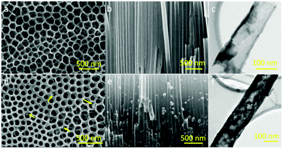 | ||
| Fig. 2 Morphology characterization of TiO2 nanotubes before and after the perovskite dye deposition. (a–c) SEM images of the top view (a), the cross section image (b) and the TEM image (c) of pristine TiO2; (d–f) SEM images of the top view (d), the cross section image (e) and the TEM image (f) of TiO2 nanotubes with CH3NH3PbI3 deposition. | ||
Fig. 3a shows a typical ultraviolet-visible (UV-Vis) absorption spectrum of CH3NH3PbI3 sensitized 4.8 μm TiO2 nanotube array electrodes. For comparison, a spectrum of photoelectrode based on TiO2 nanoparticle films with the same thickness was presented. When compared, the nanotube based electrodes have significantly larger absorbance of visible light over the whole spectrum than nanoparticle based electrodes. The nanoparticle based electrodes appeared to be efficient to absorb light below 500 nm. The absorbance decreased gradually from 500 to 800 nm, which is consistent with previously reported results.6,7 With TiO2 nanotubes as the perovskite host, the absorbance was clearly improved, especially in the long wavelength region, which could contribute to the enhanced light trapping ability of the nanotube arrays. The enhanced light absorption helps generate the photoexcited electrons and eventually improves the power conversion efficiency. Note that the scale in the figure is optical density, where an absorbance of ∼1 corresponds to ∼90% light absorption. Fig. 3b presents corresponding absorption characteristics of both nanoparticle and nanotube electrodes, where nanotube electrodes show over 90% of light absorption in almost the full visible light region. Fig. 3b also presents the dependence of the light absorption on the nanotube length. It was interesting to observe that when the TiO2 nanotube length increased from 2.3 μm to 9.4 μm, the absorption was only slightly increased in the 600–800 nm region, which could be related to the overall strong absorption of CH3NH3PbI3 sensitized TiO2 nanotube electrodes. It is worth noting that even with 2 μm nanotube arrays, the photoelectrode showed a very high light absorption. The results indicate that TiO2 nanotubes could be promising hosts for CH3NH3PbI3 solar cells with significant light absorption enhancement effects, which is important in the design of high efficiency solar devices and provides a new route to improve current perovskite solar cell technology.
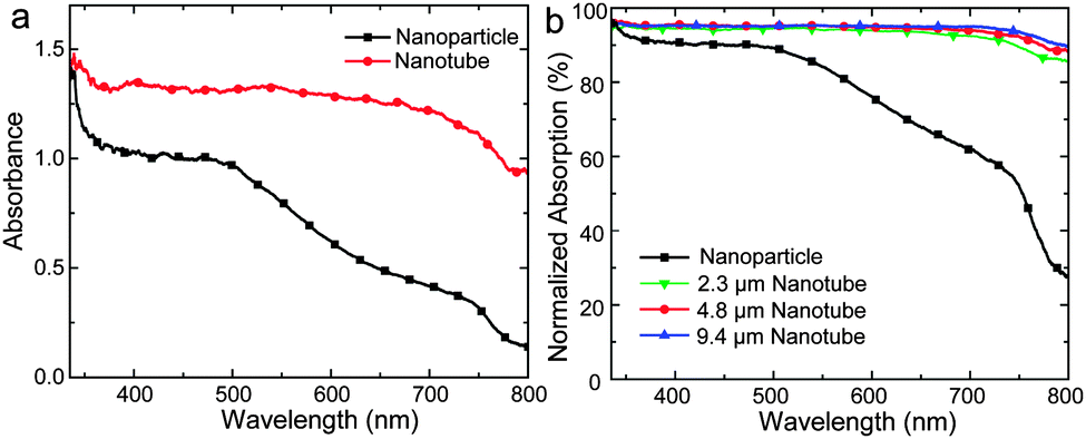 | ||
| Fig. 3 (a) UV-Vis absorption of CH3NH3PbI3 sensitized TiO2 nanoparticle and TiO2 nanotube electrode. (b) Normalized adsorption spectra as a function of TiO2 nanotube thickness compared with TiO2 nanoparticle electrodes. | ||
Fig. 4a shows the current–voltage curves of perovskite solar cells based on TiO2 nanoparticles and TiO2 nanotube array films under AM1.5 illumination. A photoconversion efficiency of 4.46% was obtained on the 4.8 μm TiO2 nanotube electrode, resulting from a photocurrent density (JSC) of 13.1 mA cm−2, an open-circuit voltage (VOC) of 0.60 V and a fill factor of 0.568. Note that the J–V curve was obtained under the reverse scan with a slow scan speed, which can minimize the efficiency deviation under different scan directions11 (Fig. S4 and Table S1, ESI†). In comparison, on the nanoparticle electrode with the same thickness, the cell efficiency was only 2.99% with a photocurrent density (JSC) of 9.5 mA cm−2, an open-circuit voltage (VOC) of 0.60 V and a fill factor of 0.525. In our tests, TiO2 nanotube based device also presented a higher incident photon-to-current efficiency (IPCE) at all effective photoresponse regions (inset of Fig. 4a). It indicates that using TiO2 nanotubes as the electrode host results in a significant photocurrent increase and thus an obvious photoconversion efficiency improvement.
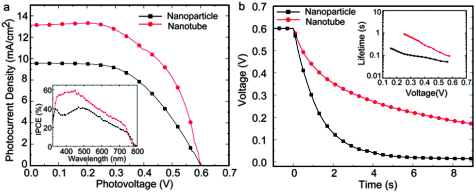 | ||
| Fig. 4 (a) J–V curves, IPCE (inset of image a), (b) open-circuit voltage decay and electron lifetimes (inset of image b) of the perovskite solar cell with nanoparticle electrodes and TNT film electrodes. | ||
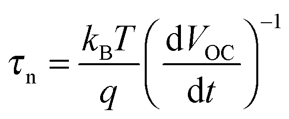
To understand the effect of TiO2 nanotube arrays on the improved photovoltaic performance, photovoltage decay measurements were performed to investigate the charge transport and recombination properties of the TiO2 nanotube based perovskite photoelectrodes (Fig. 4b). Briefly, the electron lifetimes (τn) could be derived from the photovoltage decay curve according to,12
To investigate the potential of TiO2 nanotubes as hosts for perovskite solar cells, the dependence of photovoltaic performance on the nanotube film thickness was also studied (Table 1). It was found that the device performances showed strong dependence on the nanotube length. A photoconversion efficiency of 6.52% was obtained, resulting from a 2.3 μm nanotube array film with a photocurrent density (JSC) of 17.9 mA cm−2, an open-circuit voltage (VOC) of 0.63 V and a fill factor of 0.578. The device efficiency was among the best results reported for perovskite solar cells using a liquid electrolyte.2,7 Considering that additional surface treatment was not performed and the device parameters were not fully optimized, these results were very encouraging. Table 1 shows the JSC values between 17.9 mA cm−2 and 9.73 mA cm−2 when the nanotube length changed from 2.3 μm to 9.4 μm. The VOC also decreased from 0.63 V to 0.54 V with an increase of the TiO2 nanotube length. As a result, the photoconversion efficiency decreased from 6.52% to 3.26% when the TiO2 nanotube film thickness increased from 2.3 μm to 9.4 μm.
| V OC [V] | J SC [mA cm−2] | FF | η [%] | |
|---|---|---|---|---|
| 2.3 μm | 0.63 | 17.9 | 0.578 | 6.52 |
| 4.8 μm | 0.60 | 13.1 | 0.568 | 4.46 |
| 9.4 μm | 0.54 | 9.7 | 0.624 | 3.26 |
Considering that the thickness of the TiO2 nanotube film has only a slight effect on the light absorption due to the overall high absorption ability, it was concluded that the charge collection efficiency governs the performance of the TiO2 nanotube based perovskite solar cells. Photovoltage decay measurements (Fig. S5, ESI†) showed that the photovoltage of the short nanotube array film electrode decays slower, which also presents a longer electron lifetime at equal potentials. The decreased electron lifetime of the long nanotube film suggests a high charge recombination rate and a relatively low charge collection efficiency, which consequently limits the photoconversion efficiency of the devices. IPCEs (Fig. S6, ESI†) of shorter nanotube based devices showed significant higher quantum efficiency resulting from the higher charge collection efficiency, which is consistent with the photovoltage decay measurement. Since the electron collection efficiency is close to 100% under short circuit conditions even for 20 μm thick nanotube arrays,14 it is therefore reasonable to predict that a higher recombination rate may be due to the restrained regeneration of the oxidized dyes, which is related to excited hole extraction. To get a stable performance, a low concentration I− electrolyte was used here to restrain the dye bleaching,7 which also resulted in a less effective regeneration of the oxidized dyes and led to an increased electron recombination.15 When the length of TiO2 nanotube increases, the I− diffusion pathway is prolonged, resulting in an enhanced I− depletion level inside the nanotubes, and subsequently an acceleration of the recombination.15 It should be noted that the long-term stability of nanotube based device is still not good because of the chemical instability of perovskite in the iodide electrolyte. Similar to other liquid perovskite solar cells, the degradation of the cell performance is accompanied by perovskite blenching in an iodide electrolyte. To improve their long-term stability and fully utilize the advantage of the nanotube structure, development of TiO2 nanotube based solid state perovskite solar cells is currently in progress.
In summary, perovskite solar cells based on freestanding TiO2 nanotube arrays were developed, which presented an improved photovoltaic performance with enhanced photocurrent and increased power conversion efficiency. The improvement is not only applicable to the boosting of light absorption, but also contributes to the reduced charge combination in nanotube electrodes, which suggests TiO2 nanotube arrays could be promising perovskite hosts to improve the efficiency further. It was also found that the photovoltaic performance increases with a decrease of the TiO2 nanotube film thickness, attributing to the different photoexcited charge extraction and collection efficiencies. An encouraging photovoltaic performance with a photocurrent density of 17.9 mA cm−2 and an efficiency of 6.52% was shown by the solar cell with 2.3 μm TiO2 nanotubes. Considering the feasibility of short nanotubes to provide uniform hole transport material deposition without losing light absorption enhancement features, the well aligned TiO2 nanotube array films could be promising electrodes for high efficiency solid state perovskite solar cell fabrication.
Notes and references
- B. V. Lotsch, Angew. Chem., Int. Ed., 2014, 53, 635–637 CrossRef CAS PubMed; H. J. Snaith, J. Phys. Chem. Lett., 2013, 4, 3623–3630 CrossRef; P. V. Kamat, J. Phys. Chem. Lett., 2013, 4, 3733–3734 CrossRef; J. Bisquert, J. Phys. Chem. Lett., 2013, 4, 2597–2598 CrossRef.
- J. H. Im, C. R. Lee, J. W. Lee, S. W. Park and N. G. Park, Nanoscale, 2011, 3, 4088–4093 RSC.
- H. S. Kim, C. R. Lee, J. H. Im, K. B. Lee, T. Moehl, A. Marchioro, S. J. Moon, R. Humphry-Baker, J. H. Yum, J. E. Moser, M. Gratzel and N. G. Park, Sci. Rep., 2012, 2, 591 Search PubMed.
- B. Conings, L. Baeten, C. De Dobbelaere, J. D'Haen, J. Manca and H. G. Boyen, Adv. Mater., 2014, 26, 2041–2046 CrossRef CAS PubMed; D. Liu and T. L. Kelly, Nat. Photonics, 2014, 8, 133–138 CrossRef; J. Burschka, N. Pellet, S. J. Moon, R. Humphry-Baker, P. Gao, M. K. Nazeeruddin and M. Gratzel, Nature, 2013, 499, 316–319 CrossRef PubMed; M. Liu, M. B. Johnston and H. J. Snaith, Nature, 2013, 501, 395–398 CrossRef PubMed; K. Wojciechowski, M. Saliba, T. Leijtens, A. Abate and H. J. Snaith, Energy Environ. Sci., 2014, 7, 1142–1147 Search PubMed; Q. Chen, H. Zhou, Z. Hong, S. Luo, H.-S. Duan, H.-H. Wang, Y. Liu, G. Li and Y. Yang, J. Am. Chem. Soc., 2013, 136, 622–625 CrossRef PubMed.
- G. P. Smestad, F. C. Krebs, C. M. Lampert, C. G. Granqvist, K. L. Chopra, X. Mathew and H. Takakura, Sol. Energy Mater. Sol. Cells, 2008, 92, 371–373 CrossRef CAS PubMed.
- M. M. Lee, J. Teuscher, T. Miyasaka, T. N. Murakami and H. J. Snaith, Science, 2012, 338, 643–647 CrossRef CAS PubMed.
- Y. Zhao and K. Zhu, J. Phys. Chem. Lett., 2013, 4, 2880–2884 CrossRef CAS.
- H. S. Kim, J. W. Lee, N. Yantara, P. P. Boix, S. A. Kulkarni, S. Mhaisalkar, M. Gratzel and N. G. Park, Nano Lett., 2013, 13, 2412–2417 CrossRef CAS PubMed.
- H. M. Ouyang, G. T. Fei, Y. Zhang, H. Su, Z. Jin, S. H. Xu and L. De Zhang, J. Mater. Chem. C, 2013, 1, 7498–7506 RSC.
- T. Baikie, Y. Fang, J. M. Kadro, M. Schreyer, F. Wei, S. G. Mhaisalkar, M. Graetzel and T. J. White, J. Mater. Chem. A, 2013, 1, 5628 CAS.
- K. Naoki, C. Yasuo and H. Liyuan, Jpn. J. Appl. Phys., 2005, 44, 4176 CrossRef; M. Herman, M. Jankovec and M. Topič, Int. J. Photoenergy, 2012, 2012, 151452 CrossRef PubMed.
- A. Zaban, M. Greenshtein and J. Bisquert, ChemPhysChem, 2003, 4, 859–864 CrossRef CAS PubMed.
- K. Zhu, N. R. Neale, A. Miedaner and A. J. Frank, Nano Lett., 2006, 7, 69–74 CrossRef PubMed.
- J. R. Jennings, A. Ghicov, L. M. Peter, P. Schmuki and A. B. Walker, J. Am. Chem. Soc., 2008, 130, 13364–13372 CrossRef CAS PubMed.
- A. Y. Anderson, P. R. F. Barnes, J. R. Durrant and B. C. O'Regan, J. Phys. Chem. C, 2011, 115, 2439–2447 CAS.
Footnote |
| † Electronic supplementary information (ESI) available: Experimental details, cross section images of free-standing TiO2 nanotube array, EDS mapping of TiO2/perovskite film and photovoltage decay measurement and IPCE of TiO2 nanotube devices with varied thicknesses. See DOI: 10.1039/c4cc01864h |
| This journal is © The Royal Society of Chemistry 2014 |