 Open Access Article
 This Open Access Article is licensed under a
 Creative Commons Attribution 3.0 Unported Licence
Three-dimensional periodic graphene nanostructures
Peter M.
Wilson
a,
Gilbert N.
Mbah
a,
Thomas G.
Smith
a,
Daniel
Schmidt
bc,
Rebecca Y.
Lai
ac,
Tino
Hofmann
bc and
Alexander
Sinitskii
*ac
aDepartment of Chemistry, University of Nebraska – Lincoln, Lincoln, Nebraska 68588, USA. E-mail: sinitskii@unl.edu
bDepartment of Electrical Engineering, University of Nebraska – Lincoln, Lincoln, Nebraska 68588, USA
cNebraska Center for Materials and Nanoscience, University of Nebraska – Lincoln, Lincoln, Nebraska 68588, USA
First published on 18th December 2013
Abstract
Graphene is a basic building block for many known and emerging carbon-based materials whose properties largely depend on the way how graphene is structured at the nanoscale. Synthesis of novel three-dimensional (3D) nanostructures of graphene would be an important advance for fundamental research and various applications. In this paper, we discuss the possibility of fabricating complex 3D graphene nanostructures by growing graphene on pre-synthesized nanostructured metal templates by chemical vapor deposition (CVD) and then etching away the metal. In the proof-of-concept experiments, we study this idea using two types of metal nanostructures, inverse opals and slanted nanopillar arrays grown by a glancing angle deposition (GLAD) technique. Due to the elevated temperatures used in typical CVD growth, nanostructures can be easily damaged during the growth process. Therefore, we systematically study the roles of different parameters, such as the composition, morphology and crystallinity of a nanostructured metal, as well as the CVD growth temperature and different carbon sources to grow graphene on metal nanostructures and at the same time preserve their integrity. In particular, we show that nanostructures with large crystalline domains can withstand high temperature CVD, whereas polycrystalline nanostructures, such as nanopillars grown by GLAD, suffer damage even at the low growth temperature of 500 °C. In the case of such thermally sensitive nanostructures, a careful selection of a highly reactive carbon source that could form graphene at lower temperatures becomes crucial. Furthermore, the selection of a metal is also important, as cobalt nanostructures are shown to be more resistant to thermal damage than their nickel counterparts. Finally, we could successfully remove the nanostructured metal templates to form free-standing graphene-based inverse opals and hollow graphene nanopillars. The findings presented in this paper could facilitate synthesis of other 3D graphene nanostructures.
Since the mechanical exfoliation and characterization of the electronic properties of graphene1 much research has been focused on characterizing and modifying the physical properties of graphene to better suit technological applications. Interestingly, graphene's remarkable physical properties are strongly dependent on how the graphene sheet is shaped. For example, graphene sheets could be carved to form narrow graphene nanoribbons (GNRs) that could be either metallic or semiconductive depending on their width and edge structure.2 Carbon nanotubes (CNTs), one-dimensional carbon allotropes, could be considered as rolled-up sheets of graphene.3 Similar to GNRs, CNTs could be either semiconductive or metallic depending on their diameter and chirality, i.e. the angle at which the graphene sheet is rolled.4 These two examples show that carving, twisting and rolling graphene sheets could be powerful tools to achieve graphene-based structures with new properties. This idea was extensively explored theoretically, as numerous three-dimensional (3D) graphene-based materials with intriguing properties have been proposed. These materials include periodic 3D structures comprising graphene sheets interconnected by nanotubes (“pillared graphene”),5 hybrid graphene–CNT structures6 and 3D graphene frameworks7 among others; many of these materials are discussed in a recent review.8 However, synthesis of such 3D graphene-based periodic structures remains a great challenge.
One of the foremost methods of the synthesis of graphene is chemical vapor deposition (CVD) primarily on copper or nickel substrates,9–11 whereby centimeter-scale sheets of high quality graphene can be readily grown over the surface of a catalyst metal. Although the typical CVD procedure involves growth of graphene over the surface of a flat metal foil, the CVD method could be a powerful tool to grow complex 3D graphene-based periodic structures on properly structured substrates. Fig. 1 illustrates how an arbitrarily shaped 3D metallic object (a) could serve as a backbone to grow and support a 3D graphene structure (b). Due to the complex shape and curvature the graphene coating is likely to possess structural defects that may enable etching away the metal template; whether the resulting graphene structure (c) will be free-standing or collapse could depend on many factors, such as its size, shape and etching procedure.
 | ||
| Fig. 1 General scheme of growing arbitrarily shaped graphene nanostructures: graphene is grown on a metal nanostructure (a) by CVD to form a graphene-coated metal nanostructure (b) followed by the subsequent etching of the metal leaving a free-standing graphene nanostructure (c). | ||
The goal of this study was to experimentally verify whether the growth concept presented in Fig. 1 could indeed be a viable approach to complex 3D graphene nanostructures. A control of graphene's nanoscopic morphology would afford the researcher access to any number of interesting graphene-based nanomaterials and hybrid materials. Previously, much attention has been given to optimizing graphene's micro- and nanoscale morphology for use in medical imaging, solar cells, supercapacitor electrode materials, electronic devices, and many other applications.10,12–15 Although structured CVD catalyst metals have been used to synthesize graphene of unique morphologies, they have been limited in scalability or to macroscopic structures.14,16 Thus far, no studies examining methods to deposit graphene over the surfaces of periodically arranged 3D nanostructures have been presented.
For this study we selected two different types of metal nanostructures (Fig. 2): (a) nickel inverse opals grown by electrodeposition,17–20 and (b) nickel slanted columnar thin film (SCTF) arrays grown by a glancing angle deposition (GLAD) technique.21 These nanostructures are made of the same material (Ni) and have comparable characteristic dimensions, such as an average periodicity (d) on a submicron scale and a smallest feature size t < 50 nm. However, they are prepared via completely different fabrication techniques and have entirely different geometries. Therefore, a comparison of graphene products grown on these different nanostructures by CVD under the same conditions will provide insights into the roles of the nanostructure's geometry and preparation procedure. For comparison of graphene products, we also conducted identical depositions over the surface of nickel foil.
 | ||
| Fig. 2 Metal nanostructures used in this work to grow graphene by CVD: (a) inverse opals and (b) slanted nanopillars. Top row panels show 3D schemes of these nanostructures; bottom row panels show representative SEM images of nickel inverse opals and slanted nanopillars, respectively, used in this work. Arrows show their characteristic parameters, such as an average periodicity (d) and the smallest feature size (t). | ||
In the preliminary experiments we optimized the CVD conditions to grow high-quality few-layer graphene on a nickel foil by decomposition of methane at 1000 °C,22–24 see the Experimental section for growth conditions; the high quality of graphene was confirmed by Raman spectroscopy.25,26 Then, we used exactly the same CVD procedure to grow graphene on nickel inverse opals and slanted nanopillar arrays (Fig. 3). Despite the fact that these nanostructures had the same chemical composition and comparable characteristic dimensions, the results were dramatically different. Fig. 3a and b show that the morphology of the Ni inverse opals did not visibly change during the graphene deposition. Based on the results of Raman spectroscopy the graphene grown on Ni inverse opals is multilayered, similar to graphene grown on a Ni foil under the same conditions (Fig. 4a). In contrast, when CVD growth of graphene on the nickel slanted pillars at 1000 °C was conducted, the nanostructures had melted considerably (Fig. 3d) and bore no resemblance to their original forms (Fig. 3c). Raman spectroscopy however indicated the growth of a reasonable quality multilayer graphene material (Fig. 4a).
 | ||
| Fig. 3 Growth of graphene on nickel inverse opals (a and b) and SCTFs (c and d) from methane at 1000 °C. Panels (a) and (c) show SEM images of pristine nickel nanostructures; panels (b) and (d) show the same nanostructures after graphene growth. | ||
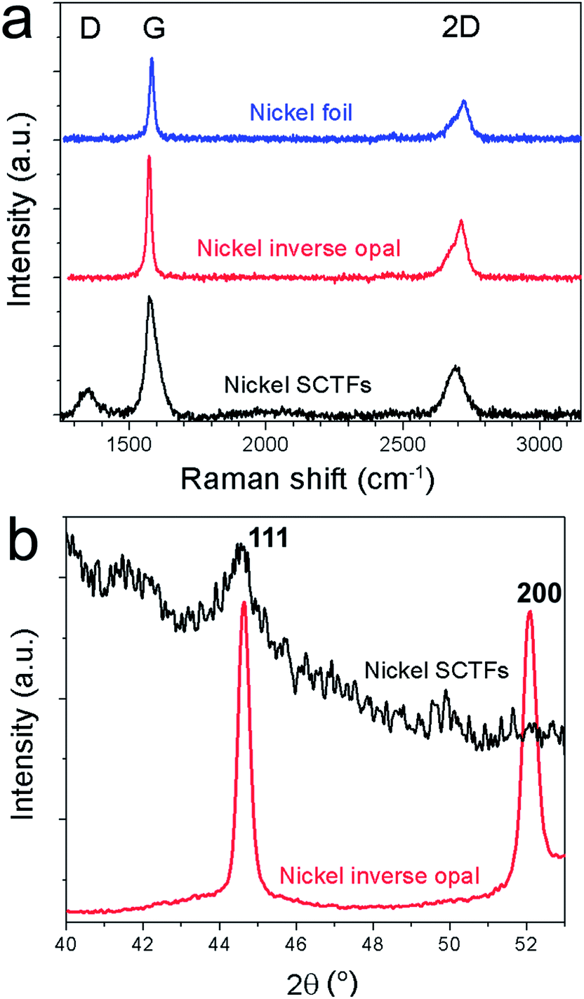 | ||
| Fig. 4 (a) Raman spectra of graphene grown from methane at 1000 °C on a nickel foil (blue), inverse opals (red) and SCTFs (black). (b) XRD spectra of nickel inverse opals (red) and nickel SCTFs scaled ×100 (black). | ||
Based on these preliminary results, the following experiments were carried out to address these questions:
(1) Why two types of nanostructures that are made of the same metal and have comparable smallest feature sizes behave so differently under the same CVD conditions?
(2) What steps could be taken to allow for graphene growth on “challenging” metal nanostructures, such as slanted nanopillars grown by GLAD, without their disintegration?
(3) Considering the ability of graphene coatings to passivate metal surfaces,27 is it possible to selectively etch the metal from graphene-coated metal nanostructures in accordance with the scheme shown in Fig. 1 to achieve free-standing graphene nanostructures?
The reason for the molten slanted pillars at temperatures much lower than the melting temperature of nickel (1455 °C) is twofold. One factor is the increased surface to volume ratio of the nanostructures, leading to dominance of surface-localized decrease in the melting temperature, which is described by the Gibbs–Thomson equation.28 However, given that the inverse opals with similar nanoscopic dimensions survived the high temperature growth, this explanation itself is not sufficient. Another reason is the low crystalline quality of the GLAD-grown nanostructures. The XRD (Fig. 4b) of the nickel inverse opals showed a relatively crystalline material, with an average domain size of about 27 nm when calculated by the Scherrer formula.29 In contrast, XRD of the nanopillar array showed that the nickel structures grown by GLAD were highly amorphous shown by the short and wide (111) peak at 2θ = 44.5°. Grain size was not estimable by XRD since the peak was wide beyond the useful limit of the Scherrer equation.29 This is in accordance with the nature of the formation of these structures, since materials grown by electrodeposition tend to have much larger crystalline domains than those grown by physical vapor deposition. Thus, in order to conduct CVD of graphene over the surface of the nanopillars, lower temperatures must be employed.
We conducted a series of experiments on growth of graphene on SCTFs from methane at different temperatures. Due to the anisotropic structure of SCTFs, the degree of structural damage to them caused by high temperature CVD could be monitored not only by SEM, but also by Mueller matrix ellipsometry (MME) as a function of the in-plane azimuth.21,30 While SEM images could be used to visualize slanted nanopillars on a micrometer scale, MME collects averaged structural information for an ∼1 × 1 cm2 SCTF area, so the SEM and ellipsometry data combined provide complete information on structural changes in SCTFs at different scales. More specifically, due to their slanted structure, nanopillar arrays exhibit an anisotropic optical response which can be detected by generalized spectroscopic ellipsometry (GSE) when measured as a function of rotational angle around the SCTF's azimuth. Although without a physical model rotation scan ellipsometry data do not give direct information regarding the nanoscopic structure of a sample, the anisotropic optical response of SCTFs has previously been characterized as being a direct result of the slanting of the nanopillars using the anisotropic Bruggeman effective medium approximation.30
An example of combined MME and SEM data is shown in Fig. 5. When the Mueller matrix components are plotted as a function of azimuthal angle “φ” for the as-grown SCTF array, they show strong angular dependencies, indicating an anisotropic structure of SCTFs (Fig. 5a, black circles). In contrast, after the CVD growth of graphene at 760 °C this optical anisotropic response is no longer observed, as the Mueller matrix components are now independent of φ, which indicates that the substrate no longer possesses an anisotropic structure. The SEM images in Fig. 5b and c also show that no slanted nanopillars survived the CVD at 760 °C, and the product is entirely molten nickel nanoparticles with graphene.
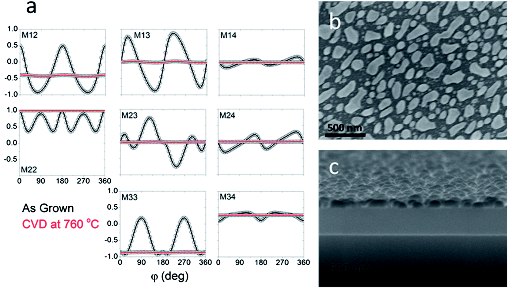 | ||
| Fig. 5 CVD of graphene on nickel SCTFs at 760 °C using methane as a carbon source. (a) Rotation scan ellipsometry of as-grown and graphene-coated nickel SCTFs measured as a function of the in-plane azimuth of the SCTF at 601 nm wavelength and 45° angle of incidence. (b, c) SEM images of nickel SCTF after graphene deposition at 760 °C: (b) top view and (c) cross-section view. | ||
We found that 760 °C is the lowest temperature at which methane decomposes over nickel under the described experimental conditions to form graphene, which is yet not low enough to ensure the structural integrity of SCTFs (Fig. 5). Therefore, in order to conduct CVD of graphene over the surface of the nanopillars, a lower growth temperature must be employed than what can be attained using a methane precursor. Many processes have performed CVD of graphene using other gaseous precursors and others have synthesized graphene using a liquid or even solid-phase carbon precursor, which has often resulted in high-quality graphene grown at relatively low temperatures.31–35 By selecting a precursor with high chemical potential, namely acetylene, it is possible to deposit graphene at significantly reduced temperatures, thereby avoiding the destruction of the nanostructures.
An array of CVD experiments on nickel foil with acetylene as a carbon source was conducted to determine the lowest growth temperature at which graphene formation occurs over nickel. The samples were analyzed by Raman spectroscopy as displayed in Fig. 6. Remarkably, it was observed that acetylene would decompose over the surface of the nickel foil at very low temperatures, at least as low as 300 °C. However, the quality of the carbon film grown was strongly dependent on the growth temperature as shown in Fig. 6b. The integrated I2D/IG ratio remained mostly constant at growth temperatures from 600 to 500 °C and then decreased to zero at 300 °C, indicating the decrease of the graphene quality. The ID/IG ratio initially increased with decreasing growth temperature until 300 °C at which point it hit a plateau approaching ∼2.0, which is close to the limit of the Tuinstra–Koenig regime due to very small graphitic domains.25,26 Based on these data, the growth temperature was chosen to be 500 °C to minimize the thermal damage to nanopillar arrays while ensuring the growth of a graphene-like product.
 | ||
| Fig. 6 (a) Raman spectra of graphene products grown at different temperatures by CVD on nickel foils with acetylene as a carbon source. (b) ID/IG (black) and I2D/IG (blue) intensity ratios versus growth temperature. | ||
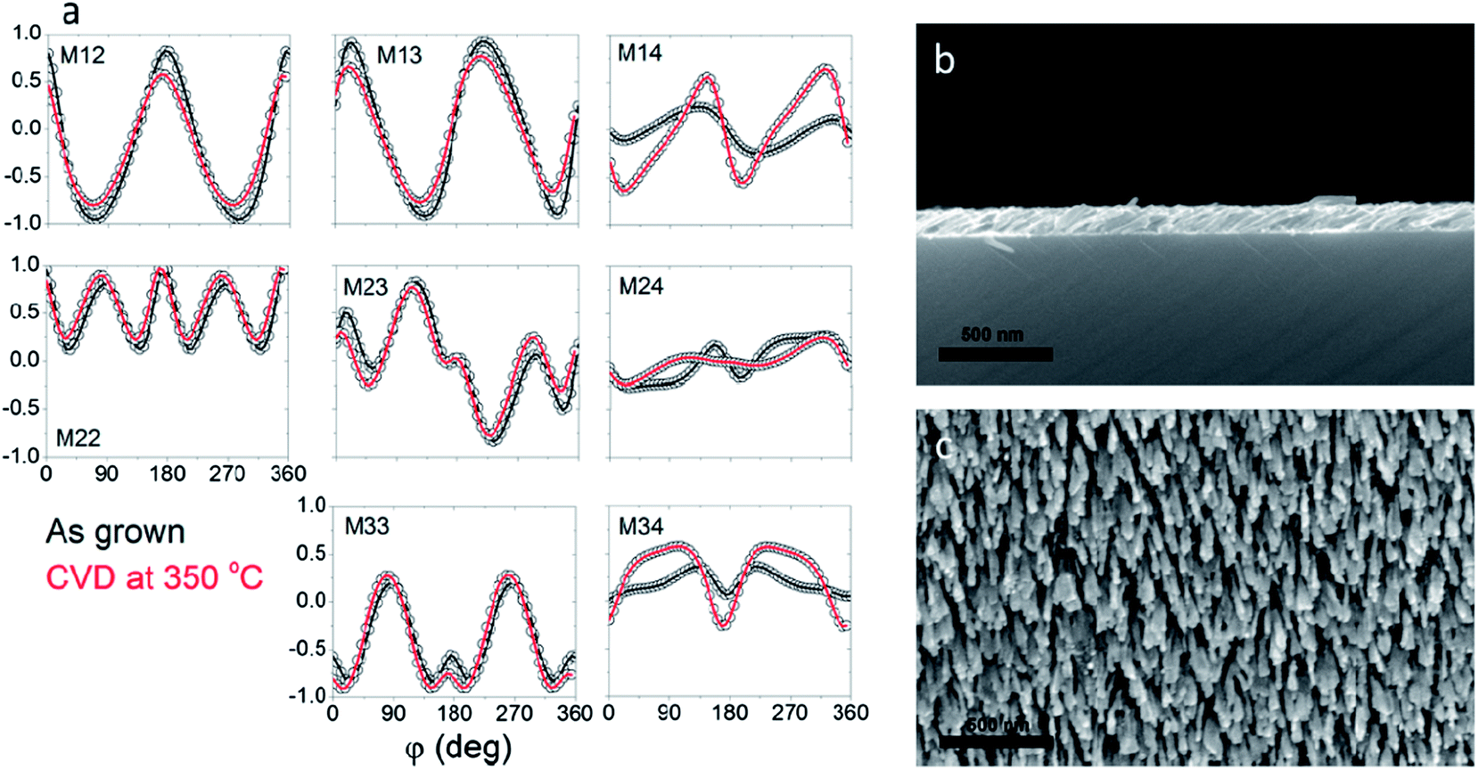
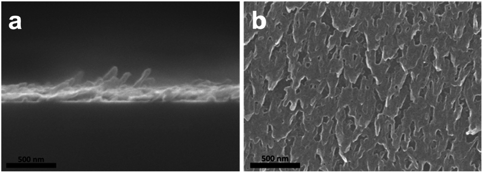
The CVD growth of graphene conducted using acetylene at 500 °C was considerably gentler to the slanted nickel pillars than the growth at higher temperatures using methane. Even so, the nanostructures were deformed in the process. Raman spectroscopy indicated the presence of a multilayered graphene product consistent with the product grown on the nickel foil. SEM imaging showed the presence of a graphene coating over the surfaces of the structures as well as the presence of some nanotubes (Fig. 7b and c). As can be seen, the pillars retained their slanted angle even after CVD, which is supported by rotation scan ellipsometry (Fig. 7a). Although the pillars coated at 500 °C also suffered from loss of anisotropy, their response is on the same order of magnitude and nearly equal in certain Mueller matrix elements, a significant improvement over the CVD conducted at 760 °C (Fig. 5a). This confirms that CVD at 500 °C preserves the slanted structure of the nanopillars more effectively than CVD at 760 °C.
 | ||
| Fig. 7 CVD of graphene on nickel (a–c) and cobalt (d–f) SCTFs at 500 °C using acetylene as a carbon source. (a, d) Rotation scan ellipsometry of as-grown and graphene-coated nickel (a) and cobalt (d) SCTFs measured as a function of rotational angle around SCTF at 601 nm wavelength and 45° angle of incidence. (b, c) SEM images of nickel SCTF after graphene deposition at 500 °C: (b) top view and (c) cross-section view. (e, f) SEM images of cobalt SCTF after graphene deposition at 500 °C: (e) top view and (f) cross-section view. | ||
Significant improvement in the quality of graphene-coated SCTFs is observed when the catalyst metal is switched to cobalt from nickel (Fig. 7d–f). Although cobalt and nickel have similar melting points (1495 and 1455 °C respectively), cobalt exhibits significantly improved thermal stability than nickel and additionally does not grow carbon nanotubes as the nickel SCTFs do. Raman spectroscopy shows that the graphene product is comparable with that grown on nickel under identical conditions. Although they are still damaged by the annealing process, the cobalt structures retain their slanted morphology much better than the nickel SCTFs as shown by both SEM images and rotation scan ellipsometry. Again, the anisotropic response is on the same order of magnitude as the as-grown SCTFs confirming the preservation of the slanted structures (Fig. 7d). Thus, when it is an option, prudent selection of material of the nanostructures could lead to improvements in the structural integrity to thermal damage.
For comparison, CVD on cobalt SCTFs was conducted at 350 °C. Raman spectroscopy confirmed the formation of a carbon product similar to that grown at 300 °C on nickel foil (Fig. 6) indicating a highly disordered carbon film. Notably SEM images showed that the cobalt SCTFs remained almost fully intact as shown in Fig. 8. This is also confirmed by ellipsometry with the anisotropic response being nearly equal in magnitude to those of the as-grown cobalt SCTFs. Thus, under the growth conditions here discussed, there is a tradeoff between retaining the original quality of the SCTFs and growth of a high quality graphene product.
 | ||
| Fig. 8 CVD of graphene on cobalt SCTFs at 350 °C using acetylene as a carbon source. (a) Rotation scan ellipsometry of as-grown and graphene-coated cobalt SCTFs measured as a function of rotational angle around SCTF at 601 nm wavelength and 45° angle of incidence. (b, c) SEM images of cobalt SCTF after graphene deposition at 350 °C: (b) top view and (c) cross-section view. | ||
In the described CVD experiments we fabricated a number of samples of graphene-coated Ni inverse opals, as well as Ni and Co SCTFs. The final question of this study is whether it is possible to selectively remove metals to form free-standing graphene nanostructures in accordance with the scheme presented in Fig. 1. The metals from the graphene-coated Ni inverse opals and Co SCTFs were removed by etching these structures with a 1 M solution of iron(III) chloride for 15 min followed by washing with water. The inverse opals, which were originally grown on Ni foils, required transfer to a SiO2/Si wafer. This was accomplished by spin-coating PMMA on an inverse opal sample, etching away the nickel from the foil and inverse opal, placing the graphene/PMMA film onto the target wafer, and removing PMMA by washing with acetone. Despite the ability of graphene coatings to passivate metal surfaces,27 Ni and Co that made up the original nanostructures had been successfully etched away, which was confirmed by energy-dispersive X-ray (EDX) spectroscopy of both samples (the EDX detection limit for transition metals in bulk materials is usually on the order of 0.1 wt%).37,38
Interestingly, after chemical etching of the nickel in the inverse opal structures, the resulting graphene inverse opals were self-supporting as demonstrated in Fig. 9. Top-view SEM images (Fig. 9a–c) of graphene inverse opal samples taken at different magnifications show a highly regular structure of periodic spherical voids in a carbon material. These voids are also seen in the side-view SEM images, such as the one shown in Fig. 9d, which demonstrates that graphene inverse opal samples have fully 3D all-carbon structure comprising a few-layer graphene framework with periodic spherical voids. It is noteworthy that the porous structures of graphene inverse opals were preserved not only during the nickel etching, but also during the transfer to Si/SiO2 substrates, washing and drying, which indicates their high mechanical stability. The mechanical stability of these structures is consistent with previous observations that graphene has remarkably high stiffness.36 To our knowledge, this is the first synthesis of free-standing graphene inverse opals, although similar periodic structures with interesting optical properties based on other carbon allotropes have been previously reported by Zakhidov et al.39
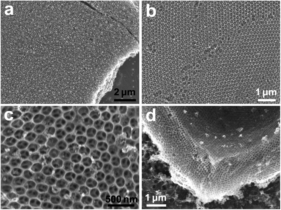 | ||
| Fig. 9 SEM images of different samples of free-standing graphene inverse opals: (a–c) top-view images and (d) side-view image. | ||
Fig. 10 shows SEM images of graphene SCTFs after cobalt etching. The majority of the SCTFs had collapsed, although some remained upright. Their collapse is likely due to the comparative mechanical instability of the slanted nanopillar morphology compared with the inverse opals. Many of the individual graphene hollow nanopillars formed by this process look flattened, thus resembling large-diameter multiwalled carbon nanotubes that could collapse along their length.40 Overall, our results demonstrate the possibility of obtaining novel 3D graphene nanostructures using properly engineered metal templates.
 | ||
| Fig. 10 SEM images of etched graphene SCTFs: (a) side and (b) top view. | ||
In summary, in this paper we demonstrate a generalized approach whereby graphene can be grown by CVD over the surface of various nanostructures. Several considerations must be taken into account when performing CVD of graphene on nanostructures. It was shown that nanostructures with high crystallinity are resilient to high temperatures and CVD using methane can be a viable option. However, for more delicate polycrystalline structures, the growth temperature must be taken into account. Methane will not suffice as a carbon source due to its high temperature of decomposition of around 760 °C. Acetylene was shown to be a much more reactive precursor which is able to decompose to form graphene of high quality at relatively low temperatures. Due to its low temperature of decomposition, acetylene is a better precursor than methane for CVD of graphene on nanostructures when thermal damage must be taken into account. Furthermore, we show that polycrystalline cobalt SCTFs are more resilient to thermal deformation than nickel SCTFs. Thus, cobalt is a preferable material for CVD of graphene on nanostructures. Finally, we demonstrate that CVD of graphene on metal nanostructures could be an effective approach to complex free-standing graphene nanostructures. Considering an enormous amount of synthetic metal nanostructures of different sizes and geometries reported elsewhere,41,42 and the possibility to create arbitrary 2D metal structures by lithography approaches,43 the described approach could yield numerous novel graphene nanostructures with interesting properties and applications.
Experimental
All chemicals were purchased from Aldrich unless otherwise specified. Monodisperse polystyrene microspheres were synthesized by emulsifier-free emulsion polymerization of styrene using potassium persulfate as an initiator.44 Two batches of microspheres with average diameters of 200 and 420 nm, respectively, and relative standard deviations σ < 5% were prepared. Colloidal crystal films were grown on nickel foil substrates (Alfa Aesar) at 50 ± 1 °C from ∼1 vol% aqueous suspensions of microspheres by the vertical deposition method.45 Nickel inverse opals were then prepared by electrodeposition of Ni between the polystyrene spheres from an aqueous solution containing 0.1 M nickel(II) chloride, 0.6 M nickel(II) sulfate, 0.1 M boric acid and 4 M ethanol at a −0.9 V potential versus the Ag/AgCl reference electrode followed by the subsequent removal of the polystyrene by immersion of the samples in toluene.17 The samples were inspected by SEM to confirm their highly regular microstructure and the absence of polystyrene residues.An 80 nm film of slanted nickel nanopillars was prepared on silicon wafers covered with 300 nm thick thermal SiO2 (SQI) by electron beam glancing angle deposition at an angle of 85°. Similarly, a 120 nm cobalt SCTF was grown on silicon. The detailed procedure has been discussed elsewhere.21
For the chemical vapor deposition on the nanostructures using methane, we found that the minimum temperature of graphene growth was 760 °C. The substrate was placed into a furnace which was evacuated to a base pressure of 6.5 mTorr. When the base pressure was achieved, 2.0 sccm of hydrogen was introduced as the furnace was raised to a temperature of either 1000 or 760 °C, after which a flow of 15.0 sccm of methane was introduced. After being held at 760 °C for 30 minutes, the furnace was switched off. When using acetylene, the process was identical with a few differences. The growth temperature was 500 °C unless otherwise noted and the flow rate of acetylene was 0.5 sccm. Due to the high reactivity of acetylene, it was found that a 10 second growth time was sufficient for graphene growth.
Prior to chemical etching of the inverse opals, the substrate was spin-coated with a 4% solution of 950 K PMMA in anisole. The substrate was then etched in 1 M iron(III) chloride (Alfa Aesar) aqueous solution overnight. The PMMA film was washed with DI water and placed onto 300 nm SiO2 on Si wafer and PMMA was then removed by washing with acetone. The cobalt SCTFs were simply etched by submersion into iron(III) chloride solution for 10 minutes followed by washing with DI water.
Raman measurements were taken using a Thermo Scientific DXR Raman microscope. Spectroscopic ellipsometry measurements were taken using a J.A. Woollam M2000 instrument with a rotating stage. SEM images were taken using a Hitachi S4700 field emission scanning electron microscope. X-ray diffraction was performed using a Rigaku D-Max/B Horizontal Q/2Q X-ray diffractometer. EDX analysis was performed using an FEI Nova NanoSEM450 field emission scanning electron microscope equipped with an Oxford Instruments EDX system.
Acknowledgements
This work was primarily funded by the Nebraska Public Power District through the Nebraska Center for Energy Sciences Research (#12-00-13) and the Center for Nanohybrid Functional Materials (NSF EPS-1004094). Partial support from the Nebraska Research Initiative and Nebraska MRSEC (NSF DMR-0820521) is also acknowledged. This research was performed in part in Central Facilities of the Nebraska Center for Materials and Nanoscience, which is supported by the Nebraska Research Initiative. The authors thank Mikhail Shekhirev for the EDX analysis of the samples.References
- K. S. Novoselov, A. K. Geim, S. V. Morozov, D. Jiang, Y. Zhang, S. V. Dubonos, I. V. Grigorieva and A. A. Firsov, Science, 2004, 306, 666–669 CrossRef CAS PubMed.
- Y. Son, M. Cohen and S. Louie, Phys. Rev. Lett., 2006, 97, 216803 CrossRef.
- A. Geim and K. Novoselov, Nat. Mater., 2007, 6, 183–191 CrossRef CAS PubMed.
- P. Avouris, Z. Chen and V. Perebeinos, Nat. Nanotechnol., 2007, 2, 605–615 CrossRef CAS PubMed.
- G. Dimitrakakis, E. Tylianakis and G. Froudakis, Nano Lett., 2008, 8, 3166–3170 CrossRef CAS PubMed.
- E. Sheka and L. Chernozatonskii, J. Comput. Theor. Nanosci., 2010, 7, 1814–1824 CrossRef CAS PubMed.
- M. Wu, X. Wu, Y. Pei, Y. Wang and X. Zeng, Chem. Commun., 2011, 47, 4406–4408 RSC.
- A. Ivanovskii, Russ. Chem. Rev., 2012, 81, 571–605 CrossRef PubMed.
- X. Li, W. Cai, J. An, S. Kim, J. Nah, D. Yang, R. Piner, A. Velamakanni, I. Jung, E. Tutuc, S. K. Banerjee, L. Colombo and R. S. Ruoff, Science, 2009, 324, 1312–1314 CrossRef CAS PubMed.
- H. Bi, F. Huang, J. Liang, Y. Tang, X. Lu, X. Xie and M. Jiang, J. Mater. Chem., 2011, 21, 17366–17370 RSC.
- R. Addou, A. Dahal, P. Sutter and M. Batzill, Appl. Phys. Lett., 2012, 100, 021601 CrossRef PubMed.
- W. Chen and L. Yan, Nanoscale, 2011, 3, 3132–3137 RSC.
- Y. Chen, F. Guo, Y. Qiu, H. Hu, I. Kulaots, E. Walsh and R. H. Hurt, ACS Nano, 2013, 7, 3744–3753 CrossRef CAS PubMed.
- T. Kato and R. Hatakeyama, Nat. Nanotechnol., 2012, 7, 651–656 CrossRef CAS PubMed.
- S. Crowder, D. Prasai, R. Rath, D. Balikov, H. Bae, K. Bolotin and H. Sung, Nanoscale, 2013, 5, 4171–4176 RSC.
- Z. Chen, W. Ren, L. Gao, B. Liu, S. Pei and H.-M. Cheng, Nat. Mater., 2011, 10, 424–428 CrossRef CAS PubMed.
- K. Napolskii, A. Sinitskii, S. Grigoriev, N. Grigorieva, H. Eckerlebe, A. Eliseev, A. Lukashin and Y. Tretyakov, Phys. B, 2007, 397, 23–26 CrossRef CAS PubMed.
- P. N. Bartlett, M. A. Ghanem, I. S. El Hallag, P. de Groot and A. Zhukov, J. Mater. Chem., 2003, 13, 2596–2602 RSC.
- X. Yu, Y. Lee, R. Furstenberg, J. White and P. Braun, Adv. Mater., 2007, 19, 1689–1692 CrossRef CAS.
- J. Hilhorst, V. Abramova, A. Sinitskii, N. Sapoletova, K. Napolskii, A. Eliseev, D. Byelov, N. Grigoryeva, A. Vasilieva, W. Bouwman, K. Kvashnina, A. Snigirev, S. Grigoriev and A. Petukhov, Langmuir, 2009, 25, 10408–10412 CrossRef CAS PubMed.
- D. Schmidt, A. Kjerstad, T. Hofmann, R. Skomski, E. Schubert and M. Schubert, J. Appl. Phys., 2009, 105, 113508 CrossRef PubMed.
- A. Obraztsov, E. Obraztsova, A. Tyurnina and A. Zolotukhin, Carbon, 2007, 45, 2017–2021 CrossRef CAS PubMed.
- A. Reina, X. Jia, J. Ho, D. Nezich, H. Son, V. Bulovic, M. Dresselhaus and J. Kong, Nano Lett., 2009, 9, 30–35 CrossRef CAS PubMed.
- K. Kim, Y. Zhao, H. Jang, S. Lee, J. Kim, K. Kim, J. Ahn, P. Kim, J. Choi and B. Hong, Nature, 2009, 457, 706–710 CrossRef CAS PubMed.
- A. C. Ferrari, J. C. Meyer, V. Scardaci, C. Casiraghi, M. Lazzeri, F. Mauri, S. Piscanec, D. Jiang, K. S. Novoselov, S. Roth and A. K. Geim, Phys. Rev. Lett., 2006, 97, 187401 CrossRef CAS.
- A. C. Ferrari, Solid State Commun., 2007, 143, 47–57 CrossRef CAS PubMed.
- S. Chen, L. Brown, M. Levendorf, W. Cai, S.-Y. Ju, J. Edgeworth, X. Li, C. W. Magnuson, A. Velamakanni, R. D. Piner, J. Kang, J. Park and R. S. Ruoff, ACS Nano, 2011, 5, 1321–1327 CrossRef CAS PubMed.
- C. Jackson and G. Mckenna, J. Chem. Phys., 1990, 93, 9002–9011 CrossRef CAS PubMed.
- B. D. Cullity and S. R. Stock, Elements of X-Ray Diffraction, Prentice Hall, 2001 Search PubMed.
- D. Schmidt, E. Schubert and M. Schubert, Appl. Phys. Lett., 2012, 100, 011912 CrossRef PubMed.
- G. Ruan, Z. Sun, Z. Peng and J. M. Tour, ACS Nano, 2011, 5, 7601–7607 CrossRef CAS PubMed.
- X. Wan, K. Chen, D. Liu, J. Chen, Q. Miao and J. Xu, Chem. Mater., 2012, 24, 3906–3915 CrossRef CAS.
- R. S. Weatherup, B. Dlubak and S. Hofmann, ACS Nano, 2012, 6, 9996–10003 CrossRef CAS PubMed.
- Y. Xue, B. Wu, L. Jiang, Y. Guo, L. Huang, J. Chen, J. Tan, D. Geng, B. Luo, W. Hu, G. Yu and Y. Liu, J. Am. Chem. Soc., 2012, 134, 11060–11063 CrossRef CAS PubMed.
- S.-M. Yoon, W. M. Choi, H. Baik, H.-J. Shin, I. Song, M.-S. Kwon, J. J. Bae, H. Kim, Y. H. Lee and J.-Y. Choi, ACS Nano, 2012, 6, 6803–6811 CrossRef CAS PubMed.
- T. J. Booth, P. Blake, R. R. Nair, D. Jiang, E. W. Hill, U. Bangert, A. Bleloch, M. Gass, K. S. Novoselov, M. I. Katsnelson and A. K. Geim, Nano Lett., 2008, 8, 2442–2446 CrossRef CAS PubMed.
- P. R. Buseck and J. P. Bradley, Electron Beam Studies of Individual Natural and Anthropogenic Microparticles: Compositions, Structures, and Surface Reactions, in Heterogeneous Atmospheric Chemistry, Geophysical Monograph, American Geophysical Union, 1982, vol. 26, pp. 57–76 Search PubMed.
- S. J. B. Reed, Electron Microprobe Analysis and Scanning Electron Microscopy in Geology, Cambridge University Press, 2nd edn, 2010 Search PubMed.
- A. Zakhidov, R. Baughman, Z. Iqbal, C. Cui, I. Khayrullin, S. Dantas, I. Marti and V. Ralchenko, Science, 1998, 282, 897–901 CrossRef CAS.
- N. G. Chopra, L. X. Benedict, V. H. Crespi, M. L. Cohen, S. G. Louie and A. Zettl, Nature, 1995, 377, 135–138 CrossRef CAS.
- Y. Xia, P. Yang, Y. Sun, Y. Wu, B. Mayers, B. Gates, Y. Yin, F. Kim and H. Yan, Adv. Mater., 2003, 15, 353–389 CrossRef CAS.
- A. Schwartzberg and J. Zhang, J. Phys. Chem. C, 2008, 112, 10323–10337 CAS.
- Y. Xia, J. Rogers, K. Paul and G. Whitesides, Chem. Rev., 1999, 99, 1823–1848 CrossRef CAS PubMed.
- J. W. Goodwin, J. Hearn, C. C. Ho and R. H. Ottewill, Colloid Polym. Sci., 1974, 252, 464–471 CAS.
- P. Jiang, J. F. Bertone, K. S. Hwang and V. L. Colvin, Chem. Mater., 1999, 11, 2132–2140 CrossRef CAS.
| This journal is © The Royal Society of Chemistry 2014 |