Recent advances in the growth of germanium nanowires: synthesis, growth dynamics and morphology control
Colm
O'Regan
ab,
Subhajit
Biswas
ab,
Nikolay
Petkov
ab and
Justin D.
Holmes
*ab
aMaterials Chemistry and Analysis Group, Department of Chemistry and the Tyndall National Institute, University College Cork, Ireland. E-mail: j.holmes@ucc.ie; Fax: +353 (0)21 4274097; Tel: +353 (0)21 4903608
bCentre for Research on Adaptive Nanostructures and Nanodevices (CRANN), Trinity College Dublin, Dublin 2, Ireland
First published on 11th October 2013
Abstract
One-dimensional semiconductor nanostructures have been studied in great depth over the past number of decades as potential building blocks in electronic, thermoelectric, optoelectronic, photovoltaic and battery devices. Silicon has been the material of choice in several industries, in particular the semiconductor industry, for the last few decades due to its stable oxide and well documented properties. Recently however, Ge has been proposed as a candidate to replace Si in microelectronic devices due to its high charge carrier mobilities. A number of various ‘bottom-up’ synthetic methodologies have been employed to grow Ge nanowires, including chemical vapour deposition, thermal evaporation, template methods, supercritical fluid synthesis, molecular beam epitaxy and solution phase synthesis. These bottom-up methods afford the opportunity to produce commercial scale quantities of nanowires with controllable lengths, diameters and crystal structure. An understanding of the vapour–liquid–solid (VLS) and vapour–solid–solid (VSS) mechanism by which most Ge nanowires are produced, is key to controlling their growth rate, aspect ratio and morphology. This article highlights the various bottom-up growth methods that have been used to synthesise Ge nanowires over the past 5–6 years, with particular emphasis on the Au/Ge eutectic system and the VLS mechanism. Thermodynamic and kinetic models used to describe Ge nanowire growth and morphology control will also be discussed in detail.
 Colm O'Regan | Colm O'Regan is currently a PhD student in the Materials Chemistry & Analysis Group, led by Prof. Justin Holmes, at University College Cork, Cork, Ireland. Colm's research primarily focuses on manipulating the growth kinetics of semiconductor nanowires, with a heavy emphasis on using electron microscopy techniques to elucidate nanowire growth mechanisms. |
 Subhajit Biswas | Subhajit Biswas studied Physics at Jadavpur University, India. He carried out doctoral research at the ‘Indian Association for the Cultivation of Science’, Jadavpur University, Kolkata. In 2008 he received his PhD in Materials Science for the work on synthetic methods and physical properties of nanostructured materials. He is currently working as a Senior Postdoctoral Fellow in the Department of Chemistry & Tyndall National Institute, UCC, Cork, Ireland under the supervision of Prof. Justin D Holmes. His current research interests include the exploration of the kinetic and thermodynamic aspects of 1D growth for nanowire defect engineering. |
 Nikolay Petkov | Nikolay Petkov graduated from Sofia University in 1998 and then completed his PhD in Physical and Materials Chemistry from the University of Munich (LMU) in 2004. He was a Postdoctoral Fellow at LMU and University College Cork (UCC) before becoming chief technologist at the Electron Microscopy and Analysis Facility at Tyndall National Institute. At Tyndall, he is leading research in advanced electron microscopy for analysis of semiconductor materials and devices. His research interests are in situ and correlative electron microscopy, tomographic imaging, materials processing and self-assembly. He has authored and co-authored over 60 peer-review publications, several reviews and book chapters. |
 Justin D. Holmes | Justin D. Holmes is Professor of Nanochemistry at University College Cork (UCC), Ireland. His research is focused on the synthesis, assembly and characterisation of nanoscale materials for electronic, energy, environmental and catalytic applications. He is Group Leader of the Materials Chemistry & Analysis Group at the Tyndall National Institute in Cork and a Principal Investigator within the Centre for Adaptive Nanostructures and Nanodevices (CRANN), based at Trinity College Dublin (TCD). |
1. Introduction
One-dimensional semiconductor nanowires have stimulated much interest in the last decade due to their potential use as building blocks for assembling nanoscale devices and architectures.1,2 They also possess unique properties compared to their bulk counterparts, such as quantum confinement, allowing them to be utilised in functional optoelectronic and photovoltaic devices.3,4 Significantly, semiconductor nanowires have already shown promise in several fields such as construction,5 energy conversion,6 electronics1,4,7,8 and photonics9 and will likely continue to lead the way for the development of future applications. The continued miniaturisation of electronic components in accordance with Moore's Law10 and the imminent approach of device scaling limitations have made research into semiconducting nanowires even more imperative.Silicon has been the material of choice for the above applications, particularly the microelectronics industry, for the last number of decades. Hence, research into materials that are compatible with current Si-based technology is considered a significant requirement in nanoelectronics. Like Si, Ge is a Group 14 semiconductor material and as such, it shares several properties in common with Si, such as a diamond cubic crystal structure. Germanium also exhibits certain properties that are superior to those of Si, including a higher charge carrier mobility11 and a larger Bohr exciton radius. For this reason, interest in Ge nanowires has flourished in the last few years12,13 as research groups and industry contemplate the necessary migration away from Si in order to improve functionality in electronic devices. Ge has already been shown to have potential use in applications such as lithium-ion batteries,14–16 field effect transistors (FETs),17,18 memory applications,19–21 photovoltaics22,23 and nanoelectromechanical systems (NEMS).24,25 Ge nanowires have also been used as a means of studying dopant location26 as well as strain,27,28 transport modulation29 and band offset efficiency30 in the form of core–shell nanowires. Finally, surface morphologies greatly affect nanowire properties due to the high surface to volume ratio, thus research into the functionalisation of germanium nanowire surfaces31–35 has resulted in further development and a better understanding of the potential of these materials.
Current bottom-up epitaxial methods make use of the classic vapour–liquid–solid (VLS) mechanism to synthesise one-dimensional nanostructures, where a liquid catalytic seed is employed for unidirectional, diameter-controlled nanowire growth.36–41 In order to take advantage of the unique optical and electrical properties experienced on the nanoscale, strict control over the diameter and length of semiconductor nanowires is required. This control is difficult to achieve unless colloidal metal nanoparticles/seeds with tight diameter distributions are used. Understanding the important concepts and parameters that participate in a bottom-up nanowire growth mechanism, such as nucleation, supersaturation, preferential deposition and interfacial energies, opens up the possibilities of controlling the morphology of Ge nanowires to a high degree; an obvious prerequisite if they are going to be integrated into future devices. Consequently, this article aims to review the progress of Ge nanowire research over the past 5–6 years, focusing on the various methods utilised to control wire morphology and growth. A brief review of the recent synthetic methods employed to grow Ge nanowires will also be presented. Subsequently, various mechanisms of growth will be discussed with a particular emphasis on Au/Ge eutectic alloy systems.
2. Nanowire synthesis
Various synthetic methods have been employed to grow one-dimensional nanowires,8,13 the majority of which utilise the VLS mechanism and its various derivatives such as vapour-solid-solid (VSS) and solution–liquid–solid (SLS). An example of the SLS method is given in Fig. 1.42 These approaches include bottom-up techniques such as metal promoted vapour phase growth, metal assisted growth in liquids, non-metal gas phase growth and template synthesis. Top-down methods, which include electron beam and focused ion beam lithography, are also commonly employed in the production of well-ordered arrays of semiconductor nanowires. This section will review the synthetic methods commonly employed to grow Ge nanowires, with a focus on the bottom-up approaches. Specifically, the most widely used catalyst-based methods carried out in vapour, liquid and supercritical media will be discussed in addition to non-catalyst assisted methods. As top-down methods have not been widely utilised to generate Ge nanowires, they will not be discussed in this review. However, a detailed discussion on the top-down fabrication of semiconductor nanowires, particularly Si, has previously been reported by Hobbs et al.43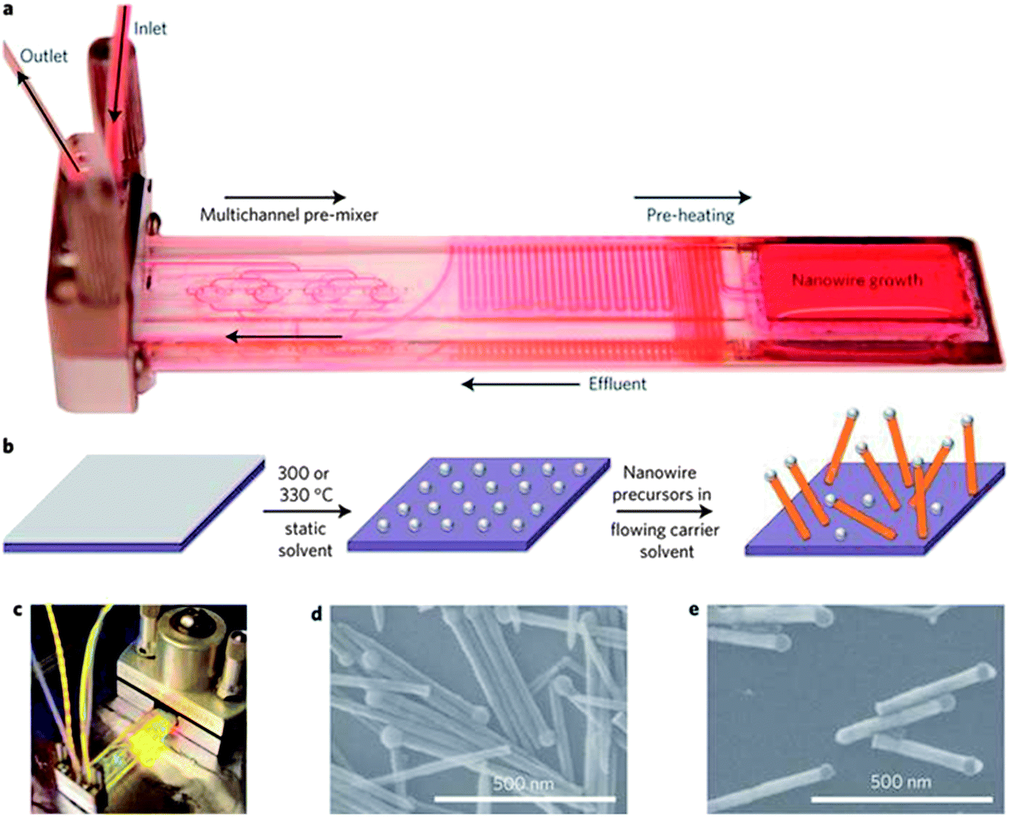 | ||
| Fig. 1 Flow-SLS growth. (a) Custom microfluidic chip filled with Rhodamine 6G dye to visualize chip zones. (b) Schematic of flow-SLS synthesis of semiconductor nanowires grown from substrates held in flow. (c) Flow-SLS chip mounted in a stainless-steel holder, as during growth (d) and (e) SEM images of CdSe (d) and ZnSe (e) nanowires grown in flow at 330 °C from 10 and 2 nm thick Bi layers, respectively. “Reprinted by permission from Macmillan Publishers Ltd: [Nat. Nanotechnol.]42 copyright 2013.” | ||
2.1. Seeded growth in vapour and liquid media
The most frequently used method for growing 1D semiconductor nanowires (including Ge) is the application of a metal catalyst particle in a liquid phase which promotes unidirectional growth via a three phase VLS mechanism44 and can be performed within vapour, liquid or supercritical fluid (SCF) environments. Vapour and liquid-based growth of Ge nanowires consists of any method where the Ge precursor is in either vapour and liquid form and include techniques such as chemical vapour deposition (CVD),45–50 metal–organic chemical vapour deposition (MOCVD),51,52 molecular beam epitaxy,53–55 template methods56,57 and various evaporation methods such as electron beam evaporation58,59 and thermal evaporation.60,61 Alternatively, liquid/solution (see Fig. 1)14,52,62–67 and SCF68–72 based methods involve the introduction of precursors in liquid and supercritical media respectively. The key mechanism involved in most of these processes is analogous to the VLS mechanism first proposed by Wagner and Ellis73 for the growth of Si nanowhiskers from SiCl4. This growth mechanism is compared to its solid-phase analogue, the VSS mechanism, in Fig. 2.74 The VLS mechanism was based on the observations that metal impurities (seeds) were required for nanowire growth and that small amounts of the impurity were present at the tips of the wires. The diagram shown in Fig. 2 conveys the VLS and VSS growth of Ge nanowires from Au seeds using a Ge2H6 precursor vapour. The VSS growth model will be discussed briefly in the next section. The VLS mechanism utilises liquid seeds (metal impurities) to promote nanowire growth via a supersaturation mediated process with a vapour precursor. Supersaturation, the difference in chemical potential (Δμ) between Ge in the vapour phase and solid semiconductor phase, is the driving force behind VLS-nanowire growth; where 2D ledge nucleation at the triple phase boundary (TPB) and subsequent nanowire growth occurs when the kinetic barrier to nucleation is overcome.75 Generally, participation of the VLS mechanism for nanowire growth can be identified in electron microscopy by the presence of a heavier seed at the tip of the nanowire, as these methods are characterised by the use of seeds to promote nanowire growth.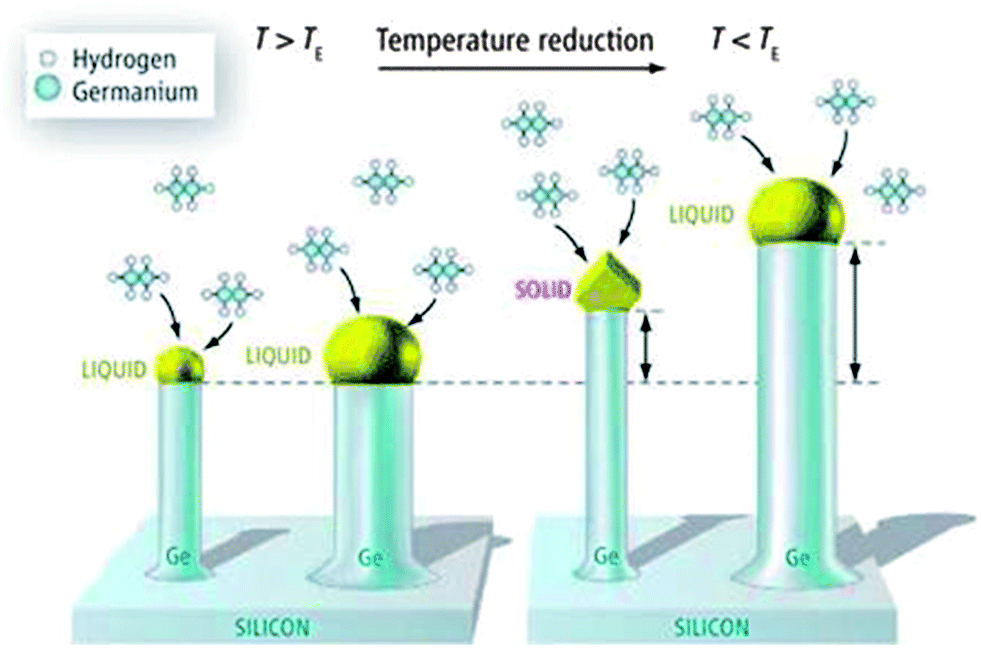 | ||
| Fig. 2 Representation of VLS and VSS mechanisms for growing Ge NWs. Above TE (left), the nanowires have a liquid gold cap and grow via VLS growth. Below TE (right), the cap of relatively thick nanowires is liquid, whereas the cap of relatively thin nanowires becomes a crystalline solid. “From ref. 74, reprinted with permission from AAAS.” | ||
CVD is the most commonly employed bottom-up method used to synthesise Ge nanowires. The standard procedure is to introduce a gaseous Ge precursor, typically GeCl4, GeH4 or Ge2H6, into a system containing a Si substrate that has been coated with a gold film or Au nanoparticles.76–78 A carrier gas such as H2/Ar is employed to transport the precursor to the reaction site and to provide an oxygen free, reducing environment. Variations on the standard CVD method include using substrates other than Si, such as Ti,79 the use of alternative precursors, such as GeI4 used to synthesise Ge–SiO2 nanotubes80 and the use of more complex organic based precursors to form core–shell Ge nanowires, where monocrsystalline nanowires are encapsulated within another material.81–83 Recently, CVD methods have been utilised to grow aligned endotaxial SiGe nanowires on a Si wafer47 (see Fig. 3). Endotaxial refers to the growth of the nanowires within and along the substrate surface, resulting in pre-aligned nanowires instead of the usual entangled mesh which normally results from typical bottom-up growth. This endotaxial growth removes the need to align nanowires post-growth, an obvious prerequisite for their future integration as components in devices. One of the primary advantages of CVD is the low temperatures (typically at or below the eutectic temperature of the binary alloy seed material) that can be employed when using metal catalytic seeds, e.g. Au, to synthesise Ge nanowires. This low temperature approach is in contrast to methods such as thermal evaporation which employ very high temperatures (at least 200–300 °C) for growing Ge nanowires, a disadvantage for low-cost applications.60,61
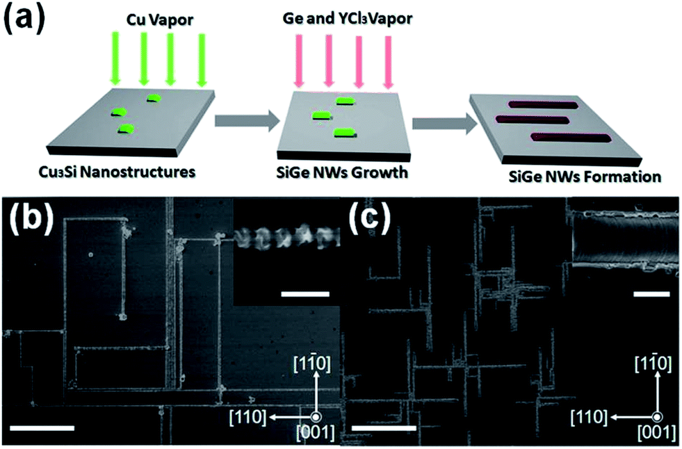 | ||
| Fig. 3 (a) Schematic illustration of the endotaxial SiGe nanowire formation process. SEM images of (b) the aligned SiGe nanowires synthesised at 720 °C on a Si wafer, where the inset shows the enlarged nanostructure, and (c) the same sample after silicate/oxide etching by HF, where the inset shows the enlarged SiGe nanowire surface. Scale bars for (b) and (c) are both 10 μm, 500 nm for the inset of (b), and 200 nm for the inset of (c). “Adapted with permission from ref. 47, copyright 2012, American Chemical Society.” | ||
By choosing suitable substrates, epitaxial approaches have been exploited to control the alignment and crystal orientation of Ge nanowires, where the nanowire growth direction matches the substrate. Molecular beam epitaxy (MBE) has also been used to control the growth direction of Ge nanowires with great success.53,54 MBE is an excellent technique for producing nanowires as it offers ultra-high vacuum conditions (often as high as ∼10−13 bar), precise control over morphology and composition and abrupt interfaces when compound semiconductor nanowires are synthesised. More importantly, MBE offers the ability to study the dynamics of nanowire growth and to control growth at the atomic level more effectively than other techniques, due to the very low deposition rate (often 1 monolayer per second). This extremely low growth rate enables the investigation of the layer-by-layer evolution of nanowires via the VLS mechanism.
Kim et al. and Hawley et al. achieved epitaxial growth of Ge nanowires using CVD approaches.49,84 In particular, taper-free, vertically oriented Ge nanowires were realised by Kim et al. using a Ge buffer layer,48,85 and a two temperature process that was based on the method outlined by Greytak et al.86 (see Fig. 4). Gunji et al. also made use of the two-temperature growth process to grow GeOx nanowires through VLS oxidation.87 The tapering of nanowires was also studied by Hawley et al. where they demonstrated control of the radial growth of Ge nanowires by combining the well-established oxide-assisted-growth (OAG) mechanism88,89 with traditional CVD.84 OAG essentially involves the evaporation and deposition of an oxide vapour to form crystalline nanowires wrapped in an amorphous oxide shell, which prevents radial growth and tapering, thus yielding nanowires with a constant diameter. In contrast to the two-temperature method, the more facile single temperature methods have been used by Simanullang et al. to grow very thin (less than 5 nm) taper-free Ge nanowires.50,90 Vertically aligned epitaxial Ge nanowires have also been achieved using bio-templated Au nanoparticles. Sierra-Sastre et al. used NPs dispersed on S-layer protein templates to produce nanowires with a uniform 〈111〉 growth orientation.91 As the (111) crystal plane has the lowest surface energy of all crystallographic orientations, Ge nanowires grow preferably along a 〈111〉 orientation on Si and Ge substrates. In contrast, nanowires with uniform 〈110〉 orientations have been produced through vertical epitaxial growth on GaAs substrates from Au nanoparticles.92 Additionally, epitaxial growth of Ge nanowires has been achieved using methods such as electron beam evaporation.58 As well as being able to grow aligned epitaxial nanowires with uniform crystallographic orientations, it is also highly desirable to fabricate position-controlled nanowires for device applications. Li et al. used top-down electron beam lithography to pattern Au catalysts particles onto SiO2 substrates, and subsequently employing the CVD of GeH4 to grow Ge nanowires from these substrates.93
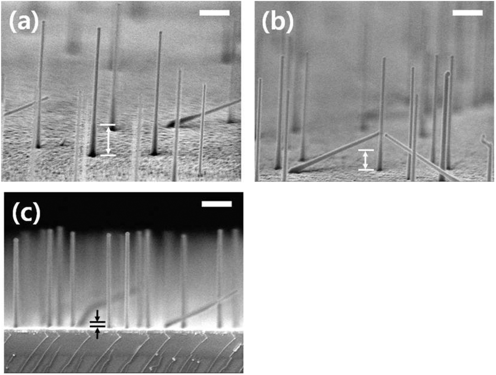 | ||
| Fig. 4 Side-view SEM images of Ge nanowires grown on a GeBSi substrate via a two-temperature process. The growth temperature during the base growth stage was 350 °C, while subsequent nanowire growth was performed at 300 °C for 20 min. The growth time during the base growth stage was: (a) 6 min, (b) 4 min and (c) 2 min. A 50 nm diameter Au colloidal solution was used. The regions marked by arrows in the SEM images are the part of nanowires grown during the base growth stage. Scale bar = 500 nm. “Adapted with permission from ref. 48, copyright 2012, American Chemical Society.” | ||
In comparison to vapour-based methods, solution and SCF-based techniques offer promising alternatives for large-scale synthesis of Ge nanowires. Future methodologies for synthesising Ge nanowires will mostly likely comprise of solution-based techniques, as these afford large scale production of nanowires in a single reaction, as evidenced by Yang et al., who used a liquid injection technique (using several liquid precursors, including diphenylgermane) to scale-up their synthesis of Ge nanowires; producing 0.2 g of nanowires on a Si substrate,51 as shown in Fig. 5. The Ge nanowire product was subsequently scaled up to form a 30 μm thick fabric, from 2.2 g of nanowire product, using a vacuum filtration process. Moreover, Ge nanowire fabrics have also been generated by Smith et al. who investigated the plasticity and strength of the wires.94 The solution-based growth technique offers the possibility of scaling-up product yield for commercial use, giving kilogram quantities of nanowires which can be molded into sheets, fabrics and inks. A SCF is a substance which has been elevated above its critical pressure and temperature. Many of the properties of SCFs vary with density and as such, conducting reactions in SCFs enables the manipulation of the reaction environment through the control of temperature and pressure.95 To this end, the supercritical-fluid–liquid–solid (SFLS) technique has been used to grow Ge nanowires. The SFLS process has also been combined with a templated method to guide the growth of Ge nanowires within anodic alumina membranes via Au catalysed growth.57 These templates offer the capability of pre-aligning nanowires during the growth stage, thus eliminating the requirement for post-alignment. Ge1−xMnx nanowires have also been synthesised using the SFLS technique, where the Mn atoms occupy substitutional sites in the Ge crystal lattice.96 Incorporating Mn into Ge nanowires has been investigated as a means of studying dilute magnetic semiconductors (DMS), as possible building blocks for spintronic devices. Ferromagnetic materials such as Mn and Fe enable the combination of both semiconductor and ferromagnetic functionalities for these devices. The Mn–Ge binary system is of particular interest as many intermetallic compounds formed from these two elements are magnetic. Other examples include the doping of Ge nanowires with Mn by Grossi et al. via the co-evaporation of Ge and Mn powders97 and the syntaxial growth of Ge/Mn-germanide nanowire heterostructures by Lensch-Falk et al. by CVD.98
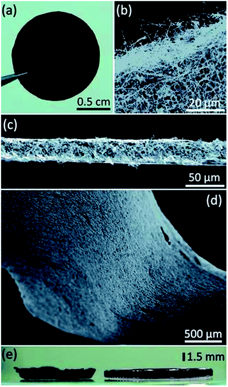 | ||
| Fig. 5 (a) Photograph of Ge nanowire fabric (diameter = 13 mm). SEM images of (b) the edge and (c) the cross-sectional area of a 30 μm thick fabric. (d) SEM image of the surface morphology of the Ge nanowire fabric. (e) Photograph of a 1.5 mm thick Ge nanowire fabric. “Reproduced from ref. 51 with permission from The Royal Society of Chemistry.” | ||
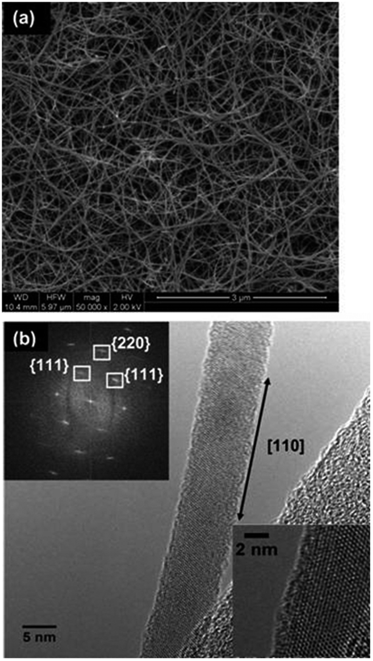 | ||
| Fig. 6 (a) SEM image illustrating the high density 1D Ge nanostructures grown from Ni nanoparticles. The HRTEM image shown in panel (b) represents a highly crystalline nanowire with a 〈110〉 growth direction (inset in panel (b) shows the high crystal quality of the nanowires synthesized). “Adapted with permission from ref. 71, copyright 2011, American Chemical Society.” | ||
2.2. Seedless and self-seeded nanowire growth
Germanium nanowires have also been synthesised without the use of catalytic seeds. Metal particles introduce contaminants into a nanowire system99 which renders their integration into electronic and optoelectronic applications problematic. Lotty et al. used a self-seeded growth method in supercritical toluene to synthesise Ge nanowires, using diphenylgermane as a Ge precursor,69 and proposed a model which accounts for nanoparticle coalescence at the beginning stages of nanowire growth and Ostwald ripening at the later stages. They also used in situ TEM to show that the mean nanowire diameter increased with increasing temperature, as a result of diffusion of Ge particles from the shell to the nanowire core (see Fig. 7). A mechanism for nanowire growth was also proposed. This study extended the work carried out by Hobbs et al.68 on the seedless growth of Ge nanowires from a variety of complex metal/organic precursors and consequently, represents a rather unique method when compared to the more widely reported metal-seeded growth methods. The authors showed that it may be possible in the future to control the diameters of Ge nanowires through the tailoring of precursor molecules. Other seedless methods have also been used to grow Ge nanowires, including a self-induced solid seeding method that makes use of Cu foils.119 Instead of metal nanoparticles acting as growth promoters, the in situ formation of Cu3Ge catalyses the growth of Ge nanowires. Kang et al. also reported the use of Cu3Ge nanocrystals for growing Ge nanowires which eliminated the need for elemental metal seeds. Specifically, the Ge from the source material decomposed into the Cu of the Ni–Cu films which formed Cu3Ge nanocrystals.112 Ge then precipitated out of these nanocrystals, forming Ge nanowires. However, the Ni–Cu bulk alloys produced two types of nanowires that were of non-uniform diameter and crystallinity. The first type were long, thin and typically monocrystalline, while the second category were thick and had extended defects throughout their structure. Unfortunately, both nanowire types were found in abundance from the same reaction, making separation problematic. Cu, a current collector in lithium ion batteries, is an attractive material for growing nanowires. Other copper-germanide derivatives have also been recently used to form Ge nanowires.66 Ge nanowires have also been grown using a seedless, low pressure CVD method on various substrates, including stainless steel and tungsten.120 The Ge nanowires produced were subsequently used as templates for the growth of silicon oxycarbide (Si/O/C) nanotubes. The growth of Ge nanowires on various substrates has also been employment as a means of studying how surface pre-treatments effect growth and have included stainless steel, Fe, Mo, Ta, W, Si and SiO2.121 A Ge buffer layer was used successfully to promote nanowire growth on the Si and SiO2 substrates, a concept which has been reported elsewhere.48,85 A study of Ge nanowires as templates for the growth of other materials was also carried out by Tao et al., in which they were employed as templates for the growth of ZnO nanowires,122 a promising material for photonics due to its wide bandgap of 3.37 eV. Hu et al. also used Ge nanowires as seeds to grow monocrystalline Ge layers on Si.123 The exploitation of Ge nanowires for the subsequent growth of other materials will likely become a prevalent technique in the future, owing to the facile methods that are employed to grow them, in addition to the immense understanding of Ge which has been obtained over the last two decades. Additionally, seedless growth methods are likely to be utilised for the process of growing materials from Ge nanowires as contamination in the Ge nanowire templates and subsequent materials are minimised. Non-metal catalysed template methods have also been used to grow Ge nanowires from ionic liquids, as reported by Al-Salman et al.124 However, the nanowires produced were amorphous with a larger degree of surface roughness and as such, the validity of this technique is questionable. | ||
| Fig. 7 Ge nanowire grown using a self-seeded growth mechanism. In situ TEM heating stage experiments showing the Ge nanowire diameter increasing with temperature. Adapted with permission from ref. 69, copyright 2013, American Chemical Society. | ||
Dailey et al. investigated a “seedless” growth method to synthesise Ge nanowires with a bimodal diameter distribution.125 Here, wires grown from a Au/Si (111) layer displayed narrower diameters than those grown from deposited seeds. Referring to the method as “seedless” is misleading however, as both types of nanowires grow via a modified VLS process, which suggests the presence of a seed particle. Finally, Ge nanowires have been synthesised using a non-catalytic CVD approach in which the temperature was varied to give systematic diameter control.126
2.3. Comparisons of the various growth methods
The choice of growth technique will obviously depend on the availability of specific technical set-ups, the outcome required and the study being carried out. For example, electrical characterisation of Ge nanowires will require an oxide-free surface and the absence of a metal catalyst (if Au is used). Hence, the use of a seedless growth method or an alternative metal catalyst will be preferred. The study of growth dynamics will require isolated, vertically grown nanowires with minute growth rates. Consequently, MBE or cold-wall CVD will be the methods of choice. What follows is a brief discussion of the advantages and disadvantages of the techniques mentioned in the previous sections.CVD is a relatively straight forward technique to employ and involves the germanium precursor being supplied in an oxygen-free vapour form such as germane127 or diphenylgermane.128,129 The advantages and disadvantages of the CVD technique seem to depend on the temperature used. The primary advantage at high temperature growth (above 700 °C) is that the range of catalyst materials that can be used to grow Ge nanowires using the VLS mechanism is greater. Consequently, this allows a greater degree of freedom to alter growth conditions such as temperature and pressure. One possible disadvantage of high temperature CVD is that surface diffusion of atoms (a thermodynamic process) is greater and so Ostwald ripening69 will be significant, resulting in larger seed particles forming at the expense of smaller ones, thus preventing the formation of uniform diameter distributions. Hence, if narrow uniform diameters are desired, then lower temperatures or other methods may be preferred. At low temperatures (less than 500 °C), narrower diameters are possible. Also, doping of the nanowires at lower temperatures is more readily achieved, allowing the more facile tuning of the electrical properties.130 Finally, these temperatures are also more compatible with Si processing temperatures, which is of obvious importance to the semiconductor industry. The solution based methods are similar in principle to CVD, the main difference being that the precursor is supplied as a liquid/solution instead of as a vapour. Therefore, the advantages are comparable to CVD methods with long crystalline quality nanowires being obtained in solution, or as entangled meshes if collected on a substrate. The primary advantage associated with solution methods is the ability to scale up the yield to produce vast quantities of nanowires, as demonstrated by Yang et al.51 The main disadvantage is that controlled growth of vertical isolated nanowires cannot be achieved. The SCF method uses high pressures to grow Ge nanowires, with the precursor delivered within a supercritical-fluid medium, which in turn offers the ability to tune the reaction environment (temperature and pressure).95 The main disadvantage of the SCF technique is the relative complexity of the set-up when compared with CVD.
As mentioned above, the MBE technique makes use of a very high vacuum and ultralow deposition rate. This deposition rate is considered both an advantage and disadvantage with this method. As this incoming flux is so low, it allows the accurate and precise doping of nanowires with defined electrical properties. However, doping of Ge nanowires has been successfully achieved using CVD methods.131 Another advantage is that MBE is often combined with epitaxial growth on various substrates,53,54 offering the ability to produce highly uniform growth orientations. One possible disadvantage of the MBE technique is the small aspect ratio of Ge nanowires which is a result of the limited growth velocity.54
Oxide-assisted growth was briefly mentioned as a method to grow Ge nanowires. This technique was utilized by Lee and co-workers on several occasions to grow Si nanowires.88,132,133 However, it has not been greatly used for the synthesis of Ge. The main disadvantage of the method is that the resulting nanowires possess an oxide shell which would need to be removed before any subsequent electrical characterisation. Additionally, Ge nanowire growth on Si substrates would prove difficult, if not impossible, because the substrate would oxidise rapidly.
The seedless growth methods have the obvious advantage of eliminating the need for a metal catalyst particle. Au is one of the most common catalysts used and because it acts as a recombination center, it is vital that the material is removed or is absent from any nanowire-based electronic devices. Of course, the disadvantage is that the VLS mechanism does not take part in the seedless growth of nanowires. This mechanism is arguably the most commonly used and understood, and the use of seedless methods will require further investigation. Alternative metal catalysts have also been investigated and this potentially offers a more favoured avenue for nanowire growth than seedless methods, as it allows the use of the VLS mechanism while simultaneously preventing contamination from Au. The most likely candidates are Ag and Al which are the other type-A catalysts, as they form simple binary phase diagrams with Ge and are dominated by a single eutectic point.134 As mentioned above, type-B and type-C catalysts have also been investigated. Finally, self-seeded methods often employ films112 or foils119 to seed nanowire growth and these are often composed of materials other than Au. The authors report the formation of a bi-modal diameter distribution for nanowires grown from Ni–Cu bulk alloys,112 which is a disadvantage if uniform diameter distributions are required. Self-seeded growth is a relatively new method and still needs to be investigated further to gain a more complete understanding.
2.4. Nanowire synthesis outlook
The primary challenge facing the bottom-up synthesis of nanowires is a requirement for their post alignment prior to assimilation into devices, as the majority of nanowires are generated as entangled meshes.33,68,71 Whilst several of the approaches outlined above combine growth and alignment into a single process,47,53,54 thus removing the requirement for post-alignment, these techniques are in the minority. The endotaxial method outlined by Li et al. represents a significant step forward in the alignment of Ge nanowires during the growth phase.47 Pre-alignment of a Ge nanowire along (in-plane) and within a substrate is ideal for conventional IC design, which relies on the active channel of the device lying co-planar to the Si wafer substrate. Additionally, methods that make use of randomly oriented nanowires films (without alignment) may be used to create transparent flexible electrodes. This has already been demonstrated for Ag nanowires135 and is more than likely applicable to other nanowire systems.Concerning applications, Ge nanowires are not only considered to be favourable candidates for semiconductor devices, but also as candidates for anodes in lithium-ion batteries. They possess a stable discharge capacity of 1141 mA h g−1 over 20 cycles with a coulombic efficiency of 99%.16 Additionally, Ge nanowires with carbon sheaths have also been investigated for use in batteries.15 Generally, a large reversible capacity, high coulombic efficiency, good rate capability and stable cycle performance make Ge nanowires very suitable for battery related applications. Nanowires, due to their geometry, have certain advantages over thin-film and wafer-based technology in other applications such as solar cells136 and photodetectors.137,138 These advantages include reduced reflection, facile band gap tuning and extreme light trapping. Benefits such as these obtained from utilising nanowires in photovoltaic devices are expected to reduce the quality and quantity of material required to reach already established limits, which reduces cost. Specifically, Ge nanowires have been used in photodetectors, with Kim et al. reporting a diameter dependent photoconduction gain.137 This further demonstrates the need to control nanowire dimensions using well understood growth methods such as the VLS mechanism. Cao et al. demonstrate that Ge nanowires are ideally suited to improve and spectrally tune light absorption in these devices.138 As the focus of this article is on the growth of Ge nanowires, a detailed discussion on applications is beyond the scope of the work. A more thorough account on the applications of Ge nanowires can be found elsewhere.8,12 Finally, the ability to realise these applications and the effectiveness of Ge nanowires as a nanoscale component will depend on the ability to control its growth. This can only be achieved through the continued investigation of the synthetic methods outlined above.
3. Kinetics and thermodynamics of Ge nanowire growth
3.1. The Au/Ge system
Successful implementation of Ge-based technology will require an in-depth understanding of the solid-state and molten interactions in metal–germanium systems. The Au/Ge system in particular is important for the growth of Ge nanowires, as Au forms a deep low-temperature eutectic with Ge and has been employed successfully in semiconductor nanowire growth for many years. The behaviour of this system is predicted by the Au/Ge bulk phase diagram and can be used to trace the progression of an Au/Ge binary alloy from a solid Au film to Ge nanowire growth, as the concentration of the Ge component in the two-phase system increases. However, care has to be taken as deviations from the bulk phase diagrams occur in nanoscale systems, such as the Au/Ge alloy particles used to seed nanowire growth.139–142 Specifically, the eutectic temperature and eutectic composition are reduced in nanoscale systems due to capillary effects, which are often represented by the Gibbs–Thomson equation.143 Sutter et al. have investigated the nanoscale phase diagram of the Au/Ge system and used it to predict the temperature-dependent equilibrium composition of the alloy drops at the tips of Ge nanowires.141,142 Surprisingly, the work carried out by Kim et al. on the Au–Si system yielded results that were contrary to those obtained by Sutter et al.144 Kim et al. found that the Au–Si phase diagram had no observable size dependence as there was no change in supersaturation with particle volume. The melting behaviour of a Au/Ge bi-layer was also investigated by Kryshtal et al. who observed that liquid-phase formation at the eutectic temperature only occurred if the Au film thickness was above a critical value.145The difference between the bulk and nanoscale phase diagrams of the Au/Ge alloy system were also investigated by Chueh et al. The difference was highlighted by varying the Au concentration in the wires and then utilising an annealing/cooling step to induce phase separation of the Au and the Ge.146 Ge will phase separate from Au upon cooling due to the differences in their surface energies147 and depending on the amount of Au present, a variety of structures ranging from pyramid shaped nanoislands to uniform core–shell structures can be formed, as shown in Fig. 8. The formation of various nanostructures (which included islands, periodic nanodisks and core–shell structures) was explained by the phase diagram,142 with the authors controlling the atomic percentage of Au and thermal annealing above the eutectic temperature.
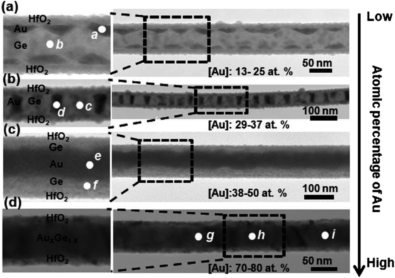 | ||
| Fig. 8 TEM images of the enabled Au/Ge nanostructures after thermal annealing at 450 °C for nanowires with: (a) 13–25, (b) 29–37, (c) 38–5, and (d) 70–80 atom% Au. Adapted with permission from ref. 146, copyright 2010, American Chemical Society. | ||
The Au/Ge system has been investigated for other applications such as alternatives to Pb containing solders148–150 and as such, its structure has the been the focus of much examination.151–154 Findings have contradicted the common understanding that Au/Ge does not form germanide compounds. For example, Tasci et al. identified the formation of a Au5Ge2 compound in which the Ge was coordinated by 6 Au atoms154 while Takeda et al. inferred from reverse Monte Carlo simulations that Ge atoms locate at the substitutional positions of the Au atoms.152 Comparatively, neutron diffraction has also been used to study the structure of a Au0.72Ge0.28 eutectic system,155 while the electronic band structure of Au/Ge was investigated using angle-resolved photoemission and density functional theory calculations.156 Additionally, Au nanocatalysts on the tips of Ge nanowires mostly adopt a face-centered-cubic structure, but a minority (about 10%) crystallise in a hexagonal close-packed structure upon solidification.157
Studies into the Au–Ge system as part of a ternary alloy have also been conducted. One possible advantage of using a ternary alloy system instead of a binary system is that it may allow the incorporation of dopants into the interior of a Ge nanowire through the alloy droplet60 and potentially avoids the difficulties linked with the surface deposition of dopants. Ternary systems which have been investigated and modelled include the Au–Ge–Ni,158 Au–Ag–Ge,159 Au–Ge–Sb160 and Au–Ge–Sn161 systems.
3.2. Thermodynamic considerations
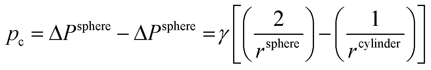
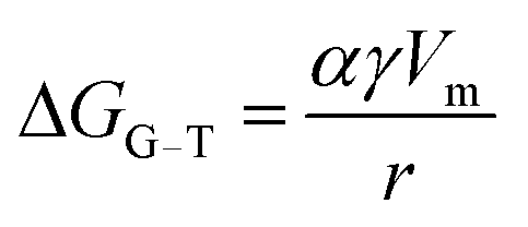
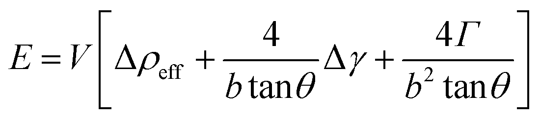
A prerequisite for the integration of nanowires into devices is to be able to understand the kinetic and thermodynamic principles which dictate their controlled synthesis.162–165 Thermodynamic aspects of Si nanowire growth have been reported elsewhere,134,144,166–171 due to the importance of Si in current CMOS based devices. In this section, the thermodynamic and kinetic aspects of Ge nanowire growth will be detailed.One method often utilised to study the dynamics of nanowire growth is in situ transmission electron microscopy (TEM). In particular, video-rate lattice-resolved environmental TEM172,173 allows the introduction of a gaseous precursor into the microscopy cell, enabling the observation of nanowire growth in real time. As in situ TEM allows the examination of nanoscale systems as they undergo physical transformation, e.g. upon heating for example, insights into the liquid–solid interface behaviour between a metal tip and a semiconductor nanowire, phase nucleation and the mechanisms controlling nucleation and nanowire growth can be obtained.174–176 For example, Holmberg et al. used in situ TEM to carry out temperature-dependent studies on Ge nanowires encapsulated within amorphous carbon shells,143 as shown in Fig. 9. They found that as the temperature increased, the liquid–solid interface expanded into the wire while Ge re-crystallised in the spherical tip. This expansion was attributed to a capillary effect, as shown in eqn (1), directly resulting from the presence of the carbon shell:
 | (1) |
 | (2) |
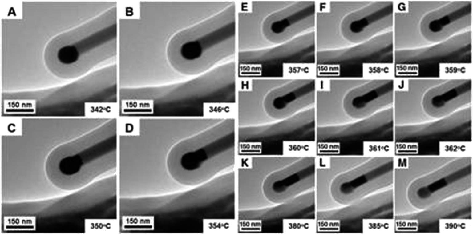 | ||
| Fig. 9 TEM images of a Au seed particle melted at 346 °C which migrates into the stem of the nanowire with increasing temperature. Ge recrystallised in the spherical end as the Au/Ge melt shifts into the neck of the nanowire. “From ref. 143, reprinted with permission from AAAS.” | ||
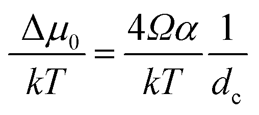
Gamalski et al. used in situ TEM to study the metastability of Au/Ge catalysts below the eutectic temperature and found that both solid and liquid metastable phases are possible.172,173 The phase of the catalyst is significant in determining how rapidly the chemical potential of the system can be increased to overcome the kinetic barrier for nucleation; thus determining the rate of interfacial ledge formation.116 Gamalski et al.173 suggested that the liquid metastable phase may be a result of a high nucleation barrier to forming diamond-cubic Ge, while the Au/Ge liquid phase is thermodynamically and kinetically accessible according to eqn (3):173
 | (3) |
 | ||
| Fig. 10 (a) to (e) Sequence of TEM images of a Ge nanowire close to the nanowire tip during in situ annealing experiments at different temperatures; between room temperature and 575 °C. (a) Au–Ge alloy crystalline nanoparticle adjacent to the Ge nanowire before surface melting starts, (b) to (e) exchange of material across the Ge nanowire–liquid drop interface after melting of the alloy Au–Ge nanoparticle and (f) Au–Ge binary alloy phase diagram. “Adapted with permission from ref. 141, copyright 2010, American Chemical Society.” | ||
One of the most significant contributions to the study of droplet–nanowire interface behaviour in Ge nanowires78 was the establishment of a nanoscale phase diagram and its comparison to the bulk counterpart by Sutter et al.140–142 Estimation of equilibrium concentration along the Ge-liquidus was achieved using in situ TEM and described how the droplet adjusted its composition upon heating or cooling to achieve an equilibrium Ge concentration according to the adjusted nanoscale phase diagram. Exchanging Ge atoms with the nanowire causes an expansion or contraction of the droplet size depending on whether it is heated or cooled. This exchange also causes a change in the faceting of the droplet–nanowire interface during the particle expansion/contraction. The Ge composition, which was used to establish the nanoscale phase diagram was determined using eqn (4):
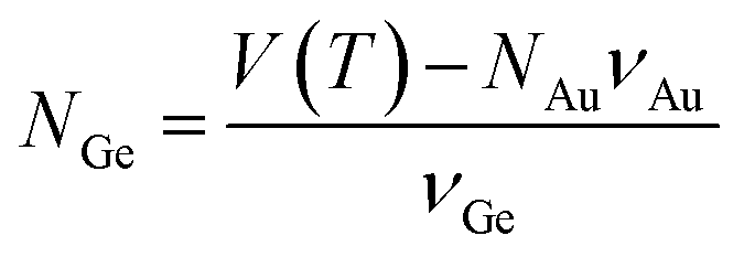 | (4) |
 | (5) |
Thermodynamic concepts have also been used to account for the seedless growth of Ge nanowires, using MBE on Si (001) substrates. A thermodynamic model was proposed (eqn (6)) which explained that the driving force for Ge nanowire formation is the reduction of surface energy, rather than strain relaxation:183
 | (6) |
3.3. Kinetic considerations
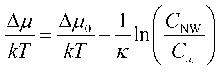
The kinetics of Si nanowhisker growth was first investigated by Givargizov in 1975 (ref. 177) and involved an investigation of the supersaturation as a function of nanowhisker/seed particle diameter as governed by the Gibbs–Thompson effect (eqn (7)). Other kinetic parameters, such as the relationship between the nanowhisker growth rate and the supersaturation (eqn (8)) and the critical diameter, i.e. the lower limit of the thermodynamically attainable nanowire diameter in a nucleation mediated growth (eqn (9)). These expressions are given below: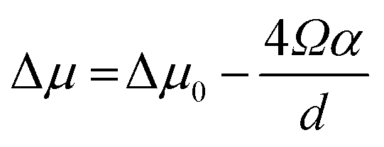 | (7) |
| V ∼ (Δμ/kT)n | (8) |
 | (9) |
 | (10) |
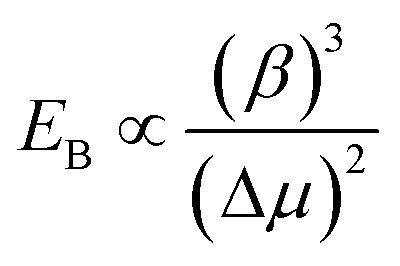
In addition to the work carried out by Gamalski et al. on the metastability of Au/Ge catalyst particles,172,173 this group have also investigated nanowire nucleation kinetics at the triple phase boundary (TPB), in a Au/Ge binary system for VLS-based nanowire growth75 (see Fig. 11). A cyclic supersaturation model, whereby a new Ge bi-layer forms at the TPB upon overcoming an activation energy barrier for nucleation was inferred as shown by eqn (11):
| ΔGB = α2/(4Δμ) | (11) |
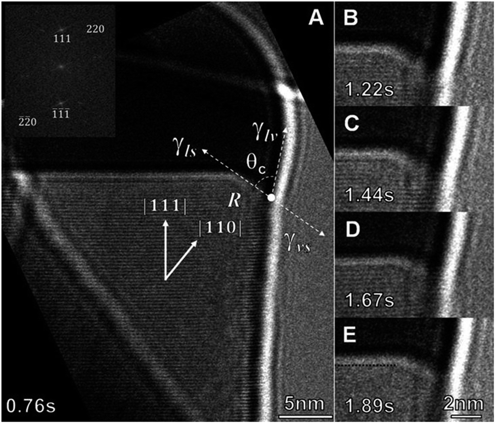 | ||
| Fig. 11 Bright field ETEM image sequence of the catalyst interface around the TPB of a growing Ge nanowire at ≈310 °C in Ge2H6. In (A) the atomically rough surface is denoted by R, the wetting angle by θc, and γlv, γls, and γvs are the surface energy differences between the liquid–vapour, liquid–solid, and vapour–solid surfaces, respectively. The inset shows a selected area fast fourier transform of the Ge nanowire. In (E) the original (111) solid–liquid interface is traced with a dotted black line to highlight the advancement of the growth interface. “Adapted with permission from ref. 75, copyright 2011, American Chemical Society.” | ||
The size of this barrier determines the rate of nucleation and thus the overall nanowire growth rate. In a cyclic process, the wetting angle of the catalyst increases as Ge precipitates at the rough TPB region, thus continuously increasing supersaturation during the cycle. Continued rising of the supersaturation results in a fall of the kinetic energy barrier for Ge bi-layer formation and step nucleation at the TPB. Step flow lowers the supersaturation and causes the dissolution of the Ge in the TPB region completing a growth cycle. Nanowire nucleation and growth has also been shown to depend on parameters such as substrate temperature, Ge deposition rate and surface diffusion length.185
Kim et al. have studied the low-temperature catalytic growth of Ge nanowires and identified three pathways by which growth can proceed, depending on the temperature employed.186 They rationalised that the pathways arise due to kinetic competition between the imposed timescale for Ge addition (τAu) and the inherent time scale for Ge nucleation in the Au and Au/Ge system (τGe), where the latter timescale is described by eqn (12):
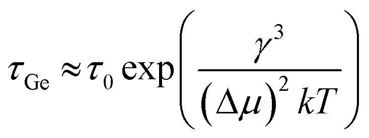 | (12) |
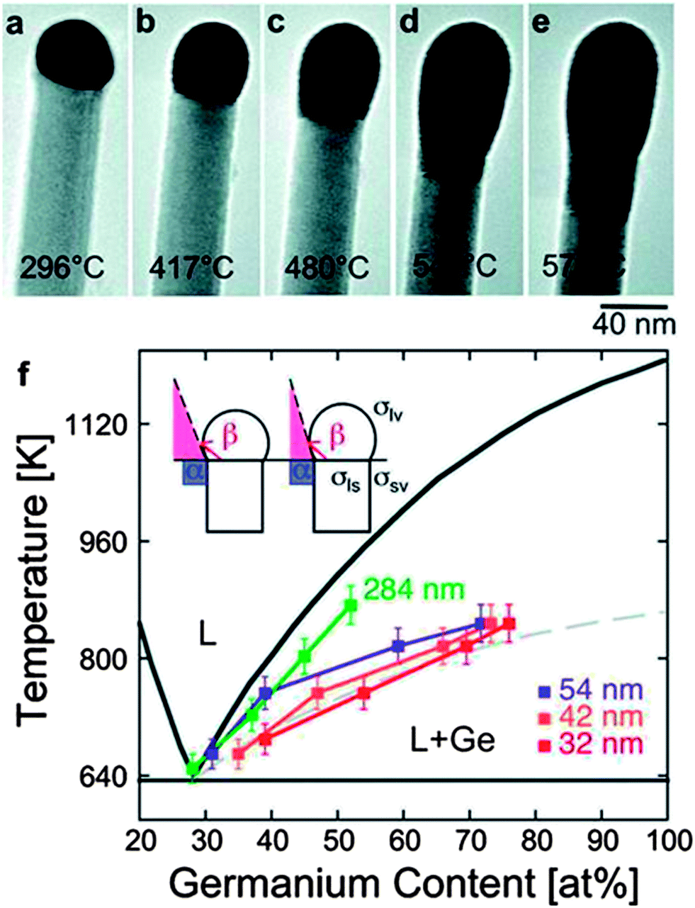
The differences in the growth kinetics between Ge and Si nanowires have been studied by Artoni et al.,168 who observed that the two material systems grow in different temperature and time regimes, even though Si and Ge share similar properties, crystal structures and phase diagrams. Ge nanowire growth was limited by the eutectic temperature only (a thermodynamic constraint), while Si nanowire growth was limited kinetically due to the low activation energy of surface diffusion of Si atoms. Additionally, the incubation times were much higher for Si nanowire growth. Also, a considerable difference (approximately 60%) in critical diameter was observed between Ge and Si nanowire growth due to the difference in surface energies, atomic volumes, and supersaturation.187
While the VLS mechanism has been studied in detail for Ge nanowire growth, the VSS mechanism remains relatively unexplored for most material systems, including Ge. A limited number of reports have been presented, highlighting diffusion limited models for VSS nanowire growth.188,189 Despite the fact that these were based on III–V systems, the diffusion-limited approach (as opposed to supersaturation-limited) illustrated in these investigations should be applicable to Ge provided that certain assumptions are valid.188 These assumptions include a hemispherical particle, a large interwire separation, negligible diffusion within the seed and steady-state adatom diffusion on the substrate and nanowire sides. While there have not been any reports detailing the VSS mechanism in Ge nanowires to date, it is likely that the VSS growth model will become more understood in the future, due to the increasing popularity of sub-eutectic nanowire growth techniques.
4. Morphology control in Ge nanowires
Investigations into understanding and controlling nanowire morphology, e.g. length, diameter, orientation, has largely been achieved using in situ TEM approaches, due to ability to observe real-time morphological changes in the structure of nanowires.176,186,190 As discussed above, morphological changes can be induced in Ge nanowire surfaces through annealing and adjusting the Au composition.146 Changes in the morphology of Ge nanowires can also be achieved by varying the catalyst material used as the growth seed.56 Schwarz et al. proposed a simple model to explain morphological changes in nanowires grown via the VLS mechanism and postulated that three elementary processes are responsible for a variety of growth behaviours:163 facet dynamics, droplet statics and the introduction of new facets. These processes were responsible for changes in VLS grown nanowire morphologies and resulted in straight wires, kinked nanowires and nanowires which crawl along the surface. Their model placed particular importance on the capillary force exerted by the liquid at the TPB; a concept which has been discussed more recently in terms of nanowire morphology by Gamalski et al.75Generally, nanowire morphology can be discussed in terms of kinks, defects, twins and overall crystallinity. Controllable crystallinity of Ge nanostructures was achieved by Petkov et al. through the use of channelled alumina surfaces.57 The same group also studied the defect formation in Ge more recently through the use of Ag and AuxAg1−x alloy seeds70,114 and observed that defects could be transferred into Ge nanowires from the seed particles via a supercritical-fluid–solid–solid (SFSS) process using both Ag and AuxAg1−x alloy seeds. The choice of seed was based on meeting several criteria including: low twin formation energy, the presence of a solid-phase seeding regime and similar structure and lattice constants between the particle and the nanowire. The transfer of crystallographic information from a seed particle to a nanowire opens up the possibility of engineering the structure of Ge nanowires and enabling the tuning of band structure via strain modulation. Kinking and defects in Ge nanowires were also investigated by Geaney et al. who used a high boiling point (HBS) method to vary the synthesis temperature to produce straight nanowires consisting of stacking faults (longitudinal and transverse), kinked nanowires and tortuous nanowires.191 While kinked nanowires may have limited applications outside of three-dimensional electronics,192 the study of such architectures provides an understanding of how kinks are formed, thus enabling future generations of researchers to more accurately synthesise straight wires of uniform structural integrity.
4.1. Diameter and length control
The control of nanowire diameters and lengths is considered to be of paramount importance due to the dimensional dependency of nanoscale properties. Kim et al. have investigated the control of nanowire diameters via a two-temperature process.48 They suggested that the use of low growth temperatures can prevent tapering of Ge nanowires, as diffusing adatoms are less likely to be assimilated onto the nanowire sidewalls, ensuring uniform nanowire diameters which can be seeded by Au particles of varying sizes. Seedless growth methods have been effectively used to grow Ge nanowires with tunable diameters in the past few years, by varying the partial pressures and temperatures employed.126 Ge nanowire diameters have been controlled to produce ultra-thin nanowires in the absence of conventional metal seeds, with reports quoting diameters below 10 nm.68,69 Both reports used complex organometallic Ge precursors to grow the nanowires, which consist of an amorphous shell around the Ge core, that helps passivate the nanowire surfaces and maintains a uniform diameter. The same group also used solid phase seeding (via a SFSS approach) of Ge nanowires using size-selective Ni seeds which enabled wires to be synthesised with mean diameters of 9.3 and 14.2 nm respectively.71 Controlling the size of the original metal seed was vital to achieving governable nanowire diameters. Solid phase catalytic seeds with high melting points, Ni, Cu, Fe etc., offer controlled inter-particle diffusion and precise control over radial dimension of nanowires.71,111 However, during nanowire growth these seeds form germanides which increase the volume of the seeds by up to 300%, with an increase in the lower limit of attainable nanowire diameter. Biswas et al. have looked into this seed expansion problem and have used AgxAu1−x growth promoters, which do not go through any germination, to synthesise diameter controlled nanowires in the sub-10 nm regime.70 Diameter controlled seed particles were also utilised by Wen et al. to regulate the diameter of Ge nanowires grown from Au nanoparticles.67 The diameters of the nanowires (40 and 80 nm) were found to exactly match the diameter of the nanoparticles.The use of amorphous sheaths, as mentioned previously,143,146 have been used successfully to control the diameters of Ge nanowires. The technique is analogous to controlling nanowire diameter via template pores such as anodic aluminium oxide,193 as the sheath can be likened to a pore from which the nanowire grows. Materials used for sheaths include carbon,194 oxides84 and multi-walled carbon nanotubes.82 The use of a carbon sheath appears to be particularly effective because one-dimensional carbon materials can be grown using the VLS process with the same metal catalysts used for Ge.195,196 The carbon sheath is also immiscible with Ge and is formed simultaneously with the wire during VLS growth. The sheath was found to completely block vapour deposition on the nanowire sidewalls, preventing tapering and thus giving highly uniform diameters, as shown in Fig. 12.194
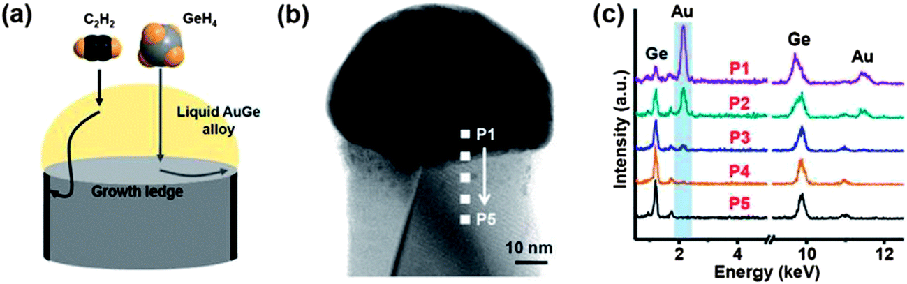 | ||
| Fig. 12 (a) Schematic for carbon sheath formation during the Ge nanowire growth process, (b) bright-field STEM image of a single Ge nanowire with a carbon sheath and (c) EDS analysis of the corresponding nanowire from the positions P1 to P5. This data shows that Au diffusion does not occur below the carbon sheath. “Adapted with permission from ref. 194, copyright 2012, American Chemical Society.” | ||
Length is also a factor which can be affected by the temperature of the growth process, as was shown by Pecora et al. when they investigated the epitaxial growth of Ge nanowires of various orientations.58 They reported that the length of the wires increased as the temperature increased from 380 to 520 °C and that the lengths varied at a specific temperature depending on the growth orientation. Nanowire lengths can usually be altered by varying the growth time of the reaction and generally there is a linear dependence present.197 In other words, the time frame over which the precursor is injected into the system in a typical CVD set-up determines the length of the resulting nanowires and is logical because when the injection stops, there is no longer any incorporation of the semiconductor material into the nanowire and therefore growth discontinues. Other methods of tuning the length of nanowires may involve manipulating the kinetics at the liquid–solid interface via the supersaturation of the metal seed particle.70,198 Dubrovskii et al. have demonstrated the narrowing of the length distribution of Ge nanowires and also presented a theoretical model to explain the behaviour.197 An interesting conclusion from this report was that as the growth time was decreased from 70 to 15 minutes, the diameter dependence of the length changed. At higher growth times, the length increased with diameter which can be explained by the Gibbs–Thomson effect. However, at lower growth times, nanowire lengths decreased with increasing diameter, which suggested the presence of a diffusion-induced growth regime.
4.2. Growth orientation
The control of nanowire growth orientation is highly desirable, as the electronic and optical properties of the nanowire are often orientation dependent, and has been a topic of much investigation in recent years.199 The orientation of nanowires has been shown to be diameter dependent200 and additionally, certain nanowire facets are more energetically favourable than others, thus an understanding of growth orientation and faceting is vital for growth engineering. One common method of controlling the orientation of Ge nanowires is through epitaxial growth from substrates such as GaAs (110),92 Si(111)201,202 and Ge (111).202 The underlying substrate orientation guides the crystallographic growth direction of the nanowires due to lattice matching. Ge nanowires have been observed to grow principally along the 〈110〉 direction from GaAs substrates whereas Si and Ge substrates commonly produce nanowires with a 〈111〉 growth direction. However, Ge(111) substrates have also been reported to yielding Ge nanowires with a predominately 〈110〉 orientation.202Ge nanowires with a 〈110〉 growth direction have also been synthesised by Quitoriano et al.203 using SOITEC (001) oriented silicon-on-insulator substrates. Nanowires could be reproducibly grown along the 〈110〉 direction and the authors compared this to unguided growth on a regular substrate in which the nanowires mostly adopted a 〈111〉 orientation. As mentioned previously, solid phase seeding of Ge nanowires, via a VSS mechanism using Ni nanoparticles, could be used to control nanowire diameters.71 A similar method was also used by Thombare et al.204 to highlight that narrow diameter Ge nanowires (below 25 nm) adopted a predominantly 〈110〉 orientation and were free from kinks and defects, while larger diameter wires (above 25 nm) had a prevalent 〈111〉 orientation, with a high density of defects and kinks (Fig. 13). This orientation dependence on diameter has previously been reported by Schmidt et al.200 who also reported a transition diameter of around 25 nm. A prevailing 〈112〉 growth direction was observed for axially twinned Ge nanowires205 where twin boundaries propagate along the length of the nanowires.70,114 Supersaturation controlled manipulation of the liquid–solid interface kinetics have previously been used to control orientations for GaAs nanowires,198 suggesting the method would also be applicable to Ge nanowire growth.
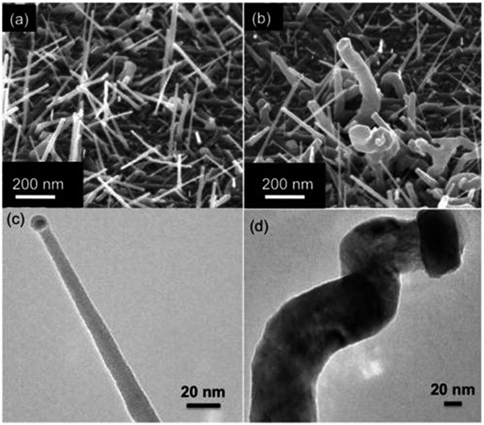 | ||
| Fig. 13 (a) and (b) Show SEM images of different regions on the same VSS-grown sample (a) shows Ge nanowires of <25 diameter with a straight morphology while (b) shows larger diameter nanowires with a tortuous morphology resulting from continuous kinking during growth. TEM Images (c) and (d) show smaller and larger diameter nanowires with straight and kinked morphologies, respectively. “Reprinted with permission from ref. 204. Copyright 2012, AIP Publishing LLC.” | ||
4.3. Heterostructures
Research into heterostructured nanowires has focused on forming compositionally abrupt interfaces between wire segments, which is vital for reproducible and predictable behaviour across nanowire junctions. Wen et al.118 have investigated the use of Al–Au alloy catalyst particles to seed the growth of Si–Ge nanowires and form abrupt heterojunctions (see Fig. 14). They confirmed the ability to modulate the junction on the nanoscale via a VSS mechanism and obtain an interfacial abruptness of below 1 nm. The same group also reported the use of Ag–Au catalysts to control the heterojunction in Si–Ge nanowires206 and the application of regular Au–Ge catalysts to form heterostructured nanowires of group IV and III–V materials.207 The abruptness of the heterojunction using the Ag–Au catalysts was approximately 1.3 nm and so offers similar benefits as the Al–Au alloy. Both the use of Ag–Au and Au–Al catalysts employ a VSS type growth mechanism (Ag–Au catalysts can also seed wires via a VLS mechanism, depending on which alloy composition is present) and have the advantage of very low solid solubility of Si and Ge in the seed metals. One of the primary disadvantages of the VSS mechanism is that it yields a lower nanowire growth rate compared to the VLS mechanism. An ideal scenario would be to take advantage of the standard VLS mechanism, to ensure a high growth rate, in combination with a VSS-type process to yield compositionally abrupt interfaces at the same time. Interestingly, Geaney et al. have reported the VLS growth of Si–Ge nanowires with an interface abruptness of 1–2 atomic planes, confirmed by atomic-resolution STEM-EELS analysis.208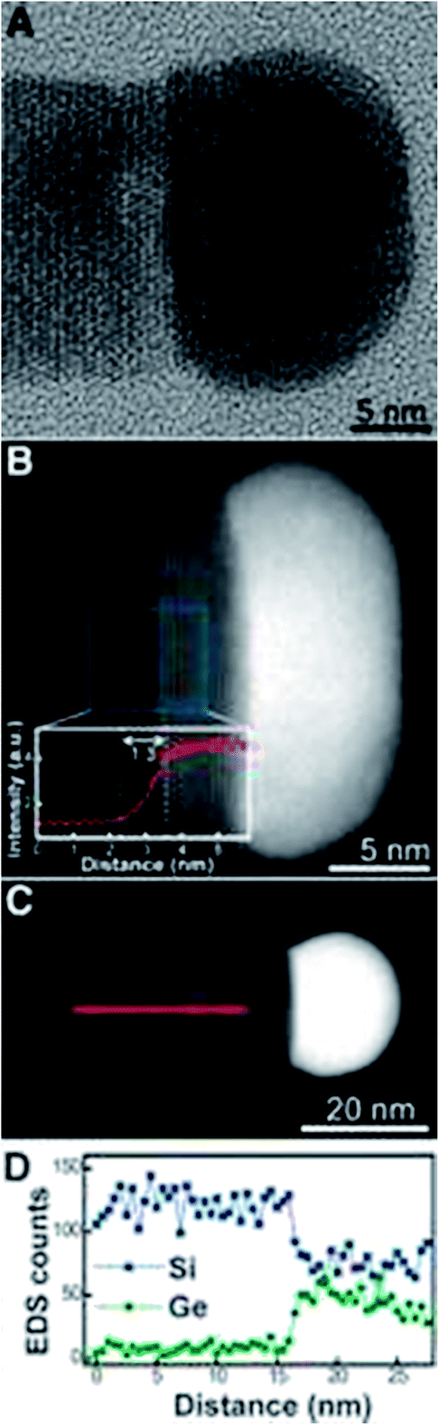 | ||
| Fig. 14 TEM and STEM analysis of a Si–Ge heterojunction nanowire. (A) High-resolution TEM image of a Si–Ge heterojunction nanowire. (B) HAADF-STEM image of a wire (diameter 17 nm). The inset shows the intensity profile across the interface, averaged over a 5 nm strip along the midpoint of the wire. The width of the interface is 1.3 nm. (C) HAADFSTEM image of a Si/Si1−xGex nanowire (diameter 21 nm). (D) EDS line profile of Si and Ge through the Si/Si1−xGex junction, as indicated in (C), showing a sharp transition (less than 2 nm) from Si to SiGe. The composition of the Si1−xGex alloy segment is estimated to be Si0.7Ge0.3. “From ref. 118, reprinted with permission from AAAS.” | ||
In contrast to the highly abrupt interfaces reported above, Clark et al.209 identified diffuse interfaces and noticeable broadening with increasing nanowire diameter. Interfacial broadening is normally due to the “reservoir” effect whereby a significant amount of the semiconductor material remains in the seed particle after the source of precursor has ceased, resulting in a compositional gradient at the junction between the two materials in question (in this case, Si and Si1−xGex). The broadening presents one of the fundamental challenges to the fabrication of abrupt heterojunctions. Dayeh et al.210 report 100% compositional modulation in Ge–Si nanowire heterostructures through Au catalysts via the VLS mechanism. Interfacial abruptness was not the focus of the report however, and this effect was not investigated in detail. Instead, the group studied defects in the stacking sequence and how they affected the TPB behaviour and nanowire morphology. Several reports have been published describing the interfacial abruptness from a theoretical/modelling point of view,211,212 and this may be the most promising method of gaining greater insight into the formation of sharp interfaces.
Other interesting Ge nanowire heterostructures which have been investigated include Ge nanowire–GeSiOx nanotubes,213 radial core–shell heterostructures of Ge–SiOx83 and Ge–γAuGe nanowires.140 In particular, the last report is of interest due to the presence of both stable and metastable phases in the same nanowire. The authors present a method to grow Ge nanowires with both stable and metastable phases via the VLS mechanism. They heat the wires in situ and observe how the liquid–solid interface expands into the nanowire due to the uptake of Ge into the seed. Interestingly, the interface does not recede upon cooling, but crystallises into metastable γAuGe with the top of the seed remaining in the liquid phase. The interface between the Ge and γAuGe appears to be about 1 nm in length which is comparable to reports already mentioned.118,206
5. Conclusion and outlook
The vast body of research that has accumulated over the past decade has made the semiconducting nanowire a strong candidate for future CMOS based devices.214 The shift in the structure of the channel material in MOSFET devices from a planar configuration to architectures with reduced dimensionalities has necessitated the development of one-dimensional structures. As Ge shares many properties with Si, the material is sure to be at the forefront of any future developments. The wealth of synthetic methods available, the improved transport properties over Si and the ability to better control the morphology of Ge nanowires will ensure its placement as one of the leading materials for nanoscale development. Lieber et al. conclude that the three key ingredients to the nanowire system are the single-crystalline nature of the material, quantum confinement effects at narrow diameters and the ability to tailor the morphology of the nanowire itself.215 The growth techniques employed along with an understanding of the growth kinetics and thermodynamics of the Au/Ge system are crucial to producing monocrystalline Ge and controlling the nanowire morphology, which in turn, is necessary to synthesise nanowires with highly uniform, narrow diameters so that these confinement effects can be taken advantage of. Consequently, this article has reviewed these aspects which are most critical to the advancement of Ge nanowire growth. The most common synthetic methods have been detailed as well as the most recent studies in dynamics and morphology control. As a result of the fundamental breakthroughs that have been achieved in these three main areas of Ge nanowire research over the last decade, the realisation of Ge nanowire based applications, such as lithium-ion batteries,14–16 field effect transistors (FETs),17,18 memory applications,19–21 photovoltaics22,23 and nanoelectromechanical systems (NEMS)24,25 draws ever closer.Semiconducting nanowires can now be synthesised in large quantities using gas and solution based techniques, as evidenced by reports such as that by Yang et al.51 which is promising for industry scale production. One key issue to address is the combination of top-down versus bottom up paradigms to produce Ge nanowires in large quantities and in controlled orientations and placements.43 One of the most noteworthy publications that was mentioned in this article was the endotaxial growth of Ge via the VLS mechanism,47 which describes the growth of nanowires along a substrate, which results in aligned nanowires. Consequently, the combination of the scaling up methods developed by Yang et al.51 and endotaxial growth along substrates may enable the simultaneous alignment of commercial scale quantities of Ge nanowires in the future. Li et al.47 report that the primary criteria to be satisfied include the dissolving of the catalyst into the substrate and the prevention of the catalyst from moving along the substrate. The use of substrates of sufficient size will also be necessary if large quantities are to be produced, but despite these limitations, this method holds substantial promise as a viable means to produce aligned Ge nanowires for commercial scale applications. Conversely, the ability to manufacture contacts and devices based on random nanowire networks135 may provide an interesting alternative to alignment, as this would eliminate the need to align the nanowires before integration.
Even as isolated architectures, Ge nanowires are ideal platforms for the investigation of material properties on the nanoscale. Accurate comparisons between bulk and nanoscale materials can be achieved through the investigation of nanowires, both via in situ as they grow and ex situ after growth has finished. Furthermore, additional aspects such as defect density, recombination processes and interface behaviour at heterojunctions need to be completely understood via isolated nanowire studies in order for these promising materials to be utilised to their full potential.8
Acknowledgements
We acknowledge financial support from the Irish Research Council for Science Engineering and Technology (IRCSET) and Science Foundation Ireland (Grants: 09/SIRG/I1621, 06/IN.1/I106, 08/CE/I1432 and 09/IN.1/I2602). This research was also enabled by the Higher Education Authority Program for Research in Third Level Institutions (2007–2011) via the INSPIRE programme.References
- Y. Cui and C. Lieber, Science, 2001, 291, 851 CrossRef CAS PubMed.
- V. Dubrovskii, G. Cirlin and V. Ustinov, Semiconductors, 2009, 43, 1539 CrossRef CAS.
- K. Peng, Y. Xu, Y. Wu, Y. Yan, S. Lee and J. Zhu, Small, 2005, 1, 1062 CrossRef CAS PubMed.
- X. Duan, Y. Huang, Y. Cui, J. Wang and C. Lieber, Nature, 2001, 409, 66 CrossRef CAS PubMed.
- J. Lee, S. Mahendra and P. J. J. Alvarez, ACS Nano, 2010, 4, 3580 CrossRef CAS PubMed.
- A. I. Hochbaum and P. Yang, Chem. Rev., 2010, 110, 527 CrossRef CAS PubMed.
- Y. Huang and C. Lieber, Pure Appl. Chem., 2004, 76, 2051 CrossRef CAS.
- S. Barth, F. Hernandez-Ramirez, J. D. Holmes and A. Romano-Rodriguez, Prog. Mater. Sci., 2010, 55, 563 CrossRef CAS PubMed.
- R. Yan, D. Gargas and P. Yang, Nat. Photonics, 2009, 3, 569 CrossRef CAS.
- R. R. Schaller, IEEE Spectrum, 1997, 34, 52 CrossRef.
- P. Nguyen, H. Ng and M. Meyyappan, Adv. Mater., 2005, 17, 549 CrossRef CAS.
- L. Z. Pei and Z. Y. Cai, Recent Pat. Nanotechnol., 2012, 6, 44 CrossRef CAS.
- X. Wu, J. S. Kulkarni, G. Collins, N. Petkov, D. Almecija, J. J. Boland, D. Erts and J. D. Holmes, Chem. Mater., 2008, 20, 5954 CrossRef CAS.
- A. M. Chockla, K. C. Klavetter, C. B. Mullins and B. A. Korgel, ACS Appl. Mater. Interfaces, 2012, 4, 4658 CAS.
- M. H. Seo, M. Park, K. T. Lee, K. Kim, J. Kim and J. Cho, Energy Environ. Sci., 2011, 4, 425 CAS.
- C. K. Chan, X. F. Zhang and Y. Cui, Nano Lett., 2008, 8, 307 CrossRef CAS PubMed.
- S. T. Le, P. Jannaty, X. Luo, A. Zaslavsky, D. E. Perea, S. A. Dayeh and S. T. Picraux, Nano Lett., 2012, 12, 5850 CrossRef CAS PubMed.
- T. Burchhart, A. Lugstein, Y. J. Hyun, G. Hochleitner and E. Bertagnolli, Nano Lett., 2009, 9, 3739 CrossRef CAS PubMed.
- X. Sun, B. Yu, G. Ng, M. Meyyappan, S. Ju and D. B. Janes, IEEE Trans. Electron Devices, 2008, 55, 3131 CrossRef CAS.
- S. B. Kim, Y. Zhang, J. P. McVittie, H. Jagannathan, Y. Nishi and H. S. P. Wong, IEEE Trans. Electron Devices, 2008, 55, 2307 CrossRef CAS.
- Y. Jung, S. W. Nam and R. Agarwal, Nano Lett., 2011, 11, 1364 CrossRef CAS PubMed.
- E. Garfunkel, D. Mastrogiovanni, L. Klein, A. Wan and A. Du Pasquier, Abstr. Pap. Am. Chem. Soc., 2008, 236, 454 Search PubMed.
- C. Pan, Z. Luo, C. Xu, J. Luo, R. Liang, G. Zhu, W. Wu, W. Guo, X. Yan, J. Xu, Z. L. Wang and J. Zhu, ACS Nano, 2011, 5, 6629 CrossRef CAS PubMed.
- J. Andzane, N. Petkov, A. I. Livshits, J. J. Boland, J. D. Holmes and D. Erts, Nano Lett., 2009, 9, 1824 CrossRef CAS PubMed.
- K. J. Ziegler, D. M. Lyons, J. D. Holmes, D. Erts, B. Polyakov, H. Olin, K. Svensson and E. Olsson, Appl. Phys. Lett., 2004, 84, 4074 CrossRef CAS.
- P. Xie, Y. Hu, Y. Fang, J. Huang and C. M. Lieber, Proc. Natl. Acad. Sci. U. S. A., 2009, 106, 15254 CrossRef CAS PubMed.
- I. A. Goldthorpe, A. F. Marshall and P. C. McIntyre, Nano Lett., 2008, 8, 4081 CrossRef CAS PubMed.
- I. A. Goldthorpe, A. F. Marshall and P. C. McIntyre, Nano Lett., 2009, 9, 3715 CrossRef CAS PubMed.
- Y. Zhao, J. T. Smith, J. Appenzeller and C. Yang, Nano Lett., 2011, 11, 1406 CrossRef CAS PubMed.
- M. Amato, S. Ossicini and R. Rurali, Nano Lett., 2011, 11, 594 CrossRef CAS PubMed.
- G. Collins and J. D. Holmes, J. Mater. Chem., 2011, 21, 11052 RSC.
- G. Collins, P. Fleming, C. O'Dwyer, M. A. Morris and J. D. Holmes, Chem. Mater., 2011, 23, 1883 CrossRef CAS.
- G. Collins, M. Koleśnik, V. Krstić and J. D. Holmes, Chem. Mater., 2010, 22, 5235 CrossRef CAS.
- G. Collins, P. Fleming, S. Barth, C. O'Dwyer, J. J. Boland, M. A. Morris and J. D. Holmes, Chem. Mater., 2010, 22, 6370 CrossRef CAS.
- V. C. Holmberg, M. R. Rasch and B. A. Korgel, Langmuir, 2010, 26, 14241 CrossRef CAS PubMed.
- A. F. I. Morral, J. Arbiol, J. D. Prades, A. Cirera and J. R. Morante, Adv. Mater., 2007, 19, 1347 CrossRef.
- W. Il Park, G. F. Zheng, X. C. Jiang, B. Z. Tian and C. M. Lieber, Nano Lett., 2008, 8, 3004 CrossRef PubMed.
- D. P. Wei and Q. Chen, J. Phys. Chem. C, 2008, 112, 15129 CAS.
- Y. Wu and P. Yang, J. Am. Chem. Soc., 2001, 123, 3165 CrossRef CAS.
- D. Wang and H. Dai, Appl. Phys. A: Mater. Sci. Process., 2006, 85, 217 CrossRef CAS.
- T. Kamins, X. Li, R. Williams and X. Liu, Nano Lett., 2004, 4, 503 CrossRef CAS.
- R. Laocharoensuk, K. Palaniappan, N. A. Smith, R. M. Dickerson, D. J. Werder, J. K. Baldwin and J. A. Hollingsworth, Nat. Nanotechnol., 2013, 8, 660 CrossRef CAS PubMed.
- R. G. Hobbs, N. Petkov and J. D. Holmes, Chem. Mater., 2012, 24, 1975 CrossRef CAS.
- H. J. Choi, Semiconductor Nanostructures for Optoelectronic Devices, 2012, p. 1 Search PubMed.
- A. Hammami, C. F. Garnero, G. Brewer, D. A. McKeown, A. Buechele, I. L. Pegg and J. Philip, J. Phys. Chem. Solids, 2013, 74, 40 CrossRef CAS PubMed.
- H. Kamimura, L. S. Araujo, O. M. Berengue, C. A. Amorim, A. J. Chiquito and E. R. Leite, Physica E, 2011, 44, 1776 CrossRef PubMed.
- S. Li, X. Huang, Q. Liu, X. Cao, F. Huo, H. Zhang and C. L. Gan, Nano Lett., 2012, 12, 5565 CrossRef CAS PubMed.
- J. H. Kim, S. R. Moon, H. S. Yoon, J. H. Jung, Y. Kim, Z. G. Chen, J. Zou, D. Y. Choi, H. J. Joyce, Q. Gao, H. H. Tan and C. Jagadish, Cryst. Growth Des., 2012, 12, 135 CAS.
- J. H. Kim, S. R. Moon, Y. Kim, Z. G. Chen, J. Zou, D. Y. Choi, H. J. Joyce, Q. Gao, H. H. Tan and C. Jagadish, Nanotechnology, 2012, 23, 115603 CrossRef PubMed.
- M. Simanullang, K. Usami, T. Kodera, K. Uchida and S. Oda, Jpn. J. Appl. Phys., 2011, 50, 105002 CrossRef.
- H. J. Yang and H. Y. Tuan, J. Mater. Chem., 2012, 22, 2215 RSC.
- L. Z. Pei, H. S. Zhao, W. Tan, H. Y. Yu, Y. W. Chen, C. G. Fan and Q.-F. Zhang, Mater. Charact., 2009, 60, 1400 CrossRef CAS PubMed.
- D. Minh Tuan, M. Petit, A. Watanabe, L. Michez, S. O. Mendez, R. Baghdad, T. Vinh Le and C. Coudreau, J. Nanosci. Nanotechnol., 2011, 11, 9292 CrossRef PubMed.
- I. C. Marcus, I. Berbezier, A. Ronda, M. I. Alonso, M. Garriga, A. R. Goñi, E. Gomes, L. Favre, A. Delobbe and P. Sudraud, Cryst. Growth Des., 2011, 11, 3190 CAS.
- I. Berbezier, J. Ayoub, L. Favre, A. Ronda, L. Morresi and N. Pinto, Surf. Sci., 2011, 605, 7 CrossRef CAS PubMed.
- X. Li, G. Meng, Q. Xu, M. Kong, X. Zhu, Z. Chu and A.-P. Li, Nano Lett., 2011, 11, 1704 CrossRef CAS PubMed.
- N. Petkov, P. Birjukovs, R. Phelan, M. Morris, D. Erts and J. Holmes, Chem. Mater., 2008, 20, 1902 CrossRef CAS.
- E. F. Pecora, A. Irrera, P. Artoni, S. Boninelli, C. Bongiorno, C. Spinella and F. Priolo, Electrochem. Solid-State Lett., 2010, 13, K53 CrossRef CAS PubMed.
- R. R. Kumar, D. Yuvaraj and K. N. Rao, Mater. Lett., 2010, 64, 1766 CrossRef CAS PubMed.
- E. Sutter and P. Sutter, Appl. Phys. A: Mater. Sci. Process., 2010, 99, 217 CrossRef CAS.
- E. Sutter, B. Ozturk and P. Sutter, Nanotechnology, 2008, 19, 435607 CrossRef PubMed.
- E. Mullane, H. Geaney and K. M. Ryan, Chem. Commun., 2012, 48, 5446 RSC.
- J. Gu, S. M. Collins, A. I. Carim, X. Hao, B. M. Bartlett and S. Maldonado, Nano Lett., 2012, 12, 4617 CrossRef CAS PubMed.
- A. M. Chockla and B. A. Korgel, J. Mater. Chem., 2009, 19, 996 RSC.
- A. I. Carim, S. M. Collins, J. M. Foley and S. Maldonado, J. Am. Chem. Soc., 2011, 133, 13292 CrossRef CAS PubMed.
- L. Z. Pei, H. S. Zhao, W. Tan, H. Y. Yu, Y. W. Chen, J. F. Wang, C. G. Fan, J. Chen and Q.-F. Zhang, Mater. Res. Bull., 2010, 45, 153 CrossRef CAS PubMed.
- B. Wen, Y. Huang and J. J. Boland, J. Mater. Chem., 2008, 18, 2011 RSC.
- R. G. Hobbs, S. Barth, N. Petkov, M. Zirngast, C. Marschner, M. A. Morris and J. D. Holmes, J. Am. Chem. Soc., 2010, 132, 13742 CrossRef CAS PubMed.
- O. Lotty, R. Hobbs, C. O'Regan, J. Hlina, C. Marschner, C. O'Dwyer, N. Petkov and J. D. Holmes, Chem. Mater., 2012, 25, 215 CrossRef.
- S. Biswas, A. Singha, M. A. Morris and J. D. Holmes, Nano Lett., 2012, 12, 5654 CrossRef CAS PubMed.
- S. Barth, M. M. Kolesnik, K. Donegan, V. Krstic and J. D. Holmes, Chem. Mater., 2011, 23, 3335 CrossRef CAS.
- D. A. Smith, V. C. Holmberg, M. R. Rasch and B. A. Korgel, J. Phys. Chem. C, 2010, 114, 20983 CAS.
- R. S. Wagner and W. C. Ellis, Appl. Phys. Lett., 1964, 4, 89 CrossRef CAS.
- V. Schmidt and U. Gösele, Science, 2007, 316, 698 CrossRef CAS PubMed.
- A. Gamalski, C. Ducati and S. Hofmann, J. Phys. Chem. C, 2011, 115, 4413 CAS.
- M. Zahedifar, F. Hosseinmardi, L. Eshraghi and B. Ganjipour, Radiat. Phys. Chem., 2011, 80, 324 CrossRef CAS PubMed.
- S. T. Le, P. Jannaty, A. Zaslavsky, S. A. Dayeh and S. T. Picraux, Appl. Phys. Lett., 2010, 96, 262102 CrossRef.
- M. Kolíbal, T. Vystavel, L. Novák, J. Mach and T. Sikola, Appl. Phys. Lett., 2011, 99, 143113 CrossRef.
- B. A. Bryce, M. P. Levendorf, J. Park and S. Tiwari, Electrochem. Solid-State Lett., 2010, 13, K77 CrossRef CAS PubMed.
- J. Huang, W. K. Chim, S. Wang, S. Y. Chiam and L. M. Wong, Nano Lett., 2009, 9, 583 CrossRef CAS PubMed.
- V. Drinek, J. Subrt, M. Klementova and R. Fajgar, J. Anal. Appl. Pyrolysis, 2010, 89, 255 CrossRef CAS PubMed.
- A. Pandurangan, C. Morin, D. Qian, R. Andrews and M. Crocker, Carbon, 2009, 47, 1708 CrossRef CAS PubMed.
- D. C. Arnold, R. G. Hobbs, M. Zirngast, C. Marschner, J. J. Hill, K. J. Ziegler, M. A. Morris and J. D. Holmes, J. Mater. Chem., 2009, 19, 954 RSC.
- C. J. Hawley, T. McGuckin and J. E. Spanier, Cryst. Growth Des., 2013, 13, 491 CAS.
- J. H. Jung, H. S. Yoon, Y. L. Kim, M. S. Song, Y. Kim, Z. G. Chen, J. Zou, D. Y. Choi, J. H. Kang, H. J. Joyce, Q. Gao, H. Hoe Tan and C. Jagadish, Nanotechnology, 2010, 21, 295602 CrossRef PubMed.
- A. B. Greytak, L. J. Lauhon, M. S. Gudiksen and C. M. Lieber, Appl. Phys. Lett., 2004, 84, 4176 CrossRef CAS.
- M. Gunji, S. V. Thombare, S. Hu and P. C. McIntyre, Nanotechnology, 2012, 23, 385603 CrossRef CAS PubMed.
- R. Q. Zhang, Y. Lifshitz and S. T. Lee, Adv. Mater., 2003, 15, 635 CrossRef CAS.
- N. Wang, Y. H. Tang, Y. F. Zhang, C. S. Lee and S. T. Lee, Phys. Rev. B: Condens. Matter Mater. Phys., 1998, 58, 16024 CrossRef.
- M. Simanullang, K. Usami, T. Kodera, K. Uchida and S. Oda, J. Nanosci. Nanotechnol., 2011, 11, 8163 CrossRef CAS PubMed.
- Y. Sierra-Sastre, S. Choi, S. Picraux and C. A. Batt, J. Am. Chem. Soc., 2008, 130, 10488 CrossRef CAS PubMed.
- M. S. Song, J. H. Jung, Y. Kim, Y. Wang, J. Zou, H. Joyce, Q. Gao, H. Tan and C. Jagadish, Nanotechnology, 2008, 19, 125602 CrossRef PubMed.
- C. Li, K. Usami, G. Yamahata, Y. Tsuchiya, H. Mizuta and S. Oda, Appl. Phys. Express, 2009, 2, 015004 CrossRef.
- D. A. Smith, V. C. Holmberg and B. A. Korgel, ACS Nano, 2010, 4, 2356 CrossRef CAS PubMed.
- J. D. Holmes, D. M. Lyons and K. J. Ziegler, Chem.–Eur. J., 2003, 9, 2144 CrossRef CAS PubMed.
- M. I. van der Meulen, N. Petkov, M. A. Morris, O. Kazakova, X. Han, K. L. Wang, A. P. Jacob and J. D. Holmes, Nano Lett., 2008, 9, 50 CrossRef PubMed.
- V. Grossi, F. Bussolotti, A. Passacantando, S. Santucci and L. Ottaviano, Superlattices Microstruct., 2008, 44, 489 CrossRef CAS PubMed.
- J. L. Lensch-Falk, E. R. Hemesath and L. J. Lauhon, Nano Lett., 2008, 8, 2669 CrossRef CAS PubMed.
- J. E. Allen, E. R. Hemesath, D. E. Perea, J. L. Lensch-Falk, Z. Li, F. Yin, M. H. Gass, P. Wang, A. L. Bleloch and R. E. Palmer, Nat. Nanotechnol., 2008, 3, 168 CrossRef CAS PubMed.
- E. R. Hemesath, D. K. Schreiber, E. B. Gulsoy, C. F. Kisielowski, A. K. Petford-Long, P. W. Voorhees and L. J. Lauhon, Nano Lett., 2011, 12, 167 CrossRef PubMed.
- J. H. Woodruff, J. B. Ratchford, I. A. Goldthorpe, P. C. McIntyre and C. E. D. Chidsey, Nano Lett., 2007, 7, 1637 CrossRef CAS PubMed.
- W.-C. Hou, L.-Y. Chen, W.-C. Tang and F. C. N. Hong, Cryst. Growth Des., 2011, 11, 990 CAS.
- F. M. Ross, C. Y. Wen, S. Kodambaka, B. A. Wacaser, M. C. Reuter and E. A. Stach, Philos. Mag., 2010, 90, 2807 CrossRef CAS.
- J. L. Lensch-Falk, E. R. Hemesath, D. E. Perea and L. J. Lauhon, J. Mater. Chem., 2009, 19, 849 RSC.
- Y. Xiang, L. Cao, J. Arbiol, M. L. Brongersma and A. Fontcuberta i Morral, Appl. Phys. Lett., 2009, 94, 163101 CrossRef.
- M.-K. Lee, T. G. Kim, B.-K. Ju and Y.-M. Sung, Cryst. Growth Des., 2009, 9, 938 CAS.
- C. Yan and P. S. Lee, J. Phys. Chem. C, 2009, 113, 2208 CAS.
- Y. Xiang, L. Cao, S. Conesa-Boj, S. Estrade, J. Arbiol, F. Peiro, M. Heiss, I. Zardo, J. R. Morante, M. L. Brongersma and A. Fontcuberta i Morral, Nanotechnology, 2009, 20, 245608 CrossRef PubMed.
- H. Geaney, T. Kennedy, C. Dickinson, E. Mullane, A. Singh, F. Laffir and K. M. Ryan, Chem. Mater., 2012, 24, 2204 CrossRef CAS.
- E. Mullane, T. Kennedy, H. Geaney, C. Dickinson and K. M. Ryan, Chem. Mater., 2013, 25, 1816 CrossRef CAS.
- K. Kang, D. A. Kim, H. S. Lee, C. J. Kim, J. E. Yang and M. H. Jo, Adv. Mater., 2008, 20, 4684 CrossRef CAS.
- K. Kang, G. H. Gu, D. A. Kim, C. G. Park and M. H. Jo, Chem. Mater., 2008, 20, 6577 CrossRef CAS.
- J. G. Connell, Z. Y. Al Balushi, K. Sohn, J. Huang and L. J. Lauhon, J. Phys. Chem. Lett., 2010, 1, 3360 CrossRef CAS.
- S. Barth, J. J. Boland and J. D. Holmes, Nano Lett., 2011, 11, 1550 CrossRef CAS PubMed.
- S. N. Mohammad, J. Chem. Phys., 2009, 131, 224702 CrossRef PubMed.
- S. Hofmann, R. Sharma, C. T. Wirth, F. Cervantes-Sodi, C. Ducati, T. Kasama, R. E. Dunin-Borkowski, J. Drucker, P. Bennett and J. Robertson, Nat. Mater., 2008, 7, 372 CrossRef CAS PubMed.
- X. Lu, J. T. Harris, J. E. Villareal, A. M. Chockla and B. A. Korgel, Chem. Mater., 2013, 25, 2172 CrossRef CAS.
- C. Y. Wen, M. Reuter, J. Bruley, J. Tersoff, S. Kodambaka, E. Stach and F. Ross, Science, 2009, 326, 1247 CrossRef CAS PubMed.
- H. Geaney, C. Dickinson, C. A. Barrett and K. M. Ryan, Chem. Mater., 2011, 23, 4838 CrossRef CAS.
- L. Krabac, M. Klementova, J. Subrt, R. Fajgar, J. Kupcik, Z. Bastl, T. H. Stuchlikova and V. Drinek, J. Anal. Appl. Pyrolysis, 2012, 97, 94 CrossRef CAS PubMed.
- V. Drinek, R. Fajgar, M. Klementova and J. Subrt, J. Electrochem. Soc., 2010, 157, K218 CrossRef CAS PubMed.
- Y. Tao, G. Zhang, Y. Xia, H. Wang, F. Gong, H. Wu and G. Tao, Mater. Chem. Phys., 2010, 121, 230 CrossRef CAS PubMed.
- S. Hu, P. W. Leu, A. F. Marshall and P. C. McIntyre, Nat. Nanotechnol., 2009, 4, 649 CrossRef CAS PubMed.
- R. Al-Salman, J. Mallet, M. Molinari, P. Fricoteaux, F. Martineau, M. Troyon, S. Z. El Abedin and F. Endres, Phys. Chem. Chem. Phys., 2008, 10, 6233 RSC.
- E. Dailey and J. Drucker, J. Appl. Phys., 2009, 105, 064317 CrossRef.
- B. S. Kim, T. W. Koo, J. H. Lee, D. S. Kim, Y. C. Jung, S. W. Hwang, B. L. Choi, E. K. Lee, J. M. Kim and D. Whang, Nano Lett., 2009, 9, 864 CrossRef CAS PubMed.
- H. Adhikari, P. C. McIntyre, A. F. Marshall and C. E. Chidsey, J. Appl. Phys., 2007, 102, 094311 CrossRef.
- C. O'Regan, S. Biswas, C. O'Kelly, S. J. Jung, J. J. Boland, N. Petkov and J. D. Holmes, Chem. Mater., 2013, 25, 3096 CrossRef CAS.
- S. Biswas, C. O'Regan, N. Petkov, M. A. Morris and J. D. Holmes, Nano Lett., 2013, 13, 4044 CrossRef CAS PubMed.
- S. A. Dayeh and S. Picraux, Nano Lett., 2010, 10, 4032 CrossRef CAS PubMed.
- E. Tutuc, J. Chu, J. Ott and S. Guha, Appl. Phys. Lett., 2006, 89, 263101 CrossRef.
- R. Q. Zhang, T. S. Chu, H. F. Cheung, N. Wang and S. T. Lee, Mater. Sci. Eng., C, 2001, 16, 31 CrossRef.
- Y. Yao, F. Li and S. T. Lee, Chem. Phys. Lett., 2005, 406, 381 CrossRef CAS PubMed.
- V. Schmidt, J. V. Wittemann, S. Senz and U. Gösele, Adv. Mater., 2009, 21, 2681 CrossRef CAS.
- S. De, T. M. Higgins, P. E. Lyons, E. M. Doherty, P. N. Nirmalraj, W. J. Blau, J. J. Boland and J. N. Coleman, ACS Nano, 2009, 3, 1767 CrossRef CAS PubMed.
- E. C. Garnett, M. L. Brongersma, Y. Cui and M. D. McGehee, Annu. Rev. Mater. Res., 2011, 41, 269 CrossRef CAS.
- C.-J. Kim, H.-S. Lee, Y.-J. Cho, K. Kang and M.-H. Jo, Nano Lett., 2010, 10, 2043 CrossRef CAS PubMed.
- L. Cao, J. S. White, J.-S. Park, J. A. Schuller, B. M. Clemens and M. L. Brongersma, Nat. Mater., 2009, 8, 643 CrossRef PubMed.
- H. Adhikari, A. Marshall, I. Goldthorpe, C. Chidsey and P. McIntyre, ACS Nano, 2007, 1, 415 CrossRef CAS PubMed.
- E. Sutter and P. Sutter, Nanotechnology, 2011, 22, 295605 CrossRef CAS PubMed.
- E. A. Sutter and P. W. Sutter, ACS Nano, 2010, 4, 4943 CrossRef CAS PubMed.
- E. Sutter and P. Sutter, Nano Lett., 2008, 8, 411 CrossRef CAS PubMed.
- V. C. Holmberg, M. G. Panthani and B. A. Korgel, Science, 2009, 326, 405 CrossRef CAS PubMed.
- B. J. Kim, J. Tersoff, S. Kodambaka, M. C. Reuter, E. A. Stach and F. M. Ross, Science, 2008, 322, 1070 CrossRef CAS PubMed.
- A. P. Kryshtal, R. V. Sukhov and A. A. Minenkov, J. Alloys Compd., 2012, 512, 311 CrossRef CAS PubMed.
- Y. L. Chueh, C. N. Boswell, C. W. Yuan, S. J. Shin, K. Takei, J. C. Ho, H. Ko, Z. Fan, E. Haller and D. Chrzan, Nano Lett., 2010, 10, 393 CrossRef CAS PubMed.
- S. J. Jung, T. Lutz, M. Boese, J. D. Holmes and J. J. Boland, Nano Lett., 2011, 11, 1294 CrossRef CAS PubMed.
- V. Chidambaram, H. B. Yeung and G. Shan, J. Electron. Mater., 2012, 41, 2107 CrossRef CAS PubMed.
- V. Chidambaram, J. Hald and J. Hattel, J. Alloys Compd., 2010, 490, 170 CrossRef CAS PubMed.
- C. Leinenbach, F. Valenza, D. Giuranno, H. R. Elsener, S. Jin and R. Novakovic, J. Electron. Mater., 2011, 40, 1533 CrossRef CAS PubMed.
- A. Pasturel and N. Jakse, Phys. Rev. B: Condens. Matter Mater. Phys., 2011, 84, 134201 CrossRef.
- S. Takeda, H. Fujii, Y. Kawakita, S. Tahara, S. Nakashima, S. Kohara and M. Itou, J. Alloys Compd., 2008, 452, 149 CrossRef CAS PubMed.
- S. Hajjar, G. Garreau, L. Josien, J. L. Bubendorff, D. Berling, A. Mehdaoui, C. Pirri, T. Maroutian, C. Renard, D. Bouchier, M. Petit, A. Spiesser, M. T. Dau, L. Michez, V. Le Thanh, T. O. Mentes, M. A. Nino and A. Locatelli, Phys. Rev. B: Condens. Matter Mater. Phys., 2011, 84, 125325 CrossRef.
- E. S. Tasci, M. H. Sluiter, A. Pasturel and N. Jakse, Phys. Rev. B: Condens. Matter Mater. Phys., 2010, 81, 172202 CrossRef.
- P. Chirawatkul, A. Zeidler, P. S. Salmon, S. i. Takeda, Y. Kawakita, T. Usuki and H. E. Fischer, Phys. Rev. B: Condens. Matter Mater. Phys., 2011, 83, 014203 CrossRef.
- P. Hoepfner, J. Schaefer, A. Fleszar, S. Meyer, C. Blumenstein, T. Schramm, M. Hessmann, X. Cui, L. Patthey, W. Hanke and R. Claessen, Phys. Rev. B: Condens. Matter Mater. Phys., 2011, 83, 235435 CrossRef.
- A. F. Marshall, I. A. Goldthorpe, H. Adhikari, M. Koto, Y.-C. Wang, L. Fu, E. Olsson and P. C. McIntyre, Nano Lett., 2010, 10, 3302 CrossRef CAS PubMed.
- S. Jin, L. I. Duarte, G. Huang and C. Leinenbach, Monatsh. Chem., 2012, 143, 1263 CrossRef CAS.
- J. Wang, Y. J. Liu, C. V. Tang, L. B. Liu, H. Y. Zhou and Z. P. Jin, Thermochim. Acta, 2011, 512, 240 CrossRef CAS PubMed.
- J. Wang, C. Leinenbach and M. Roth, J. Alloys Compd., 2009, 485, 577 CrossRef CAS PubMed.
- J. Wang, C. Leinenbach and M. Roth, J. Alloys Compd., 2009, 481, 830 CrossRef CAS PubMed.
- B. A. Wacaser, K. A. Dick, J. Johansson, M. T. Borgström, K. Deppert and L. Samuelson, Adv. Mater., 2009, 21, 153 CrossRef CAS.
- K. Schwarz and J. Tersoff, Nano Lett., 2010, 11, 316 CrossRef PubMed.
- V. G. Dubrovskii, G. E. Cirlin, N. V. Sibirev, F. Jabeen, J. C. Harmand and P. Werner, Nano Lett., 2011, 11, 1247 CrossRef CAS PubMed.
- B. Eisenhawer, V. Sivakov, S. Christiansen and F. Falk, Nano Lett., 2013, 13, 873 CrossRef CAS PubMed.
- D. Shakthivel and S. Raghavan, J. Appl. Phys., 2012, 112, 024317 CrossRef.
- Y. Lü, H. Cui, G. Yang and C. X. Wang, Nano Lett., 2012, 12, 4032 CrossRef PubMed.
- P. Artoni, E. F. Pecora, A. Irrera and F. Priolo, Nanoscale Res. Lett., 2011, 6, 1 CrossRef PubMed.
- K. Schwarz and J. Tersoff, Phys. Rev. Lett., 2009, 102, 206101 CrossRef CAS.
- C. Y. Wen, J. Tersoff, M. Reuter, E. Stach and F. Ross, Phys. Rev. Lett., 2010, 105, 195502 CrossRef.
- N. Wang, Y. Cai and R. Zhang, Mater. Sci. Eng., R, 2008, 60, 1 CrossRef PubMed.
- A. Gamalski, J. Tersoff, R. Sharma, C. Ducati and S. Hofmann, Phys. Rev. Lett., 2012, 108, 255702 CrossRef CAS.
- A. D. Gamalski, J. Tersoff, R. Sharma, C. Ducati and S. Hofmann, Nano Lett., 2010, 10, 2972 CrossRef CAS PubMed.
- T. J. Woehl, J. E. Evans, I. Arslan, W. D. Ristenpart and N. D. Browning, ACS Nano, 2012, 6, 8599 CrossRef CAS PubMed.
- L. Nikolova, T. LaGrange, B. Reed, M. Stern, N. Browning, G. Campbell, J.-C. Kieffer, B. Siwick and F. Rosei, Appl. Phys. Lett., 2010, 97, 203102 CrossRef.
- F. M. Ross, Rep. Prog. Phys., 2010, 73, 114501 CrossRef.
- E. I. Givargizov, J. Cryst. Growth, 1975, 31, 20 CrossRef CAS.
- I. Sa, B.-M. Lee, C.-J. Kim, M.-H. Jo and B.-J. Lee, Calphad, 2008, 32, 669 CrossRef CAS PubMed.
- E. J. Schwalbach and P. W. Voorhees, Nano Lett., 2008, 8, 3739 CrossRef CAS PubMed.
- B.-S. Kim, J.-H. Lee, K. Son, S. W. Hwang, B. L. Choi, E. K. Lee, J. M. Kim and D. Whang, ACS Appl. Mater. Interfaces, 2012, 4, 805 CAS.
- S. A. Dayeh, N. H. Mack, J. Y. Huang and S. Picraux, Appl. Phys. Lett., 2011, 99, 023102 CrossRef.
- M. I. den Hertog, J.-L. Rouviere, F. Dhalluin, P. J. Desré, P. Gentile, P. Ferret, F. Oehler and T. Baron, Nano Lett., 2008, 8, 1544 CrossRef CAS PubMed.
- J. J. Zhang, G. Katsaros, F. Montalenti, D. Scopece, R. O. Rezaev, C. Mickel, B. Rellinghaus, L. Miglio, S. De Franceschi, A. Rastelli and O. G. Schmidt, Phys. Rev. Lett., 2012, 108, 085502 CrossRef.
- C. Renard, R. Boukhicha, C. Gardes, F. Fossard, V. Yam, L. Vincent, D. Bouchier, S. Hajjar, J. L. Bubendorff, G. Garreau and C. Pirri, Thin Solid Films, 2012, 520, 3314 CrossRef CAS PubMed.
- C. Porret, T. Devillers, A. Jain, R. Dujardin and A. Barski, J. Cryst. Growth, 2011, 323, 334 CrossRef CAS PubMed.
- B. J. Kim, C. Y. Wen, J. Tersoff, M. C. Reuter, E. A. Stach and F. M. Ross, Nano Lett., 2012, 12, 5867 CrossRef CAS PubMed.
- X. Zhang, K.-K. Lew, P. Nimmatoori, J. M. Redwing and E. C. Dickey, Nano Lett., 2007, 7, 3241 CrossRef CAS PubMed.
- J. Johansson, C. P. T. Svensson, T. Mårtensson, L. Samuelson and W. Seifert, J. Phys. Chem. B, 2005, 109, 13567 CrossRef CAS PubMed.
- A. I. Persson, M. W. Larsson, S. Stenström, B. J. Ohlsson, L. Samuelson and L. R. Wallenberg, Nat. Mater., 2004, 3, 677 CrossRef CAS PubMed.
- W.-W. W. Kuo-Chang Lu, H. Ouyang, Y.-C. Lin, Y. Huang, C.-W. Wang, C.-W. H. Zheng-Wei Wu, L. J. Chen and K. N. Tu, Nano Lett., 2011, 11, 2753 Search PubMed.
- H. Geaney, C. Dickinson, W. Weng, C. J. Kiely, C. A. Barrett, R. D. Gunning and K. M. Ryan, Cryst. Growth Des., 2011, 11, 3266 CAS.
- B. Tian, T. Cohen-Karni, Q. Qing, X. Duan, P. Xie and C. M. Lieber, Science, 2010, 329, 830 CrossRef CAS PubMed.
- Z. Yang and J. G. C. Veinot, J. Mater. Chem., 2011, 21, 16505 RSC.
- B.-S. Kim, M. J. Kim, J. C. Lee, S. W. Hwang, B. L. Choi, E. K. Lee and D. Whang, Nano Lett., 2012, 12, 4007 CrossRef CAS PubMed.
- D. Takagi, Y. Kobayashi, H. Hibino, S. Suzuki and Y. Homma, Nano Lett., 2008, 8, 832 CrossRef CAS PubMed.
- N. Yoshihara, H. Ago and M. Tsuji, Jpn. J. Appl. Phys., 2008, 47, 1944 CrossRef CAS.
- V. Dubrovskii, T. Xu, Y. Lambert, J. P. Nys, B. Grandidier, D. Stiévenard, W. Chen and P. Pareige, Phys. Rev. Lett., 2012, 108, 105501 CrossRef CAS.
- N. Han, F. Wang, J. J. Hou, S. P. Yip, H. Lin, M. Fang, F. Xiu, X. Shi, T. F. Hung and J. C. Ho, Cryst. Growth Des., 2012, 12, 6243 CAS.
- S. A. Fortuna and X. Li, Semicond. Sci. Technol., 2010, 25, 024005 CrossRef.
- V. Schmidt, S. Senz and U. Gosele, Nano Lett., 2005, 5, 931 CrossRef CAS PubMed.
- S. J. Park, S. H. Chung, B. J. Kim, M. Qi, X. Xu, E. A. Stach and C. Yang, J. Mater. Res., 2011, 26, 2744 CrossRef CAS.
- A. Kramer, M. Albrecht, T. Boeck, T. Remmele, P. Schramm and R. Fornari, Superlattices Microstruct., 2009, 46, 277 CrossRef CAS PubMed.
- N. J. Quitoriano and T. I. Kamins, Nanotechnology, 2011, 22, 065201 CrossRef PubMed.
- S. Thombare, A. Marshall and P. McIntyre, J. Appl. Phys., 2012, 112, 054325 CrossRef.
- M. T. Baei, A. A. Peyghan, M. Moghimi and S. Hashemian, Superlattices Microstruct., 2012, 52, 1119 CrossRef CAS PubMed.
- Y.-C. Chou, C.-Y. Wen, M. C. Reuter, D. Su, E. A. Stach and F. M. Ross, ACS Nano, 2012, 6, 6407 CrossRef CAS PubMed.
- K. Hillerich, K. A. Dick, C.-Y. Wen, M. C. Reuter, S. Kodambaka and F. M. Ross, Nano Lett., 2013, 13, 903 CrossRef CAS PubMed.
- H. Geaney, E. Mullane, Q. M. Ramasse and K. M. Ryan, Nano Lett., 2013, 13, 1675 CAS.
- T. E. Clark, P. Nimmatoori, K.-K. Lew, L. Pan, J. M. Redwing and E. C. Dickey, Nano Lett., 2008, 8, 1246 CrossRef CAS PubMed.
- S. A. Dayeh, J. Wang, N. Li, J. Y. Huang, A. V. Gin and S. T. Picraux, Nano Lett., 2011, 11, 4200 CrossRef CAS PubMed.
- G. Vastola, V. B. Shenoy and Y. W. Zhang, J. Appl. Phys., 2012, 112, 064311 CrossRef.
- S. A. Dayeh, A. V. Gin and S. T. Picraux, Appl. Phys. Lett., 2011, 98, 163112 CrossRef.
- J. Q. Huang, S. Y. Chiam, W. K. Chim, L. M. Wong and S. J. Wang, Nanotechnology, 2009, 20, 425604 CrossRef CAS PubMed.
- P. Yang, R. Yan and M. Fardy, Nano Lett., 2010, 10, 1529 CrossRef CAS PubMed.
- W. Lu and C. M. Lieber, J. Phys. D: Appl. Phys., 2006, 39, R387 CrossRef CAS.
| This journal is © The Royal Society of Chemistry 2014 |