 Open Access Article
 This Open Access Article is licensed under a Creative Commons Attribution-Non Commercial 3.0 Unported Licence
Electron excess in alkaline earth sub-nitrides: 2D electron gas or 3D electride?
Aron
Walsh
*a and
David O.
Scanlon
*b
aCentre for Sustainable Chemical Technologies and Department of Chemistry, University of Bath, Claverton Down, Bath BA2 7AY, UK. E-mail: a.walsh@bath.ac.uk
bUniversity College London, Kathleen Lonsdale Materials Chemistry, Department of Chemistry, 20 Gordon Street, London WC1H 0AJ, UK. E-mail: d.scanlon@ucl.ac.uk
First published on 2nd May 2013
Abstract
Alkaline earth sub-nitrides were synthesised more than five decades ago, but their potential for high-performance electronics was only recently demonstrated [Lee et al., Nature, 2013]. Based on the formal valence of the elements, there is an intrinsic excess of electrons, which is unusual for a chemically stable compound. We report an electrostatic and electronic analysis of Ca2N, Sr2N and Ba2N, which reveals a highly anisotropic electronic band structure, with a subtle balance between localisation and delocalisation of excess electrons in between positively charged planes of [M2N]+. A deep potential well is found at empty crystallographic positions, which are occupied by anions in the structurally analogous ternary nitrides. A greater degree of delocalisation (conductivity) is predicted for heavier metals.
Alkaline earth metal nitrides of the form M2N (M = Ca, Sr, Ba) break the standard rules of valency: the materials contain more electrons than expected from well-established electron counting rules. This phenomenon was initially attributed to metal–metal interactions, but more recently the electrons have been considered to either occupy either distinct lattice sites, similar to the colour-centre found in alkaline halides, or to form a delocalised electron gas between charged layers of [M2N]+.1 The behaviour is distinct to “hypermetalled” molecules, where metal clusters are formed.2 In this Communication, we demonstrate that the electrostatic field induced by the charged layers is substantial and is influenced by the choice of metal. The excess electrons are not fully itinerant, but instead localise to form a crystalline electride material. The potential of these materials for use in next-generation electronics has recently been demonstrated,3 with a combination of high electron mobility and a low work function; however, knowledge of the underlying materials chemistry is required in order to exploit this potential.
One of the core principals of chemical bonding in the solid-state is that of electroneutrality, where the formal charges of all constituent elements should sum to zero. For trivalent metal nitrides, this concept gives rise to the familiar set of III-N compounds (e.g. wurtzite structured AlN and GaN), where the metals and nitrogen have nominal charges of +3 and −3, respectively. Despite being generally grouped with covalent semiconductors such as Si, the properties and behaviour of these nitrides can also be well described by the Born ionic model.4,5 For divalent metals, sesquinitrides of the form M3N2 are produced (e.g. inverse-bixbyite structured Mg3N2 and Ca3N2). However, in addition to the expected stoichiometry, divalent metal sub-nitrides were discovered over five decades ago. Indeed, the crystal structure of Ca2N was solved using single-crystal X-ray diffraction by Keve and Skapski in 1968, and the same structure is adopted by the analogous compounds Sr2N and Ba2N.6 These sub-nitrides can be synthesised by a direct solid-state reaction of the elements or through chemical reduction of the corresponding sesquinitrides.7
The existence of M2N compounds is not easy to rationalise, as the two metals jointly contribute four valence electrons, while the nitrogen anion only has the inclination to accept three (in order to complete its octet: N 2s22p6). The crystal structure that these materials adopt is the inverse of the layered CdCl2 lattice (see Fig. 1), which contains singly charged layers of [M2N]+. The key question is the role of the excess electron, of which there are three theories: (i) inter-layer metal–metal interactions; (ii) electron localisation in the inter-layer spacing; (iii) electron delocalisation in the inter-layer spacing. We will address each one in turn.
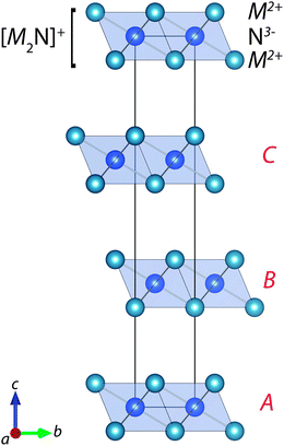 | ||
| Fig. 1 Representation of the anti-CdCl2 crystal structure adopted by the M2N series (where M = Ca, Sr, Ba), using the hexagonal setting of space group R3/m. The stacking sequence of charged M2N layers is indicated by A, B and C. | ||
One piece of circumstantial evidence for metal–metal interactions is the physical appearance of the material. For example, Ca2N crystals are “greenish black with a metallic lustre”,6 while Ba2N crystals are “black with a bluish lustre”.8 Structurally, the metal–metal distances are short (e.g. 3.2–3.6 Å in Ca2N), and indeed shorter than the typical metallic radii. However, the effective radius is greatly reduced for the cation (e.g. from 1.7 Å to 1 Å for divalent Ca).9 From explicit first-principles electronic structure calculations, including a topological analysis of the self-consistent electron density,10 we found no evidence for direct metal–metal interactions in any of the alkaline nitrides studied.
Electrides are a class of materials where electrons perform the same function as anions, i.e. a charged ion with a well-defined lattice site in the crystal structure. Localisation occurs due to the strength of the long-range electrostatic interactions, analogous to the F-centre found in alkali halides.11 In the presence of the confining electrostatic potential, a hydrogenic electronic wavefunction (Ψ) is formed at a nominally empty lattice site, with the lowest energy solution being the familiar 1s orbital. One of the most high-profile recent examples is the unconventional transparent conductor Ca24Al28O64.12 A survey of the electrostatic potential in Ca2N, performed using the GULP code,13 reveals a deep well of 11 V centred in the interlayer spacing at the special site 1/3, 2/3, 1/6 (3b Wyckoff position). This lattice site features octahedral coordination with respect to six Ca ions at a distance of 2.83 Å, consistent with the strong, localising potential. In fact, the same site is occupied by a chemical anion (halide) in the analogous ternary M2NX compounds.14 From this simple analysis, it would be expected that an electride is likely to form. The strength of the electrostatic potential has a dependence on the metal ion: it decreases for heavier metals due to the interlayer lattice expansion: for Sr and Ba, the voltage is reduced by 0.7 V and 1.0 V, respectively.
The formation of 2D electron gases at charged material interfaces and surfaces has been the subject of intensive studies in recent years; particularly involving perovskite structured oxides.15,16 To observe this phenomenon within a bulk material system would be remarkable. To favour the formation of a diffuse electronic wavefunction between charged M2N layers, the kinetic energy associated with the delocalised electronic band must be sufficient to overcome the potential energy gain due to localisation. This particular competition is well documented for the formation of small polarons.17–20 To assess these competing factors, we performed a study based on Kohn–Sham Density Functional Theory21 with semi-local (PBEsol)22 and non-local (HSE06)23 exchange–correlation functionals. The role of spin polarisation was considered, but the most stable configuration for the bulk, defect-free materials was confirmed to be a diamagnetic ground-state. The electron density from around the Fermi level of Ca2N, similar at both levels of theory, is plotted in Fig. 2. The balance between localisation and delocalisation is apparent: there is a significant density of electrons at specific lattice sites (visible at higher isosurface values), while the interaction between these sites can be visualised at lower densities (see Fig. 2b). The results are consistent with our electrostatic analysis, as well as previous studies performed at lower levels of electronic structure theory.3,24 Our work confirms that the partial electron delocalisation is not an artefact of electron self-interaction in the semi-local DFT framework.25
 | ||
| Fig. 2 Electron density isosurface (green/blue) associated with the states around the Fermi level (±0.1 eV) in Ca2N at the HSE06 level of theory. The left panel is plotted with a high isosurface value (8 me Å−3) to illustrate electron localisation around the 3b lattice site, while the right panel is plotted at a lower value (4 me Å−3) to illustrate the inter-site overlap. | ||
The interaction of the excess electrons is further quantified in the electronic band structure plotted in Fig. 3. The conduction band is formed from the interlayer “electride” orbitals with a large dispersion of almost 3 eV in the (001) plane. The band runs from Γ (Brillouin zone centre; bonding) to M (Brillouin zone edge; anti-bonding) due to the parity of the s orbital overlap. In contrast, the valence band is composed primarily from the overlap of N 2p atomic orbitals: the three N in the unit cell produce nine bands, which have moderate dispersion compared to the conduction states. From Ca2N to Ba2N, the general features of the band structure are maintained; however, the bandwidths change substantially. As the size of the metal increases, the bandwidths of both the valence and conduction bands are substantially reduced: for Ba2N this change results in the formation of an energy gap between the N 2p and electride-derived states.
 | ||
| Fig. 3 Electronic band structure at the HSE06 level of theory for (a) Ca2N, (b) Sr2N and (c) Ba2N (hexagonal space group setting), where the M → Γ vector lies in the M2N planes (along 010), while the Γ → A vector is perpendicular (along 0001). | ||
To answer the question posed in the title, the excess electrons in the metal sub-nitrides appear to exhibit a behaviour intermediate of a 2D gas and 3D electride. There is a strong localising potential, but overlap between the neighbouring orbitals is significant enough to form a dispersive Bloch wavefunction. In the absence of overlap, a dispersionless state would be expected in the electronic band structure; however, for all three materials the “electride” dispersion is greater than 2 eV. One of the physical consequences of this phenomenon will be a low activation for electron conduction. An extremely high electron mobility of 520 cm2 V−1 s−1 has been reported in Ca2N.3 The smaller electrostatic potential associated with the larger metals (Sr and Ba) should result in an even higher electron mobility. A second characteristic of electride materials is a low electron work function (or ionisation potential). For Ca2N, previous electronic structure calculations predicted a work function value lower than for Ca metal,26 which was recently confirmed by single-crystal photoemission measurements.3
Unfortunately, the enhanced electrical performance of the metal sub-nitrides comes at a chemical cost: the materials are highly reactive with both water and oxygen. In the presence of oxygen there is a colour change from black to white, consistent with spontaneous oxidation, while an explosive reaction occurs with water to produce ammonia and an oxide,7e.g.

Assessment of this reaction energy, based on ab initio thermodynamics, reveals an extremely exothermic process of the order of 700 kJ mol−1 for all three materials. Effective encapsulation will be required for any practical applications.
It remains to be seen if the optical properties of these sub-nitride electrides follow those of typical colour centres,11e.g. on-site excitation into higher energy orbitals, and doubly occupied sites with accessible singlet/triplet states. A paramagnetic signature has been reported in Ca2N,7 which suggests that they may indeed behave like F-centres. Given the potential of metal sub-nitrides for technological applications, their materials chemistry and physics deserves further investigation.
Acknowledgements
We acknowledge membership of the UK HPC Materials Chemistry Consortium, which is funded by EPSRC Grant EP/F067496, and the Materials Design Network. D.O.S. is grateful to the Ramsay Memorial Trust and University College London for the provision of a Ramsay Fellowship. A.W. acknowledges support from the Royal Society for a University Research Fellowship.References
- A. F. Wells, Structural Inorganic Chemistry, Oxford University Press, Oxford, 1984 Search PubMed.
- P. v. R. Schleyer and J. Kapp, Chem. Phys. Lett., 1996, 255, 363–366 CrossRef CAS.
- K. Lee, S. W. Kim, Y. Toda, S. Matsuishi and H. Hosono, Nature, 2013, 494, 336–340 CrossRef CAS.
- C. R. A. Catlow, Z. X. Guo, M. Miskufova, S. A. Shevlin, A. G. H. Smith, A. A. Sokol, A. Walsh, D. J. Wilson and S. M. Woodley, Philos. Trans. R. Soc., A, 2010, 368, 3379–3456 CrossRef CAS.
- P. Zapol, R. Pandey and J. D. Gale, J. Phys.: Condens. Matter, 1997, 9, 9517–9525 CrossRef CAS.
- E. T. Keve and A. C. Skapski, Inorg. Chem., 1968, 7, 1757–1761 CrossRef CAS.
- D. H. Gregory, A. Bowman, C. F. Baker and D. P. Weston, J. Mater. Chem., 2000, 10, 1635–1641 RSC.
- O. Reckeweg and F. DiSalvo, Z. Kristallogr. - New Cryst. Struct., 2005, 220, 519–520 CAS.
- R. D. Shannon, Acta Crystallogr., Sect. A: Cryst. Phys., Diffr., Theor. Gen. Crystallogr., 1976, 32, 751 CrossRef.
- R. F. W. Bader, Acc. Chem. Res., 1985, 18, 9–15 CrossRef CAS.
- A. M. Stoneham, Theory of Defects in Solids, Oxford University Press, New York, 1975 Search PubMed.
- S. Matsuishi, Y. Toda, M. Miyakawa, K. Hayashi, T. Kamiya, M. Hirano, I. Tanaka and H. Hosono, Science, 2003, 301, 626–629 CrossRef CAS.
- J. D. Gale and A. L. Rohl, Mol. Simul., 2003, 29, 291–341 CrossRef CAS.
- O. Reckeweg and F. J. DiSalvo, Solid State Sci., 2002, 4, 575–584 CrossRef CAS.
- W. Meevasana, P. D. C. King, R. H. He, S. K. Mo, M. Hashimoto, A. Tamai, P. Songsiriritthigul, F. Baumberger and Z. X. Shen, Nat. Mater., 2011, 10, 114–118 CrossRef CAS.
- J. M. Albina, M. Mrovec, B. Meyer and C. Elsasser, Phys. Rev. B: Condens. Matter Mater. Phys., 2007, 76, 165103 CrossRef.
- A. Walsh, K.-S. Ahn, S. Shet, M. N. Huda, T. G. Deutsch, H. Wang, J. A. Turner, S.-H. Wei, Y. Yan and M. M. Al-Jassim, Energy Environ. Sci., 2009, 2, 774 CAS.
- A. M. Stoneham, J. Gavartin, A. L. Shluger, A. V. Kimmel, D. Mu, D. M. Ramo, H. M. Ronnow, G. Aeppli and C. Renner, J. Phys.: Condens. Matter, 2007, 19, 255208 CrossRef.
- O. F. Schirmer, J. Phys.: Condens. Matter, 2006, 18, R667 CrossRef CAS.
- A. S. Alexandrov and N. F. Mott, Polarons and Bipolarons, World Scientific, Singapore, 1996 Search PubMed.
- W. Kohn and L. J. Sham, Phys. Rev., 1965, 140, A1133 CrossRef.
- J. P. Perdew, A. Ruzsinszky, G. I. Csonka, O. A. Vydrov, G. E. Scuseria, L. A. Constantin, X. Zhou and K. Burke, Phys. Rev. Lett., 2008, 100, 136406–136404 CrossRef.
- J. Heyd, G. E. Scuseria and M. Ernzerhof, J. Chem. Phys., 2003, 118, 8207–8215 CrossRef CAS.
- C. M. Fang, G. de Wijs, R. de Groot, H. T. Hintzen and G. de With, Chem. Mater., 2000, 12, 1847–1852 CrossRef CAS.
- J. P. Perdew and A. Zunger, Phys. Rev. B: Condens. Matter Mater. Phys., 1981, 23, 5048 CrossRef CAS.
- M. Uijttewaal, G. A. de Wijs and R. A. de Groot, J. Appl. Phys., 2004, 96, 1751–1753 CrossRef CAS.
| This journal is © The Royal Society of Chemistry 2013 |