 Open Access Article
 This Open Access Article is licensed under a Creative Commons Attribution-Non Commercial 3.0 Unported Licence
One-step technique for production of bi-functional low molecular semiconductor–polymer composites for flexible OFET applications
Tomasz
Marszalek
*,
Michal
Wiatrowski
,
Ewa
Dobruchowska†
,
Jaroslaw
Jung
and
Jacek
Ulanski
Department of Molecular Physics, Lodz University of Technology, Zeromskiego 116, 90-924 Lodz, Poland. E-mail: marszalek@mpip-mainz.mpg.de; Fax: +48 42 6313218; Tel: +48 42 6313205
First published on 2nd April 2013
Abstract
A novel one-step solution based technique to produce bi-functional semiconductor–dielectric composites for organic field effect transistor (OFET) applications has been developed. By changing the parameters and components, one can produce the composites with semiconductors on the top or at the bottom of the polymer film suitable for fabrication of OFETs with n- or p-type channels and with top and bottom configurations of electrodes.
Crystalline p- and n-type organic semiconductors are low-dimensional systems, in which high charge carrier transport is controlled either by 1D π–π stacks or by 2D transfer integrals. This implies a need for long-range order which can be realised in the form of quasi-1D long crystalline wires or quasi-2D layers with in-plane oriented platelets.1 Large area organic electronics requires technologies with only a few production steps, yielding in a reproducible way materials with well-defined morphology and properties. Therefore simple, one-batch methods for producing multifunctional, anisotropic composites are highly demanded. Such an approach requires materials with the ability of self-organisation and compatible methods for device production.
The main problem limiting the applications of organic field effect transistors (OFETs) as the driving components in flexible electronics is too low value of charge carrier mobility and too complicated, multistep methods of production. In order to obtain an organic semiconductor layer, which exhibits high charge carrier mobility, the molecular order within the layer, its morphology and properties must be designed in a way specific for a particular device. Also the dielectric film has a tremendous influence on the charge carrier mobility (μFET).2,3 One of the particularly critical problems is the implementation of n-type semiconductors in OFETs by solution based methods; only a few such transistors exhibiting high electron mobility can be found in the literature.4,5 In most cases using the n-type materials requires encapsulation of the device.6
According to the IEEE standards7 the typical procedure of fabrication of the organic transistors consists of four steps: (a) substrate preparation, (b) deposition of semiconductors, (c) deposition of dielectric, and (d) deposition of electrodes. Indeed using the conventional methods of producing OFETs from solution the dielectric and semiconductor layers are deposited in two separate steps. One of the solution based techniques is the zone-casting method, where the solution of organic semiconductor is continuously supplied through a nozzle onto a moving substrate, usually a highly doped Si wafer covered with a thin dielectric layer of SiO2,8–10 but it is also possible to use flexible substrates.11 Gradients of concentration and temperature created in the formed meniscus are the driving forces of unidirectional crystallization of the organic semiconductor in the zone-casting technique. This has inspired us to apply this technique to produce in one step bi-functional semiconductor–dielectric composites for application in OFETs. It is worth mentioning that the original zone-casting method, developed by researchers at Lodz, was used to produce from a single batch highly anisotropic conducting composites consisting of crystalline wires of charge-transfer complexes (‘organic metal’) embedded in an insulating polymer matrix.12
In this paper we present the application of the zone-casting technique to produce in one process bi-functional composites for OFET applications. Following the original concept, the common solution of the semiconductor and the polymer was continuously supplied through a flat nozzle to the moving substrate. In the formed meniscus, gradients of concentration, temperature and viscosity are created; molecules of semiconductors become gradually less mobile and progressively adopt ordered structures resulting in unidirectional crystallization of the semiconductor in the polymer matrix (Fig. 1).
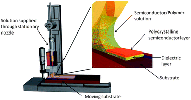 | ||
| Fig. 1 Schematic view of the zone-casting technique. | ||
The molecular structures of the used semiconducting materials and polymeric dielectric are presented in Fig. 2.
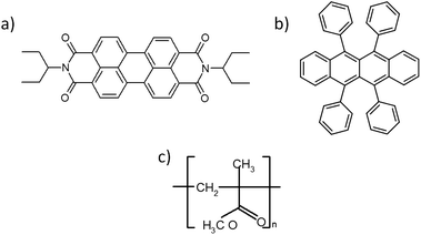 | ||
| Fig. 2 The chemical structures of low molecular semiconductors: (a) N,N-bis(1-ethylpropyl)-perylene-3,4:9,10-bis(dicarboximide) – PTCDI-C5(3), (b) 5,6,11,12-tetraphenylnaphthacene – rubrene; and polymeric dielectric: (c) poly(methyl methacrylate) – PMMA. | ||
As organic semiconductors, we have used one of the most popular p-type low molecular weight semiconductors – rubrene and also a very popular n-type semiconductor – PTCDI-C5(3); whereas as the organic dielectric, PMMA was used (Fig. 2).
The newly developed technique allows us to obtain, in one process, the composite consisting of highly oriented semiconducting crystals embedded in a polymer matrix, that serves at the same time as the dielectric and the encapsulating component. For each pair of semiconductor–polymer materials one needs to optimize the zone-casting conditions, like solution concentration, temperature of processing, rate of solution supply, height of the meniscus and speed of substrate shift.
The rubrene–PMMA composites were obtained from toluene solution with a composition of 2 mg of rubrene + 8 mg of PMMA in 1 ml of toluene. As one can see in Fig. 3, by using the zone-casting method, with properly adjusted processing parameters, we are able to produce highly oriented polycrystalline structures of rubrene embedded in a polymer matrix. Polarized optical microscope images (POM) revealed that rubrene–PMMA composites exhibit high orientation on the entire area, ca. 2 × 1 cm2.
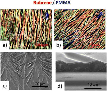 | ||
| Fig. 3 (a and b) Polarized optical microscopy images of bi-functional rubrene–PMMA composites on a glass substrate. The blue arrow indicates the casting direction; black arrows show orientations of polarization planes of the polarizer and analyzer. SEM images of the rubrene–PMMA composite: (c) surface and (d) cross-section. | ||
One can observe long crystalline needles grown along the casting direction, which proves that the rubrene molecules exhibit the tendency for unidirectional crystallization under these conditions. The POM pictures of the rubrene–PMMA composite observed for two orientations of the composites with respect to the polarization planes of the polarizers look apparently similar, as seen in Fig. 3a and b. This is probably due to the ‘herringbone’-like packing motif of the rubrene molecules in the crystal.13 Due to this specific arrangement of rubrene molecules it is difficult to observe a birefringence and absorption anisotropy of the rubrene crystals.14 SEM images of the composite surface and of the cross-section (Fig. 3c and d) demonstrate that the crystalline rubrene ‘wires’ are fully embedded in the polymer matrix. Due to such a morphology our attempts to produce OFETs with zone cast rubrene–PMMA composites were unsuccessful due to lack of contacts between the evaporated electrodes and the rubrene crystals which were covered and insulated by PMMA.
The system with the n-type semiconductor – PTCDI-C5(3)–PMMA – was obtained from chloroform solution containing 12 mg of PTCDI-C5(3) + 12 mg of PMMA in 1 ml of the solvent. The POM images (Fig. 4) confirm the unidirectional orientation of PTCDI-C5(3) crystals.
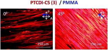 | ||
Fig. 4 Polarized optical microscopy images of bi-functional composites based on PTCDI-C5(3) with PMMA (1![[thin space (1/6-em)]](https://www.rsc.org/images/entities/char_2009.gif) :1) as a polymer matrix. The blue arrow indicates the casting direction; white arrows show orientations of polarization planes of the polarizer and analyser. :1) as a polymer matrix. The blue arrow indicates the casting direction; white arrows show orientations of polarization planes of the polarizer and analyser. | ||
The bi-layer composite zone cast on a glass substrate show birefringence when observed between crossed polarizers, indicating homogenous molecular alignment of PTCDI-C5(3) crystals (Fig. 4). Thus, one can assume that the obtained semiconducting “wires” are in fact uniaxial crystals. When the PTCDI-C5(3) crystal optic axis is parallel to the polarization plane of the polarizer or analyzer, almost no light is transmitted through the sample, however when the crystal optic axis is oriented at ca. 45° with respect to the polarization planes of both polarizers, maximum transmission of light is observed.
From the point of view of potential applications for OFET construction, the composites with n-type semiconductors are especially attractive, therefore further work was focused on optimization of the preparation conditions for the PTCDI-C5–PMMA system, aiming to achieve bi-layer composites in which the crystalline PTCDI-C5 wires grow on or under the polymer surface. The chloroform solutions with different relative PTCDI-C5(3) to PMMA content ratios: 1:4; 2:4 and 3:4 were prepared and used for zone-casting.
SEM images of the 1:4 composite show, that continuous PTCDI-C5(3) crystalline wires are embedded in the PMMA matrix (Fig. 5a). Thus one can assume that the polymer matrix will work simultaneously as the gate dielectric and also as the encapsulating coating.
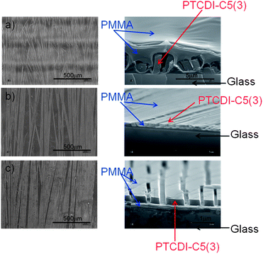 | ||
| Fig. 5 The surface and cross-sectional SEM images for PTCDI-C5(3)–PMMA samples with different compositions: (a) 1:4, (b) 2:4, and (c) 3:4, respectively. | ||
However, not all parts of the crystalline wires are covered by the polymer, as one can see on the magnified SEM image of the surface (Fig. 6). Due to such discontinuities in the polymer ‘coating’ one can get contacts with the semiconductor wires by evaporation of the metal electrodes.
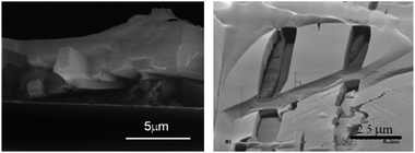 | ||
| Fig. 6 The surface and cross-sectional SEM images of the PTCDI-C5(3)–PMMA composite (1:1). | ||
Fig. 5b and c present SEM pictures of the PTCDI-C5(3)–PMMA (2:4) and (3:4) composites, in which the semiconductor crystalline wires are formed on the surface of the layer (Fig. 5c), making them accessible for metal contacts evaporated onto the surface. Differences in morphology between the rubrene–PMMA and PTCDI-C5(3)–PMMA composites result probably from differences in polymer–additive interactions: rubrene is partially soluble in the PMMA, so it starts to crystallise relatively late, when the polymer solution has high viscosity, and the growing crystals remain in the polymer matrix. In contrast, PTCDI-C5(3) starts to crystallize earlier, and the crystals are pushed out from the thin solution.
The OFET devices were fabricated from the PTCDI-C5(3)–PMMA composites zone-cast on the glass substrate. The glass was cleaned in an ultrasonic bath using chloroform and isopropanol successively for 10 minutes each. After the cleaning, the gold electrode (gate) was deposited by vacuum evaporation. Using this substrate the anisotropic PTCDI-C5(3)–PMMA (1:1) composite was deposited by the zone casting method with the following parameters: solutions were supplied through a flat nozzle with a rate of 0.23 μl s−1; the substrate was moving with a velocity of 50 μm s−1; the substrate and the nozzle were thermally stabilized at 30 °C. Then the source and the drain electrodes were deposited by subsequent vacuum evaporation of aluminium and silver (150 nm thick each); the channel length was L = 100 μm, and the channel width was W = 2 mm. The channel length was oriented along the zone-casting direction, i.e. along the PTCDI-C5(3) crystalline wires. The produced OFETs with top contacts, bottom gate configurations were measured in air at room temperature using the Keithley 2410 analyzer driven by the adapted Matlab program. The capacitance of the gate dielectric was determined by dielectric spectroscopy measurements (CONCEPT 80 dielectric spectrometer, Novocontrol GmbH, Germany).
Fig. 7 presents the output characteristics of OFETs based on bi-functional PTCDI-C5(3)–PMMA composites. The linear regime of the output characteristics (marked by the dotted circles) shows an obvious contact-resistance effect. This effect is probably caused by a not perfect contact between the evaporated electrodes and the semiconductor crystals, covered partially by the polymer. On the other hand, we should remember that the PTCDI-C5(3) is not stable in air and due to this reason the thin polymeric layer on the crystals surface works as an encapsulating layer. The mobility calculated for the top contacts, bottom gate devices were in the range 0.1–1 cm2 V−1 s−1 which is a relatively high value for the n-type OFETs obtained by the solution-based method. The OFET parameters were calculated from the saturation region for UGS = 16 V, in which the maximum current IDS = 0.005 is observed with a relatively low on/off ratio of around 25. The low value of on/off ratio could be caused by the high density of amorphous semiconductor phase in a polymer matrix. Further optimization of the composites morphology and OFET structure, in particular improvements of the contacts between the electrodes and the semiconductor, should yield OFETs with better working parameters and reproducibility.
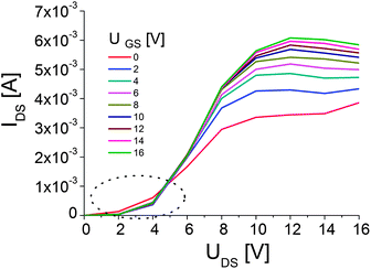 | ||
| Fig. 7 Output characteristics of OFET based on PTCDI-C5(3)–PMMA (1:1) composites. | ||
Conclusions
In summary, we have demonstrated that zone-casting is a solution based technique that allows us to produce in a one batch process bi-functional composites for OFET applications. We have found that by changing the zone cast parameters it is possible to produce composites with semiconductors on the top or at the bottom of the polymer matrix. Using this technique one can produce OFETs also based on unstable semiconductors by encapsulating them already during the fabrication process. This method can be applied for various pairs of organic semiconductors and polymeric dielectrics; the main requirement is that the polymer and semiconductor should exhibit solubility in the same solvent. It should be noted, however, that one still needs to elaborate the technique of deposition of the source and drain electrodes which would form ohmic contacts; one can anticipate, for example, that conducting inks, with suitable solvent, can penetrate the polymer and ensure ohmic contacts with the semiconductor crystals embedded in the polymer matrix.Acknowledgements
This work was partially supported by following grants: NoE PolyNet and NoE FlexNet projects of 7FR EU and START project of Foundation for Polish Science and N N507 399939 of Polish Ministry of Science.Notes and references
- H. Sirringhaus, P. J. Brown, R. H. Friend, M. M. Nielsen, K. Bechgaard, B. M. W. Langeveld-Voss, A. J. H. Spiering, R. A. J. Janssen, E. W. Meijer, P. Herwig and D. M. de Leeuw, Nature, 1999, 401, 685 CrossRef CAS.
- A. Facchetti, M.-H. Yoon and T. J. Marks, Adv. Mater., 2005, 17, 1705 CrossRef CAS.
- R. P. Ortiz, A. Facchetti and T. J. Marks, Chem. Rev., 2010, 110, 205 CrossRef CAS.
- I. Tszydel, M. Kucinska, T. Marszalek, R. Rybakiewicz, A. Nosal, J. Jung, M. Gazicki-Lipman, C. Pitsalidis, C. Gravalidis, S. Logothetidis, M. Zagorska and J. Ulanski, Adv. Funct. Mater., 2012, 22, 3840 CrossRef CAS.
- J. Soeda, T. Uemura, Y. Mizuno, A. Nakao, Y. Nakazawa, A. Facchetti and J. Takeya, Adv. Mater., 2011, 23, 3681 CrossRef CAS.
- Y. Wen and Y. Liu, Adv. Mater., 2010, 22, 1331 CrossRef CAS.
- 1620 IEEE Standard Test Methodes for the Characterization of Organic Transistors and Materials, IEEE Std 1620TM-2004.
- W. Pisula, A. Menon, M. Stepputat, I. Lieberwirth, U. Kolb, A. Tracz, H. Sirringhaus, T. Pakula and K. Mullen, Adv. Mater., 2005, 17(6), 684 CrossRef CAS.
- S. Kotarba, J. Jung, A. Kowalska, T. Marszalek, M. Kozanecki, P. Miskiewicz, M. Mas-Torrent, C. Rovira, J. Veciana, J. Puigmarti-Luis and J. Ulanski, J. Appl. Phys., 2010, 108, 014504 CrossRef.
- P. Miskiewicz, M. Mas-Torrent, J. Jung, S. Kotarba, I. Glowacki, E. Gomar-Nadal, D. B. Amabilino, J. Veciana, B. Krause, D. Carbone, C. Rovira and J. Ulanski, Chem. Mater., 2006, 18, 4724 CrossRef CAS.
- T. Marszalek, A. Nosal, R. Pfattner, J. Jung, S. Kotarba, M. Mas-Torrent, B. Krause, J. Veciana, M. Gazicki-Lipman, C. Crickert, G. Schmidt, C. Rovira and J. Ulanski, Org. Electron., 2012, 13, 121 CrossRef CAS.
- J. Ulanski and M. Kryszewski, “Reticulate Composites" in The Encyclopedia of Advanced Materials, ed. D. Bloor, R. J. Brook, M. C. Flemings, S. Mahajan, R. W. Cahn, Pergamon Press, Oxford, 1994, vol. 3, pp. 2301–2306 Search PubMed.
- S. Bergantin and M. Moret, Cryst. Growth Des., 12, 6035 CAS.
- N. Stingelin-Stutzmann, E. Smits, H. Wondergem, C. Tanase, P. Blom, P. Smith and D. De Leeuw, Nat. Mater., 2005, 4, 601 CrossRef CAS.
Footnote |
| † Present address: Institute of Technology and Education, Koszalin University of Technology, Sniadeckich 2, 75-453 Koszalin, Poland. Fax: 48 94 3486652; Tel: 48 94 3486651. |
| This journal is © The Royal Society of Chemistry 2013 |