Two-dimensional semiconductors: recent progress and future perspectives
Abstract
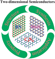
Graphene with a sp2-honeycomb carbon lattice has drawn a large amount of attention due to its excellent properties and potential applications in many fields. Similar to the structure of graphene, two-dimensional semiconductors are its two-dimensional and isostructural counterparts based on the typical layer-structured semiconductors, such as boron nitride (h-BN) and transition metal dichalcogenides (e.g. MoS2 and WS2), whose layers are bound by weak van der Waals forces. Unlike the semi-metal features of graphene, the two-dimensional semiconductors are natural semiconductors with thicknesses on the atomic scale. When one of the dimensions is extremely reduced, the two-dimensional semiconductors exhibit some unique properties, such as a transition from indirect to direct semiconductor properties, and hence have great potential for applications in electronics, energy storage, sensors, catalysis and composites, which arise both from the dimension-reduced effect and from the modified electronic structure. In this feature article, recent developments in the synthesis, properties and applications of two-dimensional semiconductors are discussed. The reported virtues and novelties of two-dimensional semiconductors are highlighted and the current problems in their developing process are clarified, in addition to their challenges and future prospects.


 Please wait while we load your content...