 Open Access Article
 This Open Access Article is licensed under a
 Creative Commons Attribution 3.0 Unported Licence
Direct extreme UV-lithographic conversion of metal xanthates into nanostructured metal sulfide layers for hybrid photovoltaics†
Thomas
Rath
*a,
Celestino
Padeste
b,
Michaela
Vockenhuber
b,
Christopher
Fradler
ac,
Matthias
Edler
d,
Angelika
Reichmann
e,
Ilse
Letofsky-Papst
e,
Ferdinand
Hofer
e,
Yasin
Ekinci
b and
Thomas
Griesser
d
aInstitute for Chemistry and Technology of Materials, Graz University of Technology, Stremayrgasse 9, 8010 Graz, Austria. E-mail: thomas.rath@tugraz.at
bLaboratory for Micro- and Nanotechnology, Paul Scherrer Institute, 5232 Villigen PSI, Switzerland
cChristian Doppler Laboratory for Nanocomposite Solar Cells, Graz University of Technology, Stremayrgasse 9, 8010 Graz, Austria
dChair of Chemistry of Polymeric Materials & Christian Doppler Laboratory for Functional and Polymer Based Inkjet Inks, University of Leoben, Otto Glöckel-Strasse 2, 8700 Leoben, Austria
eInstitute for Electron Microscopy and Nanoanalysis, Graz University of Technology & Graz Centre for Electron Microscopy, Steyrergasse 17, 8010 Graz, Austria
First published on 30th July 2013
Abstract
We present a versatile strategy toward the preparation of nanostructured metal sulfide layers, which exploits the photosensitivity of metal xanthates as a powerful tool for lithographic structuring. Using extreme ultraviolet interference lithography (EUV-IL), we successfully realized well-defined column and comb nanostructures. This approach provides new pathways to fabricate highly ordered structured metal sulfide layers with periodicities far below 100 nm for potential application in hybrid solar cells.
Organic–inorganic hybrid solar cells based on conjugated polymers and inorganic semiconducting nanostructures are currently a field of intensive research because of their promising properties due to combined advantages of both organic and inorganic semiconductors. A large variety of organic and inorganic materials may be blended to form bulk heterojunction absorber layers for hybrid solar cells.1,2 Most prominent examples are combinations of a conjugated polymer with CdSe,3 CdS,4 CuInS2,5 PbS,6 or ZnO.7 To date, maximum power conversion efficiencies (PCEs) between 4 and 5% have been reported for organic–inorganic hybrid solar cells.4,8 One very promising strategy to further improve the PCE of hybrid solar cells is to modify the bulk heterojunction toward a more ordered morphology. Ordered heterojunction structures of the organic and the inorganic component, which are vertically bicontinuous and interdigitized, can significantly improve charge transport properties, while maintaining a high interfacial area.9
In fully organic polymer/[6,6]-phenyl C61 butyric acid methyl ester (PCBM) solar cells, such ordered bulk heterojunctions are mainly prepared using nanoimprint lithography (NIL) to pattern the polymer layer, which is infiltrated by PCBM.9,10 In the case of hybrid material systems, mainly the inorganic semiconductor is patterned and infiltrated with the organic donor material.10 Nanostructured hybrid solar cells have been realized so far with several material classes including mostly metal oxides10,11 as well as e.g. silicon12–14 or gallium arsenide.15 The nanostructures were typically prepared by (template assisted) nanorod or nanotube growth, etching, or selected area epitaxy processes.
To date, ordered polymer/metal sulfide heterojunctions have not been explored at all. This may originate from the fact that only a very limited number of methods for the preparation of nanostructured metal sulfide layers exists, even though semiconducting metal sulfides are a very important class of materials which are widely used in hybrid as well as in inorganic thin film solar cells. Furthermore, they are important in a wide range of further applications like waveguides, sensors, photodetectors, electroluminescent devices or photocatalysts, where nanostructured layers can be beneficial.16–19 While, in particular in hybrid solar cells, structured metal sulfide layers can find prospective application for the formation of a well-defined ordered heterojunction in the absorber layer to enhance device performance,10 in inorganic thin film solar cells, nanostructured layers can be used as light trapping layers to optimize absorption properties,20 or to improve carrier collection.21
So far, structured metal sulfide layers have been mainly prepared by lithographic patterning of functional surface molecule layers or self-assembled monolayers on the substrate followed by selective growth or deposition of the metal sulfide16,17,22–24via electron-beam lithography (EBL)25,26 or by molecular printing techniques.27,28 Following the first method, the organic layer remains between metal sulfide layer and substrate after structuring, which may limit possible applications of the nanostructured layers. With the latter mentioned methods only very small areas can be structured in a reasonable time.
In this work, we introduce an exciting strategy for the fabrication of column structures as well as comb structures showing periodicities of 140 nm with the potential to reach periodicities far below 100 nm. The nanostructures are achieved by direct patterning and thus, the fabrication process does not involve pattern transfer such as lift-off or etching. In this route metal xanthates are used as precursors, which can be thermally converted to metal sulfides,5,29 but also by UV-light.30 This offers the possibility of the formation of structured metal sulfide layers via a photochemically induced solid state reaction. The used metal xanthates show strong absorption at wavelengths below 300 nm leading to their decomposition and subsequent formation of the corresponding metal sulfides upon UV- or extreme UV (EUV)-illumination under reduced pressure. We demonstrate the potential of this method with the semiconducting metal sulfide copper indium sulfide (CIS), a well-known absorber material in thin film photovoltaics, which has also already been successfully incorporated in organic–inorganic hybrid solar cells.5
Fig. 1 shows FT-IR spectra of a layer containing a mixture of copper and indium xanthates before and after UV illumination (mercury medium pressure lamp). The characteristic peaks of the xanthates (for a detailed assignment see Table S1 in the ESI†) vanished completely after 20 min of UV-illumination. The concerted formation of the copper indium sulfide is proved by the selected area electron diffraction (SAED) pattern of a sample after UV-illumination. The SAED pattern shows diffraction rings, indicating that the sample is nanocrystalline and that the crystals have no preferential order. The positions of the main diffraction rings (112, r = 3.19 nm−1; 200, r = 3.70 nm−1; 204/220, r = 5.21 nm−1; 116/312, r = 6.11 nm−1) are in good agreement with reference data for chalcopyrite CIS (PDF 27-159). The principle possibility of the formation of nanocrystalline CuInS2 solely by UV-treatment of precursors is in agreement with a report by Nairn et al.31 who prepared CuInS2 nanocrystals in an organic solvent by photochemical decomposition of a single-source metal–thiolate precursor.
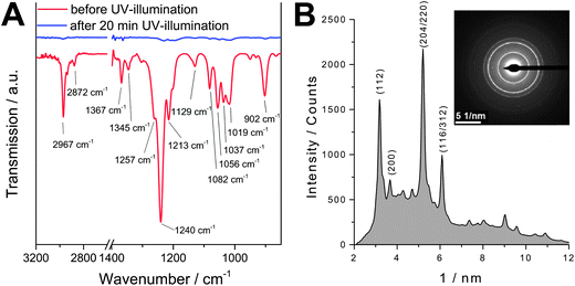 | ||
| Fig. 1 (A) FT-IR spectra of a metal xanthate precursor layer before and after 20 min UV-illumination under reduced pressure; (B) SAED image and the corresponding radial intensity profile of the UV-illuminated sample. | ||
Furthermore, scanning electron microscopy-energy dispersive X-ray (SEM-EDX) measurements were conducted to analyze the chemical composition of the nanocrystalline CIS layer formed by photolysis of the metal xanthates. The EDX spectrum reveals a copper/indium molar ratio of about 1/1.6, which is close to the copper/indium ratio of the precursor layer (1/1.7). A surplus of indium is necessary as this leads to n-type CIS,32 which is essential for application of this material in hybrid solar cells, as only n-type CIS leads to well performing polymer/CIS hybrid solar cells.5,33
The formation of copper indium sulfide is additionally confirmed by X-ray photoelectron spectroscopy (XPS). The corresponding spectra of a metal xanthate precursor film before and after UV-illumination as well as after thermal treatment are presented in Fig. 2. The XPS-signals of the photochemically prepared CIS layer match well with a thermally (195 °C) converted reference sample and for all elements shifts in binding energy between precursor layer and CIS layer are observed. For the elements Cu and In, the binding energies between the precursor layer and the UV-treated sample are shifted about 1 eV to higher energy. For S, the peak is shifted about 0.5 eV to the lower energy region. In the photochemically prepared sample, the binding energies of Cu2p1/2 and Cu2p3/2 are 952.6 and 932.9 eV, those of In3d3/2 and In3d5/2 are 452.6 and 445.1 eV and for S2p a binding energy of 162.1 eV is measured. The found binding energies match very well with reference data for CIS from the literature.34
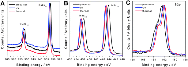 | ||
| Fig. 2 XPS spectra of the elements Cu (A), In (B) and S (C) in the precursor film (black), after thermal annealing (red) and after UV-treatment (blue). | ||
The presented data show that it is possible to produce crystalline copper indium sulfide thin films in a solid state reaction by UV-treatment of a precursor layer. This opens up the unique possibility of photolithographic structuring of metal sulfide layers. In this structuring process, the metal xanthate precursor can be viewed as a negative resist. UV-illuminated areas are cured and become insoluble due to the formation of the metal sulfide, while the non-illuminated areas remain readily soluble in organic solvents. The principle of the photolithographic structuring process using metal xanthate precursor layers is schematically shown in Fig. 3.
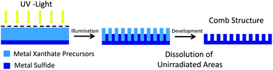 | ||
| Fig. 3 Schematic illustration of the photolithographic process for the preparation of metal sulfide comb structures from metal xanthates. | ||
To realize a comb structure as shown in Fig. 3, in the first step, a thin and continuous CIS layer is prepared by thermal or UV-conversion from metal xanthates on a suitable substrate. Subsequently, a metal xanthate precursor layer, which is coated from a solution onto the first CIS layer, is UV-illuminated through a shadow mask. Thus, CIS is formed in the illuminated areas, which leads to shrinkage in volume due to the evaporation of the volatile decomposition products of the metal xanthates5 and an increase in density in the material. Finally, the structure is developed by short dipping of the substrate into an organic solvent like chloroform or toluene leading to dissolution of the unexposed xanthate.
Using standard UV-photolithography, we could realize comb structures with periodicities down to 5 μm using contact masks. However, for many applications including also the application in absorber layers of organic/inorganic hybrid solar cells, much smaller structures (periodicities of 20–200 nm) are desired. To achieve structures far below 1 μm, we identified extreme ultraviolet interference lithography (EUV-IL) to be an ideally suited method for this purpose. Also laser interference lithography (LIL), as well as EBL,26 were considered as generally suitable techniques. However, compared to LIL, EUV-IL has the advantage that resolutions far below 100 nm can be achieved. Resolutions in this range would also be possible with EBL, but using this method, the throughput is limited due to the serial nature of EBL.
In contrast to this, EUV-lithography is currently considered to be the next-generation technique for high-volume semiconductor chip production with feature sizes down to the sub-10 nm region.35,36 Interference lithography using EUV radiation gained increasing attention in academic as well as industrial research as a powerful tool providing high resolution, high throughput, and large-area patterning,37,38 which makes this technique also highly interesting for our application.
In initial series of EUV-IL experiments, we used a “multi-pattern mask” which offered the possibility of creating various structures (dots and lines) and periodicities during one exposure using two- and four-beam interference schemes. Besides exposure times, also the thickness of the precursor layer had to be optimized before impressively homogeneous column-like structures with periodicities of 283 nm as well as 141 nm could be achieved. AFM and SEM images of the prepared nanostructures are shown in Fig. 4. The height of the nano-columns is about 29–35 nm (corresponding height profiles are included in the ESI, Fig. S2†).
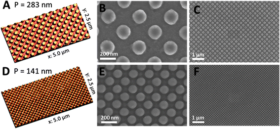 | ||
| Fig. 4 AFM images (A and D) and SEM micrographs (B, C, E, and F) with different magnifications of copper indium sulfide column structures with periodicities of 283 nm (A–C) and 141 nm (D–F) prepared via four-beam interference. The height of the structures is about 29–35 nm. | ||
Regarding future application of these nanostructured layers in absorber layers of hybrid solar cells, the column structures were not fabricated on silicon substrates, which would be the standard substrates for EUV-IL, but they are already prepared on the layer structure glass/ITO/TiOx/CdS (see the Methods section) which can be directly implemented in hybrid solar cells with inverse device architecture.39 Prior to the lithographic preparation of the structured CIS layer from the Cu- and In-xanthate precursor layer, a 5 nm thin continuous CIS layer was applied on the glass/ITO/TiOx/CdS layer stack. By the introduction of this thin CIS layer, it is provided that the conjugated polymer, with which the nanostructured CIS layer is infiltrated to form an interdigitized network of donor and acceptor in the absorber layer, does not have direct contact with the subjacent layer. This would adversely influence the electronic properties of the final device. After infiltration with a conjugated polymer, the preparation of hybrid solar cells can be finished by applying a PEDOT:PSS layer and metal electrodes. Keeping in mind that the nanostructured layers are prepared on a stack of multiple solution-processed layers, the achieved nanostructures are impressively well defined and homogeneous (see Fig. 4F).
The smallest gap between two columns in the sample with the periodicity of 141 nm (Fig. 4D–F) is about 35 nm. This is already quite close to an ideal feature size for efficient charge separation in hybrid bulk heterojunctions, which would be approximately 20 nm, the doubled exciton diffusion length in conjugated polymers.10 The fact that the structures, even with these very small gaps, are clearly separated and well defined strongly suggests that the realization of even smaller structure sizes should be possible by further optimization. Thus, the pre-conditions for a successful incorporation of EUV-lithographically structured metal sulfide layers, having feature sizes close to the exciton diffusion length, in absorber layers of hybrid solar cells are fulfilled and future research will be directed to this topic.
The discussed column structures were achieved via four-beam interference. Keeping in mind that the metal xanthate resist needs a comparably long exposure time for curing, column structures were easier to realize than line structures, which are reached by interference of two beams, leading to lower intensity. Using standard EUV-IL masks, line structures could not be prepared using exposure times of up to 4 minutes (dose ∼ 8000 mJ cm−2). We note that this value is the dose on the mask level and the dose on the wafer level is about 5–10% of this value due to the diffraction efficiency of the grating and absorption of the supporting SiN membrane of the masks. To achieve the goal of realizing line structures and to overcome the above-mentioned challenges of exposure time, we also worked with the ASFM (achromatic spatial frequency multiplication) technique in further experiments. In this technique, which is based on the achromatic Talbot effect, all transmitted light contributes to image formation leading to much higher efficiency, but also to higher background intensity.40 This means that exposure times are considerably shorter, however, they have to be most accurately adjusted, as overexposure leads to curing of the full area, and underexposure only to curing in surface-near areas of the film, which leads to full removal of the film during the developing step. Fortunately, metal xanthates appear to provide a well suited sensitivity curve and CIS comb structures with a periodicity of 280 nm could be prepared using an exposure dose of less than 5000 mJ cm−2.
AFM as well as SEM images of the line-structures are presented in Fig. 5. The comb-structure is regular and has a height difference of 25 nm, as measured with AFM (for the corresponding height profile see Fig. S3 in the ESI†). Using the ASFM technique, areas of 1 × 1 mm2 were structured in one exposure step and even bigger nanostructured areas can be easily realized by stitching or using a scan exposure mode.41
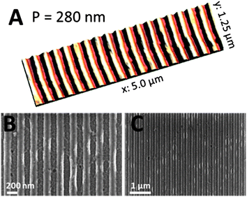 | ||
| Fig. 5 AFM image (A) and SEM micrographs (B and C) with different magnifications of copper indium sulfide comb structures with a periodicity of 280 nm and a structure height of 25 nm. | ||
In conclusion, we presented a versatile strategy for the preparation of nanostructured metal sulfide layers using metal xanthate precursors. We identified the photosensitivity of metal xanthates as a powerful tool for lithographic structuring and successfully realized column as well as comb structures with a periodicity of 140 nm using EUV-IL and we certainly see the potential to achieve nanostructures with resolutions far below 100 nm. To tackle this problem, on the one hand, optimization of the metal xanthate precursor materials (variation of the alkyl chains) will be necessary in order to reduce the volume shrinkage and to increase their sensitivity to UV-illumination, which will also help to reduce remaining carbon in the nanostructured material. On the other hand, further optimization of the EUV-IL exposure, also including testing of new masks with higher resolution may enable realization of nanostructures with sizes of a few ten nanometers.
Experimental details
Sample preparation and UV-illumination
The used metal xanthates (copper O-2,2-dimethylpentan-3-yl-dithiocarbonate and indium O-2,2-dimethylpentan-3-yl-dithiocarbonate) were synthesized according to a previously published procedure.5 The precursor layers were prepared via spin coating from chlorobenzene solutions on silicon substrates covered with a thin CIS layer or on glass/ITO substrates covered with TiOx, CdS and CIS layers. The TiOx layer was prepared by doctor blading a titanium diisopropoxide bis(acetylacetonate)-precursor dissolved in isopropanol and subsequent annealing of the substrate at 450 °C under ambient conditions, the CdS as well as the CIS layer were formed by thermal conversion (160 °C and 195 °C, respectively) of the corresponding metal xanthates. For photochemical conversion, the metal xanthate layers were illuminated in a quartz glass tube under reduced pressure (approx. 10 mbar) using an Omnicure S1000 lamp (1.1 W cm−2, measured with a spectroradiometer, Solatell, Sola Scope 2000 TM, spectral range from 230 to 400 nm).Extreme UV (EUV) interference lithography
Samples coated with metal xanthate layers were exposed to EUV light at the XIL-II beamline of the Swiss Light Source (SLS). Exposure was performed in a vacuum (<5 × 10⁻⁶ mbar). The beamline uses undulator light with a central wavelength of 13.5 nm (92.5 eV photon energy) and 4% spectral bandwidth. The incident EUV power on the mask was about 30 mW cm−2 and the exposure time in the range of up to 5 minutes was controlled using a beam shutter. Structure definition was achieved by irradiation through silicon nitride masks with chromium gratings of different periods and arrangements21 or through gold-plated ASFM masks.40Characterization techniques
The thicknesses of the layers were characterized on a Bruker Dektak XT surface profiler. IR-spectroscopy was performed on a Perkin Elmer Spectrum One. XPS studies were done using a K-Alpha photoelectron spectrometer (Thermo Scientific). AFM measurements were carried out in TappingMode® in air on a Dimension IIIa instrument (Veeco, Germany). The AFM images were analyzed using WSxM software (Nanotec Electronica).42 SEM characterizations were done on a Zeiss Ultra 55 equipped with an EDAX Phoenix detector for EDX measurements. SAED was performed on a FEI Tecnai 12 electron microscope.Acknowledgements
Financial support from the Christian Doppler Research Association, the Austrian Federal Ministry of Economy, Family and Youth (BMWFJ), and ISOVOLTAIC AG is gratefully acknowledged. The authors thank Gregor Trimmel and Mario Arar for valuable and helpful discussions and Lukas Troi for technical help. Part of this work was performed at the Swiss Light Source, Paul Scherrer Institute, Villigen, Switzerland.References
- Y. Zhou, M. Eck and M. Krüger, Energy Environ. Sci., 2010, 3, 1851 CAS.
- R. Zhou and J. Xue, ChemPhysChem, 2012, 13, 2471 CrossRef CAS.
- K. F. Jeltsch, M. Schädel, J.-B. Bonekamp, P. Niyamakom, F. Rauscher, H. W. A. Lademann, I. Dumsch, S. Allard, U. Scherf and K. Meerholz, Adv. Funct. Mater., 2012, 22, 397 CrossRef CAS.
- S. Ren, L.-Y. Chang, S.-K. Lim, J. Zhao, M. Smith, N. Zhao, V. Bulovic, M. Bawendi and S. Gradecak, Nano Lett., 2011, 11, 3998 CrossRef CAS.
- T. Rath, M. Edler, W. Haas, A. Fischereder, S. Moscher, A. Schenk, R. Trattnig, M. Sezen, G. Mauthner, A. Pein, D. Meischler, K. Bartl, R. Saf, N. Bansal, S. A. Haque, F. Hofer, E. J. W. List and G. Trimmel, Adv. Energy Mater., 2011, 1, 1046 CrossRef CAS.
- J. Seo, M. J. Cho, D. Lee, A. N. Cartwright and P. N. Prasad, Adv. Mater., 2011, 23, 3984 CrossRef CAS.
- S. D. Oosterhout, M. M. Wienk, S. S. van Bavel, R. Thiedmann, L. J. A. Koster, J. Gilot, J. Loos, V. Schmidt and R. A. J. Janssen, Nat. Mater., 2009, 8, 818 CrossRef CAS.
- Z. Chen, H. Zhang, X. Du, X. Cheng, X. Chen, Y. Jiang and B. Yang, Energy Environ. Sci., 2013, 6, 1597 CAS.
- Y. Yang, K. Mielczarek, M. Aryal, A. Zakhidov and W. Hu, ACS Nano, 2012, 6, 2877 CrossRef CAS.
- J. Weickert, R. B. Dunbar, H. C. Hesse, W. Wiedemann and L. Schmidt-Mende, Adv. Mater., 2011, 23, 1810 CrossRef CAS.
- G. K. Mor, S. Kim, M. Paulose, O. K. Varghese, K. Shankar, J. Basham and C. A. Grimes, Nano Lett., 2009, 9, 4250 CrossRef CAS.
- S. Jeong, E. C. Garnett, S. Wang, Z. Yu, S. Fan, M. L. Brongersma, M. D. McGeehe and Y. Cui, Nano Lett., 2012, 12, 2971 CrossRef CAS.
- K.-Q. Peng and S.-T. Lee, Adv. Mater., 2011, 23, 198 CrossRef CAS.
- S.-C. Shiu, J.-J. Chao, S.-C. Hung, C.-L. Yeh and C.-F. Lin, Chem. Mater., 2010, 22, 3108 CrossRef CAS.
- G. Mariani, Y. Wang, P.-S. Wong, A. Lech, C.-H. Hung, J. Shapiro, S. Prikhodko, M. El-Kady, R. B. Kaner and D. L. Huffaker, Nano Lett., 2012, 12, 3581 CrossRef CAS.
- P. Lu and A. V. Walker, ACS Nano, 2009, 3, 370 CrossRef CAS.
- X. Meng, Y. Lu, B. Yang, G. Yi and J. Jia, ACS Appl. Mater. Interfaces, 2010, 2, 3467 CAS.
- H. Lin, H. Liu, X. Qian, S.-W. Lai, Y. Li, N. Chen, C. Ouyang, C.-M. Che and Y. Li, Inorg. Chem., 2011, 50, 7749 CrossRef CAS.
- X. Fang, L. Wu and L. Hu, Adv. Mater., 2011, 23, 585 CrossRef CAS.
- S. Mokkapati and K. R. Catchpole, J. Appl. Phys., 2012, 112, 101101 CrossRef.
- J. Jean, S. Chang, P. R. Brown, J. J. Cheng, P. H. Rekemeyer, M. G. Bawendi, S. Gradecak and V. Bulovic, Adv. Mater., 2013, 25, 2790 CrossRef CAS.
- F. F. Amos, S. A. Morin, J. A. Streifer, R. J. Hamers and S. Jin, J. Am. Chem. Soc., 2007, 129, 14296 CrossRef CAS.
- Y. K. Hwang, S. Y. Woo, J. H. Lee, D.-Y. Jung and Y.-U. Kwon, Chem. Mater., 2000, 12, 2059 CrossRef CAS.
- Y. Lu, S. Liang, M. Chen and J. Jia, J. Colloid Interface Sci., 2009, 332, 32 CrossRef CAS.
- B. Radha, S. Kiruthika and G. U. Kulkarni, J. Am. Chem. Soc., 2011, 133, 12706 CrossRef CAS.
- L. Persano, A. Camposeo, F. Di Benedetto, R. Stabile, A. M. Laera, E. Piscopiello, L. Tapfer and D. Pisignano, Adv. Mater., 2012, 24, 5320 CrossRef CAS.
- L. R. Giam, S. He, N. E. Horwitz, D. J. Eichelsdoerfer, J. Chai, Z. Zheng, D. Kim, W. Shim and C. A. Mirkin, Nano Lett., 2012, 12, 1022 CrossRef CAS.
- H. Chu, L. Ding, J. Wang, X. Li, L. You and Y. Li, J. Phys. Chem. C, 2008, 112, 18938 CAS.
- J. M. Clark, G. Kociok-Köhn, N. J. Harnett, M. S. Hill, R. Hill, K. C. Molloy, H. Saponia, D. Stanton and A. Sudlow, Dalton Trans., 2011, 40, 6893 RSC.
- M. Tejos, B. G. Rolón, R. del Río and G. Cabello, Mater. Sci. Semicond. Process., 2008, 11, 94 CrossRef CAS.
- J. J. Nairn, P. J. Shapiro, B. Twamley, T. Pounds, R. von Wandruszka, T. R. Fletcher, M. Williams, C. Wang and M. G. Norton, Nano Lett., 2006, 6, 1218 CrossRef CAS.
- H. J. Lewerenz, Sol. Energy Mater. Sol. Cells, 2004, 83, 395 CrossRef CAS.
- E. Maier, T. Rath, W. Haas, O. Werzer, R. Saf, F. Hofer, D. Meissner, O. Volobujeva, S. Bereznev, E. Mellikov, H. Amenitsch, R. Resel and G. Trimmel, Sol. Energy Mater. Sol. Cells, 2011, 95, 1354 CrossRef CAS.
- M. C. Zouaghi, T. B. Nasrallah, S. Marsillac, J. C. Bernède and S. Belgacem, Thin Solid Films, 2001, 382, 39 CrossRef CAS.
- C. Wagner and N. Harned, Nat. Photonics, 2010, 4, 24 CrossRef CAS.
- B. Päivänranta, A. Langner, E. Kirk, C. David and Y. Ekinci, Nanotechnology, 2011, 22, 375302 CrossRef.
- V. Auzelyte, C. Dais, P. Farquet, D. Grützmacher, L. H. Heyderman, F. Luo, S. Olliges, C. Padeste, P. K. Sahoo, T. Thomson, A. Turchanin, C. David and H. H. Solak, J. Micro/Nanolithogr., MEMS, MOEMS, 2009, 8, 021204 CrossRef.
- L. Wang, B. Terhalle, V. A. Guzenko, A. Farhan, M. Hojeij and Y. Ekinci, Appl. Phys. Lett., 2012, 101, 093104 CrossRef.
- S. Dowland, T. Lutz, A. Ward, S. P. King, A. Sudlow, M. S. Hill, K. C. Molloy and S. A. Haque, Adv. Mater., 2011, 23, 2739 CrossRef CAS.
- L. Wang, B. Terhalle, M. Hojeij, V. A. Guzenko and Y. Ekinci, J. Vac. Sci. Technol., B, 2012, 30, 031603 Search PubMed.
- L. Wang, H. H. Solak and Y. Ekinci, Nanotechnology, 2012, 23, 305303 CrossRef CAS.
- I. Horcas, R. Fernández, J. M. Gómez-Rodriguez, J. Colchero, J. Gómez-Herrero and A. M. Baro, Rev. Sci. Instrum., 2007, 78, 013705 CrossRef CAS.
Footnote |
| † Electronic supplementary information (ESI) available: Fig. S1–S3 and Table S1. See DOI: 10.1039/c3ta12592k |
| This journal is © The Royal Society of Chemistry 2013 |