 Open Access Article
 This Open Access Article is licensed under a Creative Commons Attribution-Non Commercial 3.0 Unported Licence
Polydopamine-assisted decoration of ZnO nanorods with Ag nanoparticles: an improved photoelectrochemical anode†
Yuefan
Wei‡
a,
Junhua
Kong‡
b,
Liping
Yang
b,
Lin
Ke
c,
Hui Ru
Tan
c,
Hai
Liu
b,
Yizhong
Huang
b,
Xiao Wei
Sun
d,
Xuehong
Lu
*b and
Hejun
Du
*a
aSchool of Mechanical and Aerospace Engineering, Nanyang Technological University, 50 Nanyang Avenue, Singapore 639798. E-mail: MHDU@ntu.edu.sg
bSchool of Materials Science and Engineering, Nanyang Technological University, 50 Nanyang Avenue, Singapore 639798. E-mail: asxhlu@ntu.edu.sg
cInstitute of Materials Research & Engineering, A-star, 3 Research Link, Singapore 117602
dSchool of Electric and Electronic Engineering, Nanyang Technological University, 50 Nanyang Avenue, Singapore 639798
First published on 12th February 2013
Abstract
The modification of zinc oxide (ZnO) with silver (Ag) has proven to be an effective strategy to enhance the optical and electrical properties, in which the interactions between ZnO and Ag are critically determined by the structure and morphology of the ZnO–Ag hybrids. In order to achieve homogeneous and controllable distribution, polydopamine (PDA) was introduced via in situpolymerization to assist the decoration of ZnO nanorods (NRs) with Ag nanoparticles (NPs). Compared with pristine ZnO NRs, the light absorption is significantly enhanced for the PDA assisted Ag-decorated ZnO, which is attributed to the Ag NPs as well as the carbonized PDA thin film. Ag NPs of small size enhance the multiple/high-angle scattering from localized plasmonic effect, which increases the light path length hence traps more light. The carbonized PDA film is further beneficial to the absorption of the visible light. The Ag-decorated ZnO NRs on fluorine-doped tin oxide (FTO) coated glasses were then used as photoanodes of the photoelectrochemical (PEC) cell. The short circuit current density (JSC, 1.8 mA cm−2), maximum photo current conversion efficiency (PCE, 3.9%) and lifetime (3.07 mA cm−2 at 500 seconds) are achieved with an optimized loading of Ag nanoparticles derived from 0.01 M silver nitrate (AgNO3), which are found to be much higher than those of pristine ZnO NRs and other reported Ag–ZnO-based photoanodes. The overall PEC performance improvement is attributed to the localized plasmonic effect enhanced light harvesting as well as the facilitated charge transport and inhibition of recombination of electrons and holes from both Ag nanoparticles that act as an electron acceptor and carbonized PDA film as stabilizer and separator.
Introduction
Photocatalytic water splitting through converting sunlight into a green energy source, hydrogen, is considered as one of the most promising techniques in energy production. Nanostructured zinc oxide (ZnO) is widely used as a photoanode in this area due to the good processability, excellent electrochemical stability and high electron mobility of ZnO,1 as well as the nanosize-induced large surface area. One-dimensional (1D) ZnO, which possesses a higher aspect ratio than the zero-dimensional (0D) one, offers additional advantages of faster electron transport.2 Yet, the unsatisfying photon absorption and high surface electron–hole recombination rate act as inhibitors of its practical use in such a photo-related area where optical properties play a crucial role. Efforts to address these issues for 1D ZnO include alloying with other materials to form multi-bandgap structures,3dye and quantum dots sensitization,4–7 and metal nanocrystals incorporation.Incorporation of metal nanocrystals, such as Ag, Au, Al, Co and Ce8–12 on photovoltaic materials has shown great superiority on improving the performance over the other strategies. Ag is one of the most promising metals among all, due to its good chemical stability and highest electrical conductivity,13,14 and therefore it plays an important role in collecting and concentrating electrons into current of photovoltaic cells. Moreover, based on the localized surface plasmon resonance, the interactions between incident light and noble metallic nanoparticles result in the oscillation of the free electrons. This plasmon oscillation leads to stronger light scattering and enhancement to the photovoltaic effect. Thus, Ag is also intensively investigated as a back mirror and designed into different nanostructures as surface modification to concentrate the sunlight. Indeed, the decoration of ZnO with Ag would alter the optical and electrical properties of such a ZnO–Ag system. It is believed that the size control of Ag and geometric arrangement of Ag in the ZnO matrix would significantly affect the interactions with the incident light and induced properties. Depending on the preparation methods, the architecture of ZnO–Ag hybrids varies. Some typical examples include incorporating Ag nanoparticles (NPs) into ZnO nanofibers through electrospinning;15 doping Ag into a ZnO thin film via pneumatic spray pyrolysis (PSP) technique,16 or into ZnO spheres via microwave-assisted synthesis;17 obtaining worm-like Ag–ZnO core–shell hybrids through ultrasonic irradiation;18 depositing Ag NPs onto ZnO nanorods (NRs) via photo deposition,19 plasma enhanced chemical vapor deposition,20electrodeposition,21 seed-mediated method,22 or electron beam evaporation.23 Despite the various routes to attach Ag NPs onto ZnO nanostructures, the attachment is uneven and uncontrollable, therefore hardly effective to utilize the interactions-induced plasmonic effect, and only a few of these studied the effect on photoelectrochemical (PEC) water splitting. Tarwal and Patil synthesized a Ag-doped ZnO thin film via PSP technique.16 The photocurrent density obtained at 0 V was 249 μA cm−2 in visible light and 303 μA cm−2 in UV illumination. Xie's group prepared Ag–ZnO photocatalysts through the photocatalytic reduction of Ag+ on ZnO.24 A photocurrent density of 80 μA cm−2 was achieved at 0 V under UV illumination. Lin's group reported a photocatalytic nanosystem comprising an Ag core covered with an approximately 2 nm thick nanoshell of Ag3(PO4)1−x on the ZnO NRs.25 The maximum photo current conversion efficiency (PCE) was 2% with a photocurrent of 3.1 mA cm−2 at +0.6 V.
Polydopamine (PDA), derived from self-polymerization of dopamine in alkaline aqueous solutions, is a synthetic polymer, which has excellent affinity to most of solid surfaces.26 Due to the strong tendency to form coating on the surfaces as well as the feasibility to adjust its thickness from a few nanometers to tens of micrometers,27,28 a coating of PDA would be a promising route to functionalize the hosts. In this work, the Ag NPs were evenly deposited onto ZnO NRs with the assistance of PDA coating, utilizing the capability of PDA in reducing AgNO3 to Ag.29,30 The PEC properties of the Ag-decorated ZnO NRs were investigated and correlated to the morphology.
Experimental
Materials
Dopamine chloride (DOPA), tris-(hydroxymethyl) aminomethane (Tris) and zinc acetate dihydrate (Zn(CH3COO)2·2H2O) were purchased from Sigma chemistry (USA). Zinc nitrate hexahydrate (ZnN2O6·6H2O), AgNO3, ammonia hydroxide (NH3·H2O) and sodium sulphate (Na2SO4) were supplied by Sigma-Aldrich (Germany). Ethanol (C2H5OH) was purchased from Merck Chemicals (Germany).Preparation of ZnO nanorods
ZnO NRs were synthesized via a hydrothermal process. The Zn(CH3COO)2·2H2O–ethanol solution (0.0005 M) was firstly deposited on fluorine-doped tin oxide (FTO) coated glass (25 × 25 mm2) viaspin coating (3000 rpm) for 30 seconds followed by annealing at 350 °C for 30 minutes. The annealed substrate was then hydrothermally treated at 90 °C for 24 hours in 80 mL of ZnN2O6·6H2O aqueous solution (0.04 M). The aqueous solution was neutralized by NH3·H2O before hydrothermal treatment. The obtained ZnO NRs array on FTO glass was rinsed with deionized (DI) H2O and dried at 60 °C in vacuum for 24 hours.Coating with polydopamine thin film
FTO glass coated with ZnO NRs was dipped vertically into 80 mL of Tris aqueous buffer solution (0.01 M). 24 mg of DOPA (0.0016 M) was dissolved in the above solution under gentle magnetic stirring. The system was then kept still for 2 hours at room temperature to allow in situ coating. The coated sample, which was denoted as ZnO–D, was finally rinsed with DI H2O for further treatment.Deposition of Ag nanoparticles
The Ag nanoparticles were deposited onto PDA-coated ZnO NRs via a simple dip/redox process. In a typical experiment, the as-prepared sample was vertically immersed into 80 mL of AgNO3 aqueous solution and kept still for 2 hours at room temperature. The treated ZnO NRs array was then rinsed with DI H2O and gently blown with nitrogen flow. After drying at 60 °C in vacuum for 24 hours, the sample was annealed at 500 °C in argon flow (100 sccm) for 3 hours. Following this procedure, AgNO3 solutions with concentrations of 0, 0.005, 0.01, 0.05 and 0.1 M were used to deposit various amounts of Ag. The samples were denoted as ZnO–C, ZnO–C–0.005Ag, ZnO–C–0.01Ag, ZnO–C–0.05Ag and ZnO–C–0.1Ag, corresponding to the 0, 0.005, 0.01, 0.05 and 0.1 M AgNO3 solution, respectively.Characterization
The morphologies of samples were studied using a field-emission scanning electron microscope (FESEM, JEOL 6700) and a transmission electron microscope (TEM, JEOL 2100). The elemental mapping was carried out using scanning TEM-energy dispersive X-ray spectroscopy (STEM-EDX). The electron tomography of the nanostructures was carried out using an FEI Titan 80-300 STEM which is equipped with a high-angle annular dark-field (HAADF) detector, a probe aberration corrector and a single-tilt tomography holder. The size distribution of the Ag nanoparticles was measured statistically on obtained TEM images using ImageJ (100–200 nanoparticles). The structures of samples were characterized using wide-angle X-ray diffraction (WAXD, Bruker D8 Discover GADDS X-ray diffractometer). The optical properties of the samples were studied using a spectrophotometer (LAMBDA 950 UV/Vis/NIR PerkinElmer) under the wavelength range of 250–800 nm. The PEC properties were investigated using a three-electrode system with the prepared ZnO NRs as the working electrode. Pt foil and a standard Ag/AgCl electrode were used as the counter and reference electrodes, respectively. Na2SO4 aqueous solution (0.5 M) was used as the electrolyte and was purged with N2 for 5–10 minutes before the test. The J–V test was carried out in a voltage window of −0.5 to 1.0 V and a scanning rate of 0.1 V s−1 using electrochemical workstation (Autolab, PGSTAT302). The working electrode was exposed to an UV spot light source (Lightingcure™, model LC-5, from Hamamatsu Photonics, France, cf. Fig. S1† for light spectrum). The power density of the yielded illumination was 100 mW cm−2. The lifetime test was conducted at a constant voltage of 0.5 V under illumination.Results and discussion
Morphologies and structures
The preparation procedures for PDA-assisted deposition of Ag NPs onto ZnO NRs are shown in Scheme 1. ZnO NRs with diameters of less than 100 nm and lengths of around 1 μm were grown on the FTO coated glass (cf. Fig. S2†). PDA film was uniformly deposited onto the surface of the ZnO NRs via a simple immersion/in situpolymerization route. The strong affinity of PDA to ZnO, as aforementioned, ensures a PDA coating with a thickness of around 5–8 nm under the designed conditions (cf. Fig. S3†). The PDA-coated ZnO NRs were then used to capture Ag NPs, in which the PDA film acts as a reductant to reduce AgNO3 to metallic Ag as well as “glue” to anchor the Ag NPs. An annealing process was conducted to convert the PDA film into a carbonaceous one and refine the crystallinity of the Ag NPs without destroying the attachment.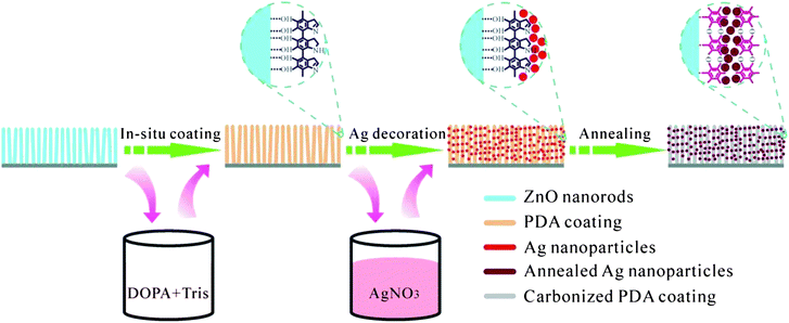 | ||
| Scheme 1 A schematic demonstration of polydopamine (PDA)-assisted Ag nanoparticles decorated on ZnO nanorods. | ||
The success of the PDA coating and Ag NPs capture is indicated by the visual color change upon the in situ coating and reduction as shown in Fig. 1. The incorporation of Ag is confirmed by the WAXD results, which are shown in Fig. 2. The peak at about 26.5° (peak A) can be assigned to hexagonal SnO2 from the FTO substrate, while that at around 37.7° (peak B) is the overlapping of SnO2 and Ag. The area ratio of peak B to peak A increases with the increase of concentration of the AgNO3 precursor solution, indicating the successful incorporation of Ag into ZnO NRs.
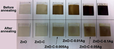 | ||
| Fig. 1 The photos of pristine ZnO nanorods (NRs) and the ones decorated with PDA coating and Ag nanoparticles before and after annealing. | ||
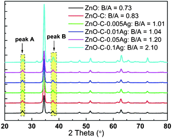 | ||
| Fig. 2 Wide-angle X-ray diffraction (WAXD) spectrum of pristine ZnO NRs and Ag nanoparticles-decorated ZnO NRs with different Ag loading. | ||
The morphologies of the Ag NPs-decorated ZnO NRs with various Ag loading are shown in Fig. 3. The loading of Ag is determined by the concentration of AgNO3 solution ranging from 0.005 M to 0.1 M, while maintaining the reduction time. As can be seen from the FESEM (Fig. 3a1–d1) and TEM images (Fig. 3a2–d2), Ag nanoparticles, most of which are less than 50 nm in size, are homogeneously adhered to the surface of ZnO NRs. The size distribution of the Ag NPs in different samples is shown in Fig. 4. It confirms the small size (<50 nm) and indicates that the size of the Ag nanoparticles is in an incremental trend with the increasing AgNO3 solution concentration. The geometrical arrangement of ZnO and Ag is confirmed by the HADDF-STEM and STEM-EDX elemental mapping results, taking ZnO–C–0.01Ag as a typical example (Fig. 5). The nanoparticle loading increases distinctly with the increase of AgNO3 solution concentration, from a limited number of nanoparticles (ZnO–C–0.005Ag) to large area coverage (ZnO–C–0.1Ag).
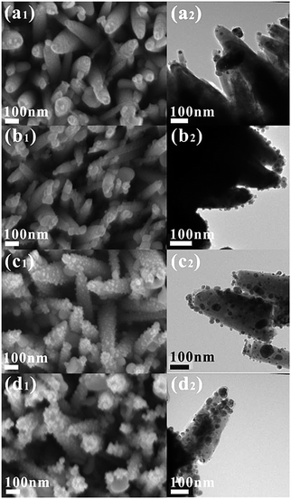 | ||
| Fig. 3 Morphology (left: field-emission scanning electron microscope (FESEM), middle and right: transmission electron microscope (TEM)) of Ag nanoparticle-decorated ZnO NRs after annealing from an AgNO3 concentration of (a1 and a2) 0.005, (b1 and b2) 0.01, (c1 and c2) 0.05 and (d1 and d2) 0.1 M. | ||
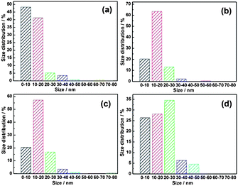 | ||
| Fig. 4 The size distribution of Ag nanoparticles in (a) ZnO–C–0.005Ag, (b) ZnO–C–0.01Ag, (c) ZnO–C–0.05Ag and (d) ZnO–C–0.1Ag. | ||
 | ||
| Fig. 5 (a) High-angle annular dark-field scanning TEM (HAADF STEM) and (b1–b5) scanning TEM-energy dispersive X-ray spectroscope (STEM-EDX) elemental mapping results of ZnO–C–0.01Ag. | ||
The geometry and structure of the nanostructures were further investigated by high-resolution TEM (HRTEM) and HAADF-TEM, taking ZnO–C–0.01Ag as a typical example. The HRTEM image and the diffraction pattern, as shown in Fig. 6a and b, indicate that each Ag nanoparticle is a single crystal with interlayer spacing of 0.23 nm for plane (111) and the carbonized PDA coating, which wraps the ZnO NRs, has a thickness of 3–5 nm after annealing. The reduction of the film thickness after annealing is due to the shrinkage of PDA upon removal of the heteroatoms including H, O and N. Different from the ones before annealing, in which the attached Ag NPs are naked (Fig. S4†), the Ag NPs are fully covered by the carbonized PDA film with a thickness of 2–3 nm in the ZnO–C–Ag system after annealing. This is due to the diffusion of PDA along with the solid surface during the annealing process that leads to carbonized PDA covering the solid surface, which is a common phenomenon for carbon materials. The carbonized PDA film is in a layered structure, which is consistent with our previous observation.27 The covering of Ag nanoparticles by PDA is further confirmed by the HADDF-STEM EDX line scanning results, as shown in Fig. 6c. The intensity of Ag and the carbon signal gets stronger and stronger from point A to B to C, indicating the existence of both carbon and Ag in the nanoparticles. It is believed that Ag NPs and ZnO NRs are separated from each other by the PDA film due to the sequence of PDA coating followed by Ag NPs decoration during preparation process. The separation was confirmed by the TEM results as shown in Fig. 7, where the layered PDA film can be clearly observed between the Ag nanoparticle and ZnO matrix. The distance between the two is around 3 nm. In this case, the interactions between Ag and ZnO are very much different from those with direct contact, which will be discussed in the following section.
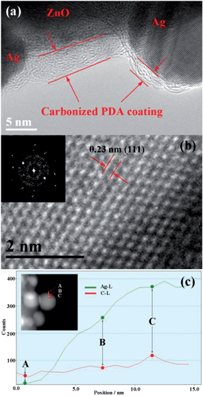 | ||
| Fig. 6 (a) High-resolution TEM (HRTEM) of ZnO–C–0.01Ag, showing the PDA coating. (b) Atomic resolved HRTEM of a single Ag nanoparticle, showing the structure of Ag nanoparticle. Inset shows the corresponding diffraction pattern. (c) The HADDF-STEM EDX line scanning results on a single Ag nanoparticle. | ||
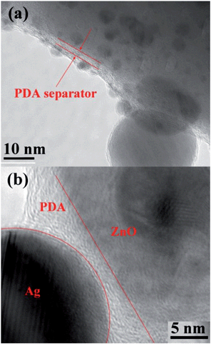 | ||
| Fig. 7 (a) TEM and (b) HRTEM images of ZnO–C–0.01Ag, showing the PDA film that acts as a separator. | ||
Herein, a heterostructure of Ag nanoparticles-decorated ZnO NRs with controllable Ag loading and small Ag NPs of less than 50 nm is formed via the assistance of PDA coating. The direct immersion of bare ZnO NRs array into Ag-containing solution will introduce Ag into array, whereas the Ag nanoparticles tend to fall down to the interspaces of ZnO NRs rather than being anchored to the surface of ZnO NRs, forming a random and uncontrollable morphology (cf. Fig. S5†). This indicates the critical role of the PDA film in stabilizing the attachment of Ag NPs onto ZnO NRs. Moreover, the carbonized PDA film may change the charge transport behavior in the formed heterostructure due to the coverage of Ag NPs and the separation between Ag and ZnO by PDA coating, which will be discussed in the following section.
Optical properties
The optical properties of the ZnO–C–Ag heterostructures were investigated with the results shown in Fig. 8. Fig. 8a shows the total reflection spectrum, which includes mirror-like (specular) reflection and scattering (diffusion) from the samples. As in our case, the surfaces of the prepared samples are rough and can be considered to be completely non-reflective dominant, i.e., perfectly diffusive. Compared with pure ZnO NRs, ZnO–C shows a similar reflection trend in the UV light region, but lower reflection in the visible light region. However, ZnO–C–Ag presents higher reflection than that from ZnO–C, which is attributed to the enhanced scattering reflection from the Ag NPs embedded in the carbonized PDA matrix. The reflection trap at around 318 to 323 nm can be assigned to the intrinsic transition band of Ag, indicating effective interactions among incident light, Ag and ZnO.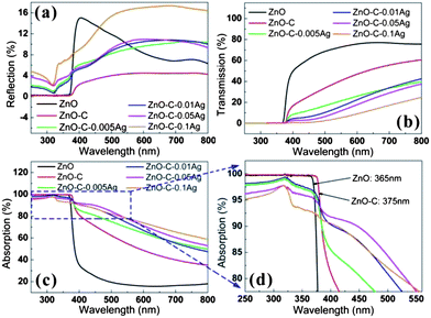 | ||
| Fig. 8 (a) Reflection, (b) transmission and (c) absorption of Ag-decorated ZnO NRs with different Ag nanoparticles loading, (d) the enlarged profile of the area highlighted with a blue window in (c). | ||
As demonstrated in the morphological analysis, Ag NPs with sizes of 10–50 nm are embedded into the carbonized PDA thin film. The embedded Ag NPs can therefore exhibit a strong scattering of incident light and result in intense light absorption, which can be interpreted as localized surface plasmonic effect.31 Compared with bare ZnO NRs, the reflection fluctuation of modified ZnO NRs, including ZnO–C and ZnO–C–Ag with various Ag loading, is less than 10%. Among all the ZnO–C–Ag samples, ZnO–C–0.1Ag exhibits obviously the highest light reflection, indicating that the strongest light scattering occurs at the Ag-embedded carbonized PDA layer.
Fig. 8b shows the transmission spectrum. The light transmission from ZnO–C is reduced by about 20% within the visible light range compared with that of the pristine ZnO NRs. Upon the deposition of Ag NPs, the transmission from ZnO–C–Ag is further decreased by at least 20%. Fig. 8c shows the absorption spectrum, which is calculated by subtracting the reflection and transmission from the total incident light. For pure ZnO NRs, the sharp absorption edge at 365–375 nm is attributed to electronic transition of ZnO. A 10 nm red-shift of absorption edge (Fig. 8d), from 365 nm to 375 nm, is observed for ZnO–C, which is due to the carbonized PDA coating acting as carbon doping.32–34 This indicates higher sensitivity of ZnO–C NRs to visible light. The carbonized PDA film, which is considered as multi-layered graphite with doped heteroatoms according to our previous work,27 can assist in absorbing extra visible light. Therefore, higher absorption of carbonized PDA-coated ZnO NRs (ZnO–C) than that of pristine ZnO NRs is observed within the light range of 400–800 nm (Fig. 8c).
The absorption of Ag NPs-decorated ZnO NRs within the visible light ranging from 380 to 800 nm is further strengthened compared with that of bare ZnO and ZnO–C. This is attributed to, on the one hand, the localized surface plasmonic resonance between Ag and ZnO that is featured in strong light absorbing as aforementioned.35,36 It is proven that the interaction between the incident light and the larger spherical Ag NPs with sizes of 10–50 nm gives rise to a very efficient resonant photon scattering, which largely increases the direct light absorption of ZnO NRs.37 On the other hand, strong light scattering is induced from the interaction of the incident light and Ag NPs, which helps lengthen the optical path and further reduces the light energy loss. It is worth noting that no distinct absorption enhancement is observed when increasing the Ag deposition, which is due to higher reflection at higher Ag loading as verified in Fig. 8a. It is therefore suggested that a relatively low Ag loading would be adequate to ensure effective light–Ag–ZnO interactions.
Photoelectrochemical performance
The PEC properties of ZnO–C–Ag heterostructures as a photoanode were investigated and shown in Fig. 9. Since no photocurrent is generated in the dark environment, the photocurrent produced is derived from the electron–hole pairs which are excited by the solar energy. Compared with pristine ZnO NRs, the Ag NPs decorated ZnO NRs show significantly higher photocurrent density under illumination. As can be seen from Fig. 9a, the short circuit current density, which is defined as the one at zero potential vs. the reference electrode,38 is only 0.3 mA cm−2 for pristine ZnO NRs, while it is 1.3 mA cm−2 for ZnO–C–0.005Ag and 1.8 mA cm−2 for ZnO–C–0.01Ag. Further increase of the Ag loading induces a short circuit, which sucks the electrons. Therefore higher photo-excited current density is not achievable even with higher Ag loading (Fig. S6†).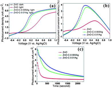 | ||
| Fig. 9 (a) Photocurrent density–voltage (J–V) characteristic, (b) photo current conversion efficiency (PCE) and (c) working lifetime of Ag nanoparticles-decorated ZnO NRs with different Ag loading in dark/light. | ||
The PCE, which is calculated using the same method as in other reports,39–41 of all the samples is shown in Fig. 9b. The maximum PCE of pristine ZnO NRs is 1.5% (0.51 V), while that of ZnO–C–0.005Ag is 3.6% (0.26 V), and that of ZnO–C–0.01Ag is 3.9% (0.22 V), corresponding to an improvement of about 2.5 times. Upon applying a constant voltage (0.5 V), the photocurrent density of pristine ZnO NRs suffers rapid decay to 0.66 mA cm−2 at 500 s (Fig. 9c), while that of the Ag NPs-decorated ZnO NRs remains as high as 2.21 and 3.07 mA cm−2, for ZnO–C–0.005Ag and ZnO–C–0.01Ag, respectively. Even after 1800 s, the photocurrent density of ZnO–C–Ag is more than 2 times higher than that of pristine ZnO NRs, indicating a much better lifetime for the Ag NPs-decorated ZnO NRs. The significant improvement of PEC properties, as compared with pristine ZnO NRs and other reported Ag–ZnO-based photoanodes,16,24,25 indicates that the PDA-assisted uniform decoration of ZnO NRs with Ag NPs is an effective strategy to form a ZnO–Ag heterostructure for PEC applications.
The improvement of PEC performance of Ag NPs-decorated ZnO NRs is attributed to the strengthened light trapping capability as presented above, the facilitated charge transport, as well as the inhibition of electron–hole recombination. First, the incorporation of Ag NPs into ZnO NRs leads to increased light absorption, which helps to generate more light-induced electron–hole pairs from ZnO NRs, as well as the intense local electric fields formed around the Ag NPs, which reinforce the separation of the electron–hole pairs, especially in the vicinity of the Ag NPs, i.e. the surface of the ZnO NRs. The surface potential plays a role in separating the electron–hole pairs generated,42 shifts the electrons to the counter electrode and moves the holes to the surface of the working electrode. Second, the designed nanostructure facilitates the effective charges transport. In the prepared ZnO–C–Ag heterostructures, the Ag NPs are separated from ZnO NRs through the carbonized PDA film with thickness of around 3 nm acting as stabilizer and separator. Different from the other ZnO–Ag systems with direct contact, in which the charge transport is realizable, the carbonized PDA film in the obtained ZnO–C–Ag heterostructures inhibits the direct transfer of photo-excited electrons from ZnO to Ag. Instead, energy transfer from Ag NPs to ZnO NRs is generated.43 Third, the overall charge carrier concentration is therefore increased in the ZnO NRs,44 leading to higher photocurrent density and longer lifetime. Moreover, the Ag NPs are covered by the carbonized PDA film with graphite-like layered structure. The two-dimensional planar π-conjugation, as verified previously,27 may additionally inhibit the recombination of electrons and holes. Furthermore, the layered-structure can act as a supporter to facilitate the effective transport of the photo-excited electrons.2,41,42 This further strengthens the efficiency of the photoanode in water splitting.
Conclusions
In summary, PDA film-assisted Ag NPs-decorated ZnO NRs with uniform and controllable Ag loading have been successfully prepared viahydrothermal method followed by in situ coating and dip/redox capture. The PDA film acts as a reducing agent to produce Ag NPs and a stabilizer to anchor their attachment onto ZnO NRs. The ZnO–C–Ag heterostructure exhibits excellent light harvesting due to the localized surface plasmonic effect and the additional light absorption from carbonized PDA film. Much higher photocurrent density, larger PCE and longer lifetime are achieved in comparison with pristine ZnO NRs and other reported Ag–ZnO hybrids when the ZnO–C–Ag heterostructure is used as a photoanode. The improvement is due to the induced excellent light trapping capability, the facilitated charge transport as well as the inhibition of electron–hole recombination from Ag NPs and carbonized PDA film. This work offers an effective strategy to introduce Ag NPs into ZnO, which are separated from each other through a graphite-like multi-layered phase for improved PEC properties.Notes and references
- S. Baruah and J. Dutta, Sci. Technol. Adv. Mater., 2009, 10, 013001 CrossRef.
- H. M. Chen, C. K. Chen, R. S. Liu, L. Zhang, J. Zhang and D. P. Wilkinson, Chem. Soc. Rev., 2012, 41, 5654 RSC.
- H. Kim, M. Seol, J. Lee and K. Yong, J. Phys. Chem. C, 2011, 115, 25429 CrossRef CAS.
- J. J. Kim, K. S. Kim and G. Y. Jung, J. Mater. Chem., 2011, 21, 7730 RSC.
- J. Xu, X. Yang, Q.-D. Yang, T.-L. Wong, S.-T. Lee, W.-J. Zhang and C.-S. Lee, J. Mater. Chem., 2012, 22, 13374 RSC.
- H. M. Chen, C. K. Chen, Y. C. Chang, C. W. Tsai, R. S. Liu, S. F. Hu, W. S. Chang and K. H. Chen, Angew. Chem., Int. Ed., 2010, 49, 5966 CAS.
- N. Chouhan, C. L. Yeh, S. F. Hu, R. S. Liu, W. S. Chang and K. H. Chen, Chem. Commun., 2011, 47, 3493 RSC.
- J. Xie and Q. Wu, Mater. Lett., 2010, 64, 389 CrossRef CAS.
- Y. Qiu, W. Chen, S. Yang, B. Zhang, X. X. Zhang, Y. C. Zhong and K. S. Wong, Cryst. Growth Des., 2010, 10, 177 CrossRef CAS.
- X. Zeng, J. Yuan and L. Zhang, J. Phys. Chem. C, 2008, 112, 3503 CrossRef CAS.
- C. Y. Wang, C. P. Liu, H. W. Shen, Y. J. Chen, C. L. Kuo, T. Y. Wang, R. K. Zheng and S. P. Ringer, J. Phys. Chem. C, 2010, 114, 18031 Search PubMed.
- H.-C. Gong, J.-F. Zhong, S.-M. Zhou, B. Zhang, Z.-H. Li and Z.-L. Du, Superlattices Microstruct., 2008, 44, 183 CrossRef CAS.
- Z. C. Wang and G. Chumanov, Adv. Mater., 2003, 15, 1285 Search PubMed.
- G. Merga, L. C. Cass, D. M. Chipman and D. Meisel, J. Am. Chem. Soc., 2008, 130, 7067 CrossRef CAS.
- D. D. Lin, H. Wu, R. Zhang and W. Pan, Chem. Mater., 2009, 21, 3479 CrossRef CAS.
- N. L. Tarwal and P. S. Patil, Electrochim. Acta, 2011, 56, 6510 Search PubMed.
- L. B. Wang, Q. K. Hu, Z. Y. Li, J. Y. Guo and Y. W. Li, Mater. Lett., 2012, 79, 277 Search PubMed.
- H. R. Liu, G. X. Shao, J. F. Zhao, Z. X. Zhang, Y. Zhang, J. Liang, X. G. Liu, H. S. Jia and B. S. Xu, J. Phys. Chem. C, 2012, 116, 16182 Search PubMed.
- C. L. Ren, B. F. Yang, M. Wu, J. A. Xu, Z. P. Fu, Y. Lv, T. Guo, Y. X. Zhao and C. Q. Zhu, J. Hazard. Mater., 2010, 182, 123 CrossRef CAS.
- M. Macias-Montero, A. Borras, Z. Saghi, P. Romero-Gomez, J. R. Sanchez-Valencia, J. C. Gonzalez, A. Barranco, P. Midgley, J. Cotrino and A. R. Gonzalez-Elipe, J. Mater. Chem., 2012, 22, 1341 RSC.
- K. Zhong, Y. C. Mao, X. F. Sun, C. L. Liang, P. Liu and Y. X. Tong, J. Electrochem. Soc., 2012, 159, K161 Search PubMed.
- X. T. Yin, W. X. Que, D. Fei, F. Y. Shen and Q. S. Guo, J. Alloys Compd., 2012, 524, 13 Search PubMed.
- Y. F. Wei, L. Ke, J. H. Kong, H. Liu, Z. H. Jiao, X. H. Lu, H. J. Du and X. W. Sun, Nanotechnology, 2012, 23, 235401 Search PubMed , (8pp).
- W. Xie, Y. Z. Li, W. Sun, J. C. Huang, H. Xie and X. J. Zhao, J. Photochem. Photobiol., A, 2010, 216, 149 CrossRef CAS.
- Y. G. Lin, Y. K. Hsu, Y. C. Chen, S. B. Wang, J. T. Miller, L. C. Chen and K. H. Chen, Energy Environ. Sci., 2012, 5, 8917 RSC.
- H. Lee, S. M. Dellatore, W. M. Miller and P. B. Messersmith, Science, 2007, 318, 426 CrossRef CAS.
- J. Kong, W. A. Yee, L. Yang, Y. Wei, S. L. Phua, H. G. Ong, J. M. Ang, X. Li and X. Lu, Chem. Commun., 2012, 48, 10316 RSC.
- L. Yang, W. A. Yee, S. L. Phua, J. Kong, H. Ding, J. W. Cheah and X. Lu, RSC Adv., 2012, 2, 2208 RSC.
- S. M. Kang, S. Park, D. Kim, S. Y. Park, R. S. Ruoff and H. Lee, Adv. Funct. Mater., 2011, 21, 108 CrossRef CAS.
- W. C. Wang, A. N. Zhang, L. Liu, M. Tian and L. Q. Zhang, J. Electrochem. Soc., 2011, 158, D228 CrossRef CAS.
- C. F. Bohren and D. R. Huffman, Absorption and Scattering of Light by Small Particles, WILEY-VCH Verlag GmbH & Co. KGaA, Canada, 2007, pp. 280–324 Search PubMed.
- S. T. Tan, X. W. Sun, Z. G. Yu, P. Wu, G. Q. Lo and D. L. Kwong, Appl. Phys. Lett., 2007, 91, 072101 CrossRef.
- X. J. Ye, C. S. Liu, W. Zhong, H. A. Song, C. T. Au and Y. W. Du, Phys. Lett. A, 2010, 374, 496 CrossRef CAS.
- X. Zhou, Y. Z. Li, T. Peng, W. Xie and X. J. Zhao, Mater. Lett., 2009, 63, 1747 CrossRef CAS.
- J. M. Luther, P. K. Jain, T. Ewers and A. P. Alivisatos, Nat. Mater., 2011, 10, 361 CrossRef CAS.
- K. A. Willets and R. P. Van Duyne, Localized Surface Plasmon Resonance Spectroscopy and Sensing, in Annual Review of Physical Chemistry, 2007, vol. 58, p. 267 Search PubMed.
- S. Link and M. A. El-Sayed, J. Phys. Chem. B, 1999, 103, 8410 CrossRef CAS.
- J. Shi, Y. Hara, C. L. Sun, M. A. Anderson and X. D. Wang, Nano Lett., 2011, 11, 3413 CrossRef CAS.
- S. Bin Dolmanan, L. Szu Cheng, K. Lin, L. Wei Wei, J. Zhi Hui and S. Xiao Wei, IEEE Electron Device Lett., 2010, 31, 734 Search PubMed.
- Z. Chen, T. F. Jaramillo, T. G. Deutsch, A. Kleiman-Shwarsctein, A. J. Forman, N. Gaillard, R. Garland, K. Takanabe, C. Heske and M. Sunkara, J. Mater. Res., 2011, 25, 3 Search PubMed.
- S. U. M. Khan, M. Al-Shahry and W. B. Ingler Jr, Science, 2002, 297, 2243 CrossRef CAS.
- T. Bak, J. Nowotny, M. Rekas and C. C. Sorrell, Int. J. Hydrogen Energy, 2002, 27, 991 CrossRef CAS.
- D. B. Ingram and S. Linic, J. Am. Chem. Soc., 2011, 133, 5202 CrossRef CAS.
- P. Christopher, D. B. Ingram and S. Linic, J. Phys. Chem. C, 2010, 114, 9173 CrossRef CAS.
Footnotes |
| † Electronic supplementary information (ESI) available: The light spectrum of the light source, morphology of ZnO nanorods grown on FTO coated glass, morphology of polydopamine (PDA) film on ZnO nanorods, TEM images of Ag nanoparticles-decorated ZnO nanorods before annealing, morphology of Ag nanoparticles on ZnO nanorods prepared from direct immersion of bare ZnO nanorods into Ag-containing solution, photocurrent density–voltage (J–V) characteristic of Ag nanoparticles-decorated ZnO nanorods with higher Ag nanoparticles loading. See DOI: 10.1039/c3ta10499k |
| ‡ These authors contributed equally to the work. |
| This journal is © The Royal Society of Chemistry 2013 |