Freestanding silicon films formed on ionic liquid surfaces†
Shimin
Cheng
ab,
Linyan
Hu
a,
Wei
Qin
ab,
Fengqiang
Xiong
ab and
Can
Li
*a
aState Key Laboratory of Catalysis, Dalian Institute of Chemical Physics, Chinese Academy of Sciences and Dalian National Laboratory for Clean Energy, Dalian 116023, China. E-mail: canli@dicp.ac.cn; Web: http://www.canli.dicp.ac.cn Fax: +86 411 84694447; Tel: +86 411 84379070
bGraduate University of Chinese Academy of Sciences, Beijing 100049, China
First published on 2nd November 2012
Abstract
Freestanding silicon films with a thickness ranging from 1 nm to several micrometers were prepared by Cat-CVD onto ionic liquid ([BMIM][BF4]) surfaces for the first time. The films, obtained without a solid substrate, can be facilely characterized by TEM and AFM to study the film formation and growth process.
Silicon films, very important two-dimensional semiconductor materials, have been continuously investigated over several decades for their wide applications in solar cells and microelectronic devices.1–3 There are many methods to grow high-quality silicon films, such as chemical vapor deposition, liquid phase electro-deposition and some physical vapor deposition techniques. Catalytic chemical vapor deposition (Cat-CVD), also called hot-wire CVD (HWCVD), has been demonstrated to be a useful way to prepare device-quality silicon films at low cost as well as high deposition rate.4–7 By employing the above methods, silicon films are usually grown on solid substrates, including silicon, quartz, glass, ceramic plate, and steel. As a consequence, the films obtained are naturally attached to the solid substrates.
Ionic liquids, composed entirely of ions that are fluid under ambient conditions, are attracting great attention due to their unique physicochemical properties and promising applications in various fields.8–13 Characteristics of extremely low vapor pressure and good thermal stability enable the use of ionic liquids for vacuum deposition of solid materials. Recently, it has been reported that various types of metal and metal oxide nanoparticles can be prepared in ionic liquids by physical vapor deposition methods, such as sputtering and evaporation.14–20 To our knowledge, there are very few reports on the synthesis of film materials on the surfaces of ionic liquids.21–23 To date, there has not been a report on the synthesis of silicon films on ionic liquid substrates employing a vacuum deposition method. In the present work, we report for the first time the preparation of silicon films through Cat-CVD onto the ionic liquid (1-ethyl-3-methylimidazolium tetrafluoroborate, [BMIM][BF4]) surface. The silicon films, obtained without a solid substrate, are freestanding and transferable.
The synthesis of the silicon film was carried out in a custom-built Cat-CVD apparatus.24 About 2 ml of pretreated ionic liquid [BMIM][BF4] were transferred into a cylindrical glass Petri dish (4 cm diameter × 0.5 cm height) placed in the specimen heating holder in the deposition chamber. The ionic liquid was adequately dried and the vacuum chamber was evacuated to a base pressure below 8 × 10⁻⁴ Pa. SiH4 diluted in H2 (SiH4 = 5%) was introduced to start the film deposition, while the catalyst wire and the ionic liquid substrate were heated to certain temperatures. After deposition, the samples were cooled down to room temperature under vacuum.
The optical photograph in Fig. 1(a) shows a typical silicon film deposited on the [BMIM][BF4] substrate. The film exhibits a yellow color and overspreads the surface of the ionic liquid uniformly. Because of the ionic liquid substrate, the generated films are freestanding and can be transferred conveniently. Fig. 1(b)–(d) present the films that were transferred onto Al plates from the Petri dishes, and the corresponding deposition time is 30 s, 2 min, and 2 h, respectively. The color of the films changes from slighty yellow to yellow-brown with the increase in the thickness. The films are usually immersed in ethanol to wash out the ionic liquid adhered for further characterization.
![(a) Top-view optical photographs of the silicon films deposited on the surface of [BMIM][BF4] for 30 min. (b–d) Silicon films transferred onto Al plates with the deposition time of 30 s, 2 min, and 2 h, respectively. (a–d) are of the same scale.](/image/article/2013/TA/c2ta00503d/c2ta00503d-f1.gif) | ||
| Fig. 1 (a) Top-view optical photographs of the silicon films deposited on the surface of [BMIM][BF4] for 30 min. (b–d) Silicon films transferred onto Al plates with the deposition time of 30 s, 2 min, and 2 h, respectively. (a–d) are of the same scale. | ||
Fig. 2(a) displays the scanning electron microscopy (SEM) image of a silicon film. It can be seen that the film surface is dense, uniform and crack free. The thickness is about 1.5 μm with the deposition time of 1 h, as shown in Fig. 2(b). The above results suggest that the film grown on the [BMIM][BF4] substrate has a similar surface morphology and growth rate to that grown on a conventional solid substrate, as demonstrated in our previous work.24 The energy dispersive X-ray spectroscopy (EDX) result in Fig. 2(c) demonstrates that the film is mainly composed of silicon. The intense Al signal comes from the sample holder and the slight peaks of O and F are attributed to the thin native oxide layer on the silicon film and the residual ionic liquid respectively. Fig. 2(d) shows the UV Raman spectrum of the sample, and the broad band centered at 480 cm−1 reveals the amorphous nature of the silicon film. It needs to be stated that the silicon film synthesized in this work can be facilely modulated from amorphous to microcrystalline by changing the Cat-CVD parameters and that the film thickness was controlled by varying the synthesis time.
![(a) Plane-view and (b) cross-section SEM images of the silicon film deposited on the [BMIM][BF4] substrate for 1 h. (c) EDX pattern and (d) UV Raman spectrum of the film loaded on a pure Al plate.](/image/article/2013/TA/c2ta00503d/c2ta00503d-f2.gif) | ||
| Fig. 2 (a) Plane-view and (b) cross-section SEM images of the silicon film deposited on the [BMIM][BF4] substrate for 1 h. (c) EDX pattern and (d) UV Raman spectrum of the film loaded on a pure Al plate. | ||
It is noteworthy that the freestanding silicon films obtained on the ionic liquid surface can be directly characterized using a transmission electron microscope (TEM) to study the film formation and growth process, in contrast to those formed on solid substrates. Fig. 3(a)–(f) present the TEM and high resolution transmission electron microscopy (HRTEM) images of the silicon films deposited onto the [BMIM][BF4] substrate for 30 s ((a) and (d)), 2 min ((b) and (e)) and 5 min ((c) and (f)), respectively. It is shown that all the films are uniform without any pores or cracks, and the thickness is estimated to be 10 to 100 nm for the samples according to the growth rate of about 1.5 μm h−1. The thinnest film as shown in Fig. 3(a) and (d) has a very uniform and smooth structure, as indicated by the tiny contrast difference in each image. No crystalline structure has been identified in the samples as shown by the high magnification image in the inset of Fig. 3(d), which confirms the amorphous structure of the film. The corresponding low magnification TEM picture and EDX pattern (Fig. S1(a) and (b)†) demonstrate that the film is flat over a large area and is composed of silicon. The above results suggest that silicon species deposited onto the ionic liquid surface uniformly to form a two-dimensional silicon film when the Cat-CVD process started. After the initial film formation, the subsequent silicon species grew on the silicon surface instead. Consequently, the thickness of the silicon film increased and large sized clusters and particles of silicon emerged in the film evenly, as shown in Fig. 3(b) and (e).
![TEM (a–c) and HRTEM (d–f) images of the silicon films deposited onto [BMIM][BF4] for 30 s ((a) and (d)), 2 min ((b) and (e)) and 5 min ((c) and (f)). The inset of (d) is the high magnification image. The scale bars of (d–f) are 20 nm and the scale bar of the inset of (d) is 5 nm.](/image/article/2013/TA/c2ta00503d/c2ta00503d-f3.gif) | ||
| Fig. 3 TEM (a–c) and HRTEM (d–f) images of the silicon films deposited onto [BMIM][BF4] for 30 s ((a) and (d)), 2 min ((b) and (e)) and 5 min ((c) and (f)). The inset of (d) is the high magnification image. The scale bars of (d–f) are 20 nm and the scale bar of the inset of (d) is 5 nm. | ||
To further understand the formation process of silicon films on [BMIM][BF4] substrates, we synthesized extremely thin silicon films by reducing the deposition time. Fig. 4(a)–(c) show the atomic force microscopy (AFM) images of the films with thicknesses of 0.9, 2.1 and 3.6 nm respectively, as measured in Fig. S2.† It can be seen that all the films are smooth at the atomic level and overspread large areas, which confirm the uniform formation process of the silicon film on the ionic liquid substrate. However, there are some irregular pores in the ultrathin films in Fig. 4(a) and (b), which resulted from the corrosion reaction on the samples when exposed to air and immersed in ethanol for cleaning. A native surface oxide layer with a thickness of 1 to 2 nm occurs on the silicon film surface according to the degree of oxidation, though hydrogenated silicon films are fabricated by the Cat-CVD technique. In this work, pores due to oxidation corrosion appear in the film until it has an enough thickness, as shown in Fig. 4(c). In addition, it was found that some bubbles emerged in the ultrathin samples when transferred out of the vacuum chamber, but did not appear in the comparatively thick samples, which suggests that the ultrathin silicon films are highly reactive to the atmosphere, leading to hydrogen evolution.
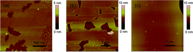 | ||
| Fig. 4 AFM images of the ultrathin films with thicknesses of 0.9 (a), 2.1 (b) and 3.6 nm (c). | ||
The above TEM and AFM results and analyses indicate that the silicon films formed on the [BMIM][BF4] surface exhibit a Stranski–Krastanov-like growth mode.25–27 First, an initial two-dimensional silicon film formed on the ionic liquid surface. Then the film grew in a layer-by-layer mode with an atomic-level smooth surface. When the thickness exceeded a critical value, three-dimensional islands and particles formed atop the silicon wetting layer uniformly and the film further thickened. In this work, the layer-plus-island growth process is mainly dependent on the surface energies and lattice parameters of the ionic liquid surface and silicon film. We have also carried out the synthesis on several kinds of ionic liquids to explore the formation mechanism of the films. Three types of results were obtained: formation of silicon films, formation of silicon and ionic liquid composite gel films and absence of any films, which means silicon particles may be produced in the bulk of the ionic liquid. We deemed preliminarily that the miscibility and wettability between silicon species and ionic liquids mainly determine the forms of silicon. In the present case, when silicon precursors encounter [BMIM][BF4], they tend to form a silicon film on the surface rather than drop into the bulk.
In summary, freestanding silicon films with the thickness ranging from 1 nm to several micrometers were prepared by Cat-CVD onto the ionic liquid surface for the first time. The non-covalent interaction between silicon species and the [BMIM][BF4] surface and their individual physical–chemical properties determine the specific film formation process. The silicon films grow in a Stranski–Krastanov-like growth mode on the [BMIM][BF4] surface and the general growth rate and crystalline structure are similar to those on a conventional solid substrate. The freestanding silicon films obtained without a solid substrate could be compatible with various device designs, which have great potential for wide applications in solar cells and optoelectronics.
Notes and references
- Thin-Film Silicon Solar Cells, ed. A. V. Shah, EFPL Press, Lausanne, 2010 Search PubMed.
- H. Águas, S. K. Ram, A. Araújo, D. Gaspar, A. Vicente, S. A. Filonovich, E. Fortunato, R. Martins and I. Ferreira, Energy Environ. Sci., 2011, 4, 4620–4632 Search PubMed.
- S. Wagner, H. Gleskova, I. C. Cheng and M. Wu, Thin Solid Films, 2003, 430, 15–19 CrossRef CAS.
- H. J. Wiesmann, US Pat., 4237150, 1980.
- H. Matsumura, H. Ihara and H. Tachibana, Proc. 18th IEEE Photovoltaic Specialists Conf., Las Vegas, 1985 Search PubMed.
- A. H. Mahan, Sol. Energy Mater. Sol. Cells, 2003, 78, 299–327 CrossRef CAS.
- H. Matsumura and K. Ohdaira, Thin Solid Films, 2009, 517, 3420–3423 CrossRef CAS.
- T. Welton, Chem. Rev., 1999, 99, 2071–2083 CrossRef CAS.
- R. D. Rogers and K. R. Seddon, Science, 2003, 302, 792–793 CrossRef.
- J. Dupont and J. D. Scholten, Chem. Soc. Rev., 2010, 39, 1780–1804 RSC.
- T. Torimoto, T. Tsuda, K. I. Okazaki and S. Kuwabata, Adv. Mater., 2010, 22, 1196–1221 CrossRef CAS.
- J. P. Hallett and T. Welton, Chem. Rev., 2011, 111, 3508–3576 CrossRef CAS.
- J. Dupont, Acc. Chem. Res., 2011, 44, 1223–1231 CrossRef CAS.
- J. J. Finley, WO Pat., 2007084558, 2007.
- T. Torimoto, K. I. Okazaki and T. Kiyama, Appl. Phys. Lett., 2006, 89, 243117 CrossRef.
- K. I. Okazaki, T. Kiyama, K. Hirahara, N. Tanaka, S. Kuwabata and T. Torimoto, Chem. Commun., 2008, 691–693 RSC.
- S. Kuwabata, T. Tsuda and T. Torimoto, J. Phys. Chem. Lett., 2010, 1, 3177–3188 CrossRef CAS.
- K. Richter, A. Birkner and A. V. Mudring, Angew. Chem., Int. Ed., 2010, 49, 2431–2435 CrossRef CAS.
- T. Suzuki, K. I. Okazaki, S. Suzuki, T. Shibayama, S. Kuwabata and T. Torimoto, Chem. Mater., 2010, 22, 5209–5215 CrossRef CAS.
- H. Wender, L. F. de Oliveira, P. Migowski, A. F. Feil, E. Lissner, M. H. G. Prechtl, S. R. Teixeira and J. Dupont, J. Phys. Chem. C, 2010, 114, 11764–11768 CAS.
- E. F. Borra, O. Seddiki, R. Angel, D. Eisenstein, P. Hickson, K. R. Seddon and S. P. Worden, Nature, 2007, 447, 979–981 CrossRef CAS.
- R. Angel, S. P. Worden, E. F. Borra, D. J. Eisenstein, B. Foing, P. Hickson, J. L. Josset, K. B. Ma, O. Seddiki, S. Sivanandam, S. Thibault and P. van Susante, Astrophys. J., 2008, 680, 1582–1594 CrossRef CAS.
- B. Yang, R. R. Ma, D. M. Li, A. G. Xia and X. M. Tao, Thin Solid Films, 2012, 520, 2321–2325 CrossRef CAS.
- S. Cheng, H. Gao, T. Ren, P. Ying and C. Li, Thin Solid Films, 2012, 520, 5155–5160 CrossRef CAS.
- J. A. Venables, G. D. T. Spiller and M. Hanbücken, Rep. Prog. Phys., 1984, 47, 399–459 CrossRef.
- D. Jing, B. Ünal, F. Qin, C. Yuen, J. W. Evans, C. J. Jenks, D. J. Sordelet and P. A. Thiel, Thin Solid Films, 2009, 517, 6486–6492 CrossRef CAS.
- A. Baskaran and P. Smereka, J. Appl. Phys., 2012, 111, 044321 CrossRef.
Footnote |
| † Electronic supplementary information (ESI) available. See DOI: 10.1039/c2ta00503d |
| This journal is © The Royal Society of Chemistry 2013 |