DOI:
10.1039/C3SM27944H
(Paper)
Soft Matter, 2013,
9, 4900-4910
Dielectrophoretic deformation of thin liquid films induced by surface charge patterns on dielectric substrates
Received
24th December 2012
, Accepted 19th March 2013
First published on 8th April 2013
Abstract
We studied the deformation of thin liquid films induced by surface charge patterns at the solid–liquid interface quantitatively by experiments and numerical simulations. We deposited a surface charge distribution on dielectric substrates by applying potential differences between a conductive liquid droplet and a grounded metal plate underneath the substrate that was moved in a pre-defined trajectory. Subsequently, we coated a thin liquid film on the substrate and measured the film thickness profile as a function of time by interference microscopy. We developed a numerical model based on the lubrication approximation and an electrohydrodynamic model for a perfect dielectric liquid. We compared experiments and simulations of the film deformation as a function of time for different charge distributions and a good agreement was obtained. Furthermore, we investigated the influence of the width of the surface charge distribution and the initial film thickness on the dielectrophoretic deformation of the liquid film. We performed a scaling analysis of the experimental and numerical results and derived a self-similar solution describing the dynamics in the case of narrow charge distributions.
I Introduction
Local build-up of electrostatic charges can potentially cause hazards, especially in high-speed processing of dielectric materials. Examples are dust attraction on solar cells1 or explosions due to charge build-up in the oil industry.2 In roll-to-roll liquid coating processes, non-uniform static charge densities at the substrate may cause deformations and defects in the final coating, whereas uniform charges are sometimes utilized to improve the coatability of partially wetting substrates.3–5
It is well known that liquid films can deform due to an inhomogeneous electric field.6 Hatfield7 recognized the application potential of this mechanism for separation processes, which since then has found numerous applications in microbiology and colloid science and technology.8,9 Chou et al. studied lithographically induced self-assembly of periodic polymer micropillar arrays10–13 and achieved feature sizes on the order of 50 nm.14 They hypothesized that the film deformations were governed by an electrohydrodynamic mechanism. Schäffer et al. studied the pattern formation and replication in ultrathin polymer films and bilayers induced by an electric field applied perpendicular to the polymer films.15–17 Subsequently, many groups conducted experiments or numerical simulations of instabilities of single or multiple liquid layers sandwiched between two electrodes kept at constant potentials.18–44 Dielectric, leaky dielectric18–20 and conductive materials45–48 were considered. Brown et al. investigated the electrostatic deformation of decanol films on interdigitated electrodes for potential use as voltage-programmable phase gratings.49,50
In contrast to voltage-controlled dielectrophoresis, much less work has been published on thin film deformation controlled by static surface charges. Miccio et al. developed a technique for thickness modulation of silicone oil films utilizing laser light induced charge patterns in photorefractive lithium niobate crystals.51 Recently, Zhao et al. used a stamping technique to create charge patterns that modulate the dewetting patterns observed after thermal annealing of ultrathin polymer layers.52 Earlier, Chudleigh53 and Engelbrecht54 created charge patterns on polymer surfaces by applying a voltage across an electrically insulating substrate through a conductive liquid for electret charging.55 Lyuksyutov et al.56,57 and Xie et al.58,59 created nanoscale surface structures in a polymer film by atomic force microscopy (AFM) with conductive tips. A salient feature of this mechanism is the electric field induced condensation of a water meniscus between the AFM tip and the polymer surface.60
In this study, we conducted a comprehensive and quantitative investigation of the deformation of low viscosity perfectly dielectric liquid films deposited on electrically insulating substrates with static surface charge patterns. We generated the charge patterns by moving an ultrapure water droplet attached to a hollow metallic needle maintained at high voltage along a dielectric substrate53,54 and characterized the obtained surface charge patterns using an electrostatic voltmeter.61 Subsequently, we deposited a thin dielectric liquid film by spin-coating and studied its deformation dynamics by interference microscopy. The results were compared to numerical simulations based on the lubrication approximation for a perfect dielectric liquid. Moreover, we performed a scaling analysis of the experimental and numerical results and derived a novel self-similar solution describing the dynamics in the case of narrow charge distributions.
II Experiments
A Surface charge deposition
We deposited electrostatic surface charge patterns on dielectric substrates by applying a voltage to a droplet of de-ionized water that was moved in a pre-defined trajectory over the dielectric substrate. Before applying the charge pattern, we de-charged the substrate using an antistatic bar (Simco-Ion MEB), which left residual charge densities of less than 2 μC m−2 on the surface. The substrates were optical quality polycarbonate plates (Bayer, Makrofol DE1-1) of thickness dsub = 750 μm. Fig. 1(a) shows a schematic of the setup. A de-ionized water droplet (Smart2Pure, TKA, resistivity 18.2 MΩ cm) was supplied from a disposable syringe (BD Plastipak 3 ml) through a polyethylene tube (Braun, Original-Perfusor Line) to a hollow metal needle (brass or stainless steel) that was connected to a high voltage DC power supply (Fug Elektronik, HCN-12500). The substrate was moved with respect to the droplet by a motorized xy-translation stage (Standa, 8MTF) that was equipped with a grounded aluminium plate for supporting the substrates and positioned underneath the stationary needle. The substrate speed Usub = 1–10 mm s−1 was low enough to avoid water loss by viscous entrainment. This process left a surface charge density along the trajectory of the droplet with a magnitude in direct correlation with the voltage Vneedle supplied to the hollow needle. The width of the charged lines W was close to the droplet size that was mainly defined by the outer diameter of the needle, Dneedle, to which the droplet was attached. The distance between the needle and the substrate was maintained at approximately 0.5 mm. We measured no change in charge patterns within hours after deposition. Synchronized control of the translation stages and high voltage power supply as well as acquisition of the signal from the electrostatic voltmeter described in Section II B was achieved by the Labview software (National Instruments).
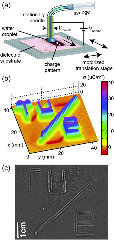 |
| | Fig. 1 (a) Schematic of the experimental setup for deposition of surface charge patterns on dielectric substrates. A droplet of water is attached to a hollow metal needle maintained at a voltage Vneedle and moved along the substrate in a pre-determined trajectory using a motorized translation stage. (b) Surface charge pattern σ(x,y), resembling a TU/e logo, as measured with an electrostatic voltmeter. (c) Photograph of the dielectrophoretic deformation of a thin liquid film of squalane, approximately 1 min after spin-coating onto the pattern of (b). | |
B Charge pattern characterization
The distribution of charges on the substrate was measured by placing the substrate on the grounded sample holder on the xy-stage described above and scanning the substrate with an electrostatic voltmeter (Monroe Electronics Isoprobe 244) equipped with a high resolution probe (Isoprobe 1017AEH) at a probe-sample distance of approximately 0.5 mm. The lateral resolution of this method is estimated62 to be approximately 0.5–1 mm, depending on the probe–surface distance (see Appendix A.1). The net surface charge density σ was calculated from the bias voltage Vbias according to61where εsub is the relative dielectric permittivity of the substrate (εsub = 2.9 for polycarbonate) and dsub is the substrate thickness. Fig. 1(b) shows a two-dimensional surface charge distribution σ(x,y) in the shape of a TU/e logo using a needle of Dneedle = 1.3 mm diameter at a voltage of Vneedle = 1250 V. Between the letters the voltage to the hollow needle was switched off. Because of the scanning movement in the y-direction with a pitch in the x-direction of 1 mm, the oblique stripe in the logo appears corrugated.
C Thin liquid film preparation and imaging
After the creation of a static charge pattern and its quantification, a thin liquid film of squalane (purity 99%, Aldrich, product number 234311) was spin-coated onto the substrate with a resulting film thickness of h0 = 4.1 μm. Squalane was selected due to its low volatility and the very low mobility of charge carriers in alkanes.63–66 The viscosity at 23 °C is μ = 31.9 mPa s, the surface tension67γ = 31.0 mN m−1, the density68ρ = 805 kg m−3 and the refractive index is n = 1.452. Within 30 s after spin-coating, the sample was removed from the spin-coater and placed in the microscope (Olympus BX51) equipped with a microscope objective (Olympus, MplanAPO 2.5×/0.04) and a CCD camera (Pike, Allied Vision Technologies) and interferometric imaging was started. During imaging, the sample was supported by a grounded and anodized aluminium plate, as sketched in Fig. 2. At a distance Htot − dsub = 0.75 mm above the sample a glass window was placed. The glass plate was coated with an electrically conductive and optically transparent indium tin oxide (ITO) layer maintained at grounded potential. This ensured that the electric potential in the system was well defined. We used an illumination setup based on a light emitting diode (Thorlabs, product number LEDC45) with a center wavelength of λ = 660 nm and a spectral width of approximately Δλ = 30 nm. By analyzing the interference fringe pattern, a cross-section of the height profile h(x) was obtained. Neighboring light and dark fringes represent height differences of λ/4n = 114 nm.
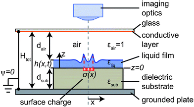 |
| | Fig. 2 Sketch of the experimental setup for characterisation of dielectrophoretic liquid film deformation, induced by the surface charge distribution σ(x) deposited on a dielectric substrate of thickness dsub. The film height profile h(x,t) was measured by interference microscopy through an ITO-coated glass plate. The bottom plate and the ITO layer were grounded, i.e. the potential ψ vanished at z = −dsub and z = Htot − dsub, respectively. | |
III Numerical model
In a long-wave approximation, the height evolution h(x,t) of a nonvolatile liquid film on a solid substrate is given by the lubrication approximation69| |  | (2) |
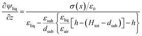
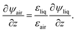
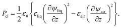
where μ is the viscosity and the augmented pressure | |  | (3) |
consists of capillary pressure, hydrostatic pressure and an electrical contribution Pel. We solved eqn (2) and (3) on a one-dimensional domain with boundary conditions| | 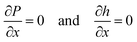 | (4) |
at x = 0 and the outer domain boundary.
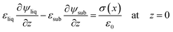
We consider one-dimensional surface charge distributions σ(x) located at the solid–liquid interface. We assume the material system to be non-conductive and without bulk charge density ρc = 0 and the relative dielectric permittivities of the liquid εliq and the solid εsub are constant and uniform. Consistent with the lubrication approximation for liquid film dynamics, the two-dimensional Poisson equation for electrostatics
| |  | (5) |
reduces to the one dimensional Laplace equation
| |  | (6) |
Therefore, the electrical potential
ψ is piecewise linear, such that
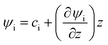
. We define the location of
z = 0 at the solid–liquid interface. The vertical positions where the potential vanishes (
ψ = 0) are therefore at the bottom plate
z = −
dsub and at the conductive glass plate
z =
Htot −
dsub =
dair +
h(
x,
t). By using the material parameters and geometrical dimensions of the experimental setup introduced in
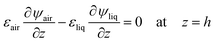
Fig. 2 and the following electrical boundary conditions
| | | ψair = 0 at z = Htot − dsub | (8) |
| |  | (11) |
| |  | (12) |
we obtain
| |  | (13) |
and
| |  | (14) |
The additional pressure Pel in the liquid film induced by the electrostatic field is determined by the Maxwell stress tensor at the liquid–air interface26,28,70
| |  | (15) |
We solved eqn (2), (3) and (13)–(15) using the finite element software COMSOL 3.5a. The width of the computational domain was 6–20 mm and the typical mesh size was 10 μm.
IV Results and discussion
A Writing of surface charges
We deposited surface charge distributions in the form of straight line segments using needles with a diameter Dneedle of 1.8 and 6 mm. The droplet followed a meandering trajectory over the substrate, during which the needle voltage Vneedle was switched on and off. A typical two-dimensional measurement of the surface charge distribution consisting of several line segments of approximately 1 cm in length is shown in Fig. 3(a). The white arrows indicate the trajectory followed during surface charge deposition, the needle voltage ranged from 313 to 2500 V. In Fig. 3(b)–(i), several cross-sections of the charge distribution have been plotted, which were obtained using needles of different diameters and different voltages and averaged over a y-interval of 7 mm. The dashed lines in Fig. 3(k) illustrate examples of such cross-sections. The resulting maximum values in this measurement series ranged from approximately 5 to 82 μC m−2. For comparison, a charge density of 50 μC m−2 corresponds to about 300 elementary charges per μm2, which indicates that our continuum lubrication description is appropriate.
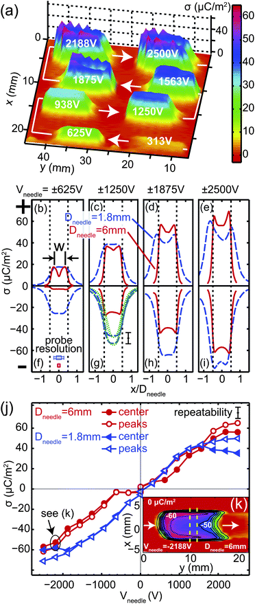 |
| | Fig. 3 Characterisation of charge density patterns deposited by the method depicted in Fig. 1. (a) Three dimensional plot of the surface charge distribution created with Dneedle = 1.8 mm and Usub = 2.5 mm s−1. The white arrows indicate the droplet trajectory, the voltage Vneedle ranged from 313 to 2500 V. (b–i) Examples of averaged cross-sections of measured charge density profiles σ(x/Dneedle) for positive (b–e) and negative (f–i) values of Vneedle. The dashed and solid lines represent experiments with Dneedle = 1.8 and 6 mm, respectively. (j) Center and peak values of σ(x) as a function of needle voltage Vneedle. (k) Contour plot of σ(x,y) of a charged line segment (Dneedle = 6 mm and Vneedle = −2188 V). The arrows represent the direction of needle movement. The vertical dashed lines illustrate typical cross-sections used to obtain an average profile similar to those in (b)–(i). | |
The influence of needle voltage on the center and peak heights of the surface charge density is plotted in Fig. 3(j). The charge density near the edges of the line, σ(±Dneedle/2), is typically higher than at the center, σ(0). The measured shape of the surface charge distribution is broadened due to the limited lateral resolution of the electrostatic voltmeter of 0.5–1 mm. Variations in the peak-to-center contrast σ(±Dneedle/2)/σ(0) are likely due to slight variation in probe-to-surface distance (see Appendix). The measured peak values monotonically increase with Vneedle. The dashed lines in Fig. 3(g) represent two independent measurements at Usub = 2.5 mm s−1 and illustrate the repeatability as indicated by the error bar. The dotted lines correspond to experiments performed with different writing speeds in the range of Usub = 1–10 mm s−1. Within repeatability, the deposited charge density is independent of Usub.
Fig. 3(k) shows a contour plot of a line segment written with Dneedle = 6 mm at a voltage Vneedle = −2188 V and substrate speed Usub = 2.5 mm s−1. The white arrows indicate the droplet trajectory. A pronounced asymmetry is observed with respect to the writing direction, which indicates that charge deposition primarily occurs at the receding contact line of the droplet, consistent with the findings of Engelbrecht.54
There are many possible mechanisms for charge transfer at a liquid–solid interface. Primarily in soft polymeric substrates like poly(dimethylsiloxane) or polyethylene,71–73 the application of a high voltage leads to the formation of ‘water-trees’, i.e. the invasion of the liquid into the polymer matrix and a permanent modification of the bulk composition and morphology. Guzenkov and Klimovich74 studied triboelectric charge generation at liquid–solid interfaces, suggesting that friction plays a role. Nakayama75 studied triboplasma generation between a diamond tip and an oil-lubricated sapphire disk. In the context of electrowetting, Vallet et al.76 observed a gas discharge in the vicinity of the contact line of electrolyte droplets. Other groups77–80 observed contact angle saturation and attributed it to charges trapped in the surface layer of the polymer. Drygiannakis et al. developed a phenomenological model based on the local breakdown of the insulating layer around the contact line.81 Koopal82 recently reviewed charging effects at solid–liquid interfaces. Using molecular dynamics simulations Liu et al. found that contact angle saturation occurs when the peak electric force near the edge of the drop exceeds the molecular binding force.83 Knorr et al.60 performed experiments of charge injection from sharp conducting needles into amorphous polymer layers. They interpreted their results as injection and surface-near accumulation of aqueous ions stemming from field-induced condensation of a water meniscus between the AFM tip and the polymer surface. Such an accumulation of trapped space charge in polymer dielectrics had been observed earlier by Wintle84 and Hibma and Zeller.85 Chudleigh considered the deposition of ions from the electric double layer at the receding contact line.53 The higher density of surface charges deposited in our experiments at x = ±W/2 is related to the fact that the electric field strength has a maximum around the contact line of the droplet,76,86 which leaves higher electrostatic charge in that region, possibly enhanced by field-induced ion dissociation.87 Hibma and Zeller85 observed injection current transients with a time constant far below 1 ms, which may explain why we do not see a significant dependence on droplet speed for Usub ≤ 10 mm s−1.
B Dielectrophoretic deformation of thin liquid films
After deposition and characterisation of the surface charge density, we applied a thin liquid film of squalane on the sample by spin-coating. We monitored the evolution of the height profile of the liquid film by interference microscopy. An example of an interference picture is shown in Fig. 4(a). The time evolution of the cross-section through the fringe pattern indicated by the dashed black line in Fig. 4(a) is visualized in Fig. 4(b). Local maxima develop at x = ±W/2, i.e. the edges of the charged line and film thickness depressions (minima) form at x ≈ ±W, which deepen and widen in time. Fig. 4(c) shows height profiles determined from the microscope images through fringe analysis. In this example, the center line film thickness hcenter = h(x = 0,t) becomes smaller during the first 200 s and thereafter increases again.
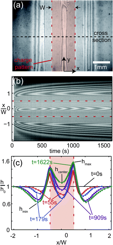 |
| | Fig. 4 Deformation of a thin dielectric liquid film due to the static surface charge distribution plotted as a dashed line in Fig. 3(b). (a) Typical interference micrograph of a thin liquid film of thickness h0 = 4.1 μm, deformed due to the presence of a straight line of surface charge, recorded at t = 118 s after film preparation. (b) Time evolution of the cross-section indicated by the dashed black line in (a). (c) Extracted film thickness profiles at different times. | |
C Influence of surface charge profile σ(x)
The actual shape of the charge density σ(x) determines the evolution of the liquid film profile h(x,t). Because of the limited lateral resolution of the measurement probe, we investigate the influence of the charge distribution on the film deformation numerically. Fig. 5(c) and (d) show a quantitative comparison of height profiles extracted from the experimental results of Fig. 4(b) at t = 300 s with numerical simulations corresponding to two different surface charge profiles σ(x), plotted in Fig. 5(a) and (b). The symbols in Fig. 5(a) and (b) correspond to the raw data of the surface charge measurements. The lines represent analytical functions σ1(x) and σ2(x), used as input for the numerical simulations. Detailed information on σ1 and σ2 is given in Appendix A.2. The charge distribution σ1(x) is chosen to faithfully represent the charge measurement data, whereas σ2(x) exhibits a pronounced maximum at the edge of the line x = ±W/2, corresponding to the observations described in Section IV A. The height and width of this maximum can be varied – though not independently – without changing the resulting deformation of the liquid film significantly. Fig. 5(b), (d) and (f) contain multiple solid lines, according to the sets of values specified in Appendix A.2. In principle one could identify the realistic combination by monitoring for instance Δhmax at very early times (10–100 ms), which however is outside the range of accessible times for our experiments. Consequently, given our experimental restrictions and reproducibility we cannot distinguish between these parameter settings. The symbols in Fig. 5(c) and (d) correspond to the experimental data, whereas the solid lines represent the numerically determined film height profiles at t = 300 s. Fig. 5(e) and (f) present the time evolution of the maximum, minimum and center line film thickness, defined in Fig. 4(c). The symbols represent experimental data and the lines represent numerical simulations. Fig. 5(g) shows the numerical simulations of Fig. 5(b), (d) and (f), visualized as an interference pattern using the procedure described in Appendix A.3 for direct comparison with Fig. 4(b). The surface charge distribution σ1 results in a simulated height profile that is in poor agreement with the measured profile in Fig. 5(c). The amplitude of deformation is much lower than experimentally observed; the center height is too high, the peak amplitude is too low and the minimum is not deep enough. The agreement remains comparably poor for different times, as shown in Fig. 5(e). The experimental center film thickness hcenter shows an initial decrease, whereas the simulated value increases monotonically. In contrast, the surface charge distribution σ2(x) results in excellent agreement between the experimental and numerical film height profiles, not only at t = 300 s [Fig. 5(d)] but also over the entire time interval considered in Fig. 5(f). The simulated center film thickness now reproduces the experimentally observed local minimum at t ≈ 200 s. The occurrence of this minimum, i.e. the initial decrease of the center line thickness, is primarily due to the positive charge density gradient towards the peaks at x = ±W/2. This induces a flow away from the center until a decrease in capillary pressure reverses the trend.
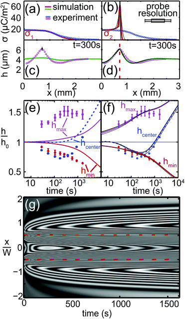 |
| | Fig. 5 Comparison of measured (symbols) and simulated liquid film height profiles at t = 300 s (c and d) for different surface charge distributions, sketched in (a) and (b). The solid lines in (a) and (b) represent the surface charge distributions used as an input to the simulations. The solid lines in (c) and (d) are the simulations results. (e and f) Normalized film thickness as a function of time. The squares refer to the maximum value at x = ±W/2; the diamonds refer to the valley at x ≈ ±W and the circles refer to the film thickness at position x = 0. The solid and dashed lines refer to the numerical simulations. (g) Numerical simulations of (b), (d) and (f), visualized as an interference pattern for direct comparison with Fig. 4(b). | |
Fig. 6 presents experimental and numerical results of the time evolution of key features in the film thickness profile for charge distributions of different magnitude. For the numerical simulations, the surface charge profile σ2 shown in Fig. 5(b) was scaled proportional to the center values of the charge density distribution plotted as solid triangles in Fig. 3(j). Fig. 6(a)–(c) show the normalized change in film thickness Δh/h0 ≡ (h/h0) − 1 of the maximum at x = ±W/2, the minimum at x ≈ W and the center at x = 0. In Fig. 6(d), we plot the position of the outer minimum relative to the edge of the charged line (x = ±W/2) as a function of time for different magnitudes of surface charge density. The dashed black line corresponds to a power law of 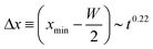 .
.
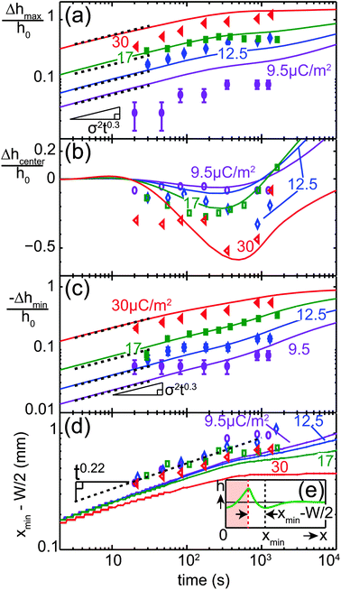 |
| | Fig. 6 Time evolution of the normalized change in film thickness Δh(x,t) for different surface charge densities. Normalized change in film thickness (a) at the maxima (x = ±W/2), (b) in the center (x = 0) and (c) in the local minimum next to the charged line. (d) Relative distance between the film thickness minimum and the edges of the line at x = W/2 as a function of time. The dashed black line corresponds to a power law Δx ∼ t0.22. (e) Example of a film thickness profile h(x) illustrating the distance xmin − W/2, plotted in (d). The symbols and solid lines represent the experimental data and numerical results, respectively. | |
The simulations reproduce the trend in the experimental data very well, but the exact numerical values of the deformation are not captured accurately. According to eqn (13)–(15), Pel scales as σ2, which amplifies the experimental uncertainty associated with measurements of σ(x) as discussed in the context of Fig. 3(g). Moreover, the charge distribution may not only change in magnitude proportional to needle voltage, but also somewhat in shape. The depths of the center hcenter and outer minima hmin generally agree better with the simulations than the maximum values. This indicates that the uncertainty in the charge distributions σ(x) is predominant in the vicinity of the peak values in σ(x). Within reproducibility, the experimental data in Fig. 6(d) do not show any dependence on charge density σ. The numerical curve for σ = 30 μC m−2 apparently saturates at t ≈ 1000 s, roughly coinciding with the time at which −Δhmin approaches its maximum possible value, h0, i.e. hmin → 0 in Fig. 6(c).
D Influence of initial film thickness h0 and line width W
The comparison between experiments and simulations, presented in the previous subsection, constitutes a general validation of the numerical model. In the following sections, we study the influence of different geometric parameters on the thin film evolution by numerical simulations. Fig. 7(a)–(c) show the influence of the initial film thickness h0 on the normalized change in the film thickness of the maximum at x = ±W/2, the minimum at x ≈ W and the center at x = 0. At early times t < 1 s, the rate of deformation increases with film thickness. From t ≳ 50 s the curves for different values of h0 in Fig. 7(a) and (c) essentially collapse. For early times, the development of the maximum and minimum height follows a linear time dependence, as indicated by the dashed black lines. The center line height Δhcenter(t)/h0 exhibits a local minimum in time, which occurs earlier but becomes shallower for higher film thickness h0.
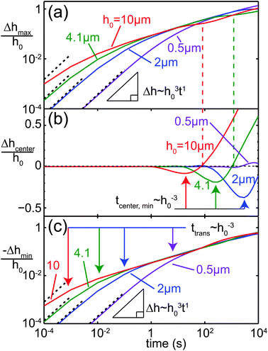 |
| | Fig. 7 Influence of initial film thickness h0 on film deformation Δh(x,t). Normalized change in film thickness (a) at the maximum (x = W/2), (b) at the center (x = 0) and (c) at the local minimum next to the charged line. The dashed black lines in (a) and (c) represent power laws of exponent 1. The arrows in (b) and (c) indicate power law behavior tmin ∼ h0−3 for the time at which the center film thickness assumes its minimum value and ttrans ∼ h0−3 for the transition time defined in Section IV E. | |
The influence of the line width W is illustrated in Fig. 8. Fig. 8(a) and (b) show the time evolution of the height profile for two values of W = 0.4 and 4 mm. In Fig. 8(c)–(e), the influence of W on the normalized change in the film thickness of the maximum at x = ±W/2, the minimum outside the charged line and the center at x = 0 is shown. For small values of W, the two maxima at x = ±W/2 observed at early times merge into a single peak due to the negative capillary pressure caused by the close proximity of the peaks. For wider lines, the two peaks remain for the entire simulated time interval. The center line height Δhcenter(t)/h0 exhibits a local minimum in time, which occurs later and becomes deeper for larger W. The times at which the local minima occur in Fig. 7(b) and 8(d) correspond to power laws tmin ∼ h0−3 and ∼W3.8, respectively, as indicated by the arrows in Fig. 7(b) and 8(d).
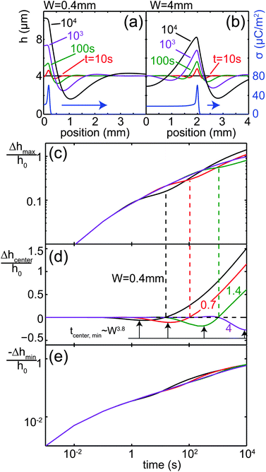 |
| | Fig. 8 Influence of line width W on Δh(x,t). (a) Film profiles at different points in time for (a) W = 0.4 mm and (b) W = 4 mm. (c) Film thickness at the maxima x = ±W/2. (d) Center line film thickness at x = 0. The arrows indicate power law behavior for the time at which the local minimum occurs. (e) Film thickness in the minimum next to the charged line. | |
E Scaling analysis and self-similar solutions
In the early phase, the height profile h = h0 + Δh, where Δh ≪ h0, deviates very little from the prescribed initial condition h = h0, which allows linearization of the lubrication equation. Moreover, the electrical pressure Pel ∼ σ2(x) is almost independent of Δh and the capillary and hydrostatic contributions are negligible. Consequently, an approximate solution to the lubrication equation is given by Δh ∼ h03f′′(x)t, which is represented by the dashed lines in Fig. 7(a). Here, f(x) ≡ σ2(x).
Motivated by the presence of sharp peaks of the charge density at the line edges, we now consider an infinitely narrow electrical pressure distribution
where the function
F(
h) is determined by
eqn (13)–(15) and we introduce the following non-dimensional quantities
| | ![[h with combining macron]](https://www.rsc.org/images/entities/i_char_0068_0304.gif) = h/h0, = h/h0, ![[x with combining macron]](https://www.rsc.org/images/entities/i_char_0078_0304.gif) = x/W = x/W | (17) |
| |  | (18) |
For a uniform initial condition
h(
t = 0) =
h0 or equivalently
(
![[t with combining macron]](https://www.rsc.org/images/entities/i_char_0074_0304.gif)
= 0) = 1, the hydrostatic pressure contribution is negligible initially, until the resulting film thickness perturbation spreads much further than the capillary length

. Consequently, in this regime the non-dimensionalization of
eqn (2) and
(3) results in
| |  | (19) |
where we defined
![[P with combining macron]](https://www.rsc.org/images/entities/i_char_0050_0304.gif) el
el ≡
W2Pel/(
γh0). We consider small perturbations
= 1 +
1, where
1 ≡ Δ
h/
h0 ≪ 1, which yields a linearized lubrication equation
| | 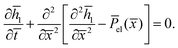 | (20) |
We seek a self-similar solution for the function
φ ≡
1/
β in the reduced coordinate
η≡
/
α, which results in
| | 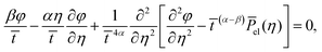 | (21) |
where we made use of the scaling property of the delta function
| | 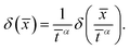 | (22) |
Consequently, a self-similar solution exists for the exponents
α =
β = 1/4 with the corresponding ordinary differential equation
| | 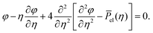 | (23) |
Fig. 9 shows solutions of
eqn (2) and
(3) represented in terms of the non-dimensional film deformation
φ(
η) for nine points in time and a delta-like charge distribution
σ3 (see Appendix). The nine curves, corresponding to eight decades in time, essentially collapse as expected from the self-similar solution. The shape of the curves qualitatively resembles the experimental and numerical solution depicted in
Fig. 5(d).
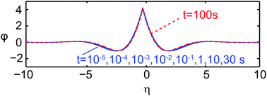 |
| | Fig. 9 Nine numerical solutions of eqn (2) and (3) represented in terms of the non-dimensional film deformation φ(η) for eight decades in time and a delta-like charge distribution σ3 (h0 = 4.1 μm and W = 1.4 mm). | |
In view of this self-similar solution, one would expect power law relationships tmin ∼ h0−3W4 in Fig. 7(b) and 8(d), which is in excellent agreement with the observed scaling behavior. These scalings coincide with those of capillary redistribution dynamics,88,89 because there is only a relatively small variation in σ between the peak positions |x| < W/2 and away from the charged line |x| > W/2.
The dashed line in Fig. 6(d) corresponds to a power law with exponent 0.22, which is close to the value of 1/4, that is also expected for capillary redistribution in thin liquid films90 in the regime Δh/h0 ≪ 1. Since the non-dimensional deformation Δh/h0 for the data corresponding to σ = 30 μC m−2 approaches one, the agreement is better for smaller values of σ. The dashed lines in Fig. 6(a) and (c) correspond to power laws Δhmax ∼ t0.3. The reasons for the slight deviation from the exponent 0.25 expected from the self-similar solution are that the condition Δh ≪ h0 is not perfectly fulfilled in all cases, that the influence of the transition from the linear regime still lingers on and that the two interior minima in the region |x| < W/2 begin to merge at t ≈ 10 s.
For our case of a peak in the charge distribution that has a small – but finite – width wpeak, the transition between the linear regime Δh ∼ t and the self-similar regime  can be estimated to occur when the width of the self-similar solution exceeds wpeak. According to the definition of the reduced coordinate η = /α, we expect the transition time to scale as ttrans ∼ 3μwpeak4/(γh03), i.e. to be independent of W, which is consistent with Fig. 7(c) and 8(e).
V Summary
We investigated the impact of static surface charge distributions on the deformation of thin films of a dielectric liquid on a solid substrate by means of experiments and numerical simulations. We deposited patterns of surface charges by dragging a droplet over the substrate in a pre-defined trajectory, while attached to a needle, maintained at high voltage. We measured the surface charge distribution using an electrostatic voltmeter and characterized the charge density profile as a function of the needle voltage and diameter. Subsequently, we spin-coated a thin film of a dielectric liquid onto the charged substrate and measured the time evolution of the film thickness distribution by interference microscopy. We obtained good agreement between experiments and numerical simulations based on the lubrication approximation and a dielectrophoretic pressure. We systematically investigated the influence of the charged line width, initial film thickness and surface charge magnitude and elucidated the observed scaling behavior by means of a self-similar solution.
Appendix A
1 Influence of probe-to-surface distance
Fig. 10 shows several measurements of the same surface charge density profile σ(x), scanned at different distances H between the charged substrate and electrostatic voltmeter probe. The charge was deposited using a needle of diameter Dneedle = 6 mm at a voltage Dneedle = −1250 V. The peaks at the edges of the charge distribution, x = ± W/2, are more pronounced in measurements with smaller probe-to-surface distance.
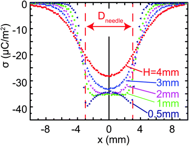 |
| | Fig. 10 Influence of the probe to substrate distance on the measured charge density profile σ(x). | |
2 Expressions for charge distributions σ(x)
The analytical expression for the charge distribution σ1(x) presented in Fig. 5(a) is| | 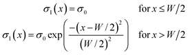 | (A.1) |
with W = 1.4 mm and σ0 = 17 μC m−2. The analytical expression for σ2(x) as used in the simulations is| | 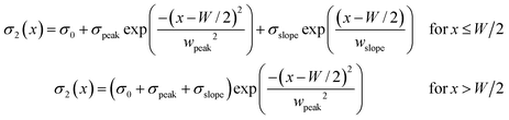 | (A.2) |
with σ0 = 17 μC m−2, wslope = 0.2 mm and σslope = 8 μC m−2 and W is a variable. For the simulations presented in the paper, the values wpeak = 50 μm and σpeak = 37 μC m−2 were used. Table 1 shows examples of alternative combinations yielding indistinguishable results.
Table 1 Combinations of wpeak and σpeak, resulting in equivalent thin film deformation results. The combinations fulfill wpeak × σpeak3/2 = (490 ± 10) μm (μC m−2)3/2
|
w
peak (μm) |
σ
peak (μC m−2) |
| 10 |
106 |
| 25 |
60 |
| 50 |
37 |
| 100 |
23 |
The analytical expression for σ3(x) as used in the simulations is
| | 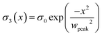 | (A.3) |
with
wpeak = 0.5 μm and
σ0 = 800 μC m
−2.
3 Interference visualization
The conversion of a film thickness profile h(x,t) to the greyscale fringe-pattern in Fig. 5(g) was achieved by using a positive periodic function C(h) with an amplitude, slowly decaying within the relevant thickness range h ≲ 8 μm.| | 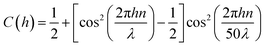 | (A.4) |
with n = 1.452 the refractive index for the liquid film of squalane and λ = 660 nm the center wavelength of the illumination light source.
Acknowledgements
This work is part of the research programme ‘Contact Line Control during Wetting and Dewetting’ (CLC) of the ‘Stichting voor Fundamenteel Onderzoek der Materie (FOM)’, which is financially supported by the ‘Nederlandse Organisatie voor Wetenschappelijk Onderzoek (NWO)’. The CLC programme is co-financed by ASML and Océ. The authors thank Hein Castelijns, Michel Riepen and Ramin Badie of ASML for providing the opportunity for Kees Kuijpers to perform experiments in the immersion lithography research laboratory. The authors thank Ellen Moons and Andrzej Dzwilewski of the Physics Department of Karlstad University for welcoming Christian Berendsen to their laboratory to explore alternative surface charge characterisation techniques.
References
- M. Mani and R. Pillai, Renew. Sust. Energ. Rev., 2010, 14, 3124 CrossRef.
-
A. Klinkenberg, J. L. van der Minne and R. D. Shell, Electrostatics in the Petroleum Industry: The Prevention of Explosion Hazards, Elsevier Publishing Company, 1958 Search PubMed.
-
E. D. Cohen and E. B. Gutoff, Modern Coating and Drying Technology, VCH, New York, 1992 Search PubMed.
-
G. F. Nadeau, Method of coating a liquid photographic emulsion on the surface of a support, US Pat., 2,952,559, 1960.
- T. D. Blake, A. Clarke and E. Stattersfield, Langmuir, 2000, 16, 2928 CrossRef CAS.
- J. Swan, Proc. R. Soc. London, 1897, 62, 38 CrossRef.
-
H. Hatfield, Means and process of separating substances one from another, US Pat., 1,498,911, 1924.
-
H. A. Pohl, Dielectrophoresis: The Behavior of Neutral Matter in Nonuniform Electric Fields, Cambridge University Press, Cambridge, 1978, vol. 80 Search PubMed.
- R. Pethig, Biomicrofluidics, 2010, 4, 022811 CrossRef.
- S. Y. Chou, L. Zhuang and L. Guo, Appl. Phys. Lett., 1999, 75, 1004 CrossRef CAS.
- S. Y. Chou and L. Zhuang, J. Vac. Sci. Technol., B, 1999, 17, 3197 CAS.
- L. Wu and S. Y. Chou, Appl. Phys. Lett., 2003, 82, 3200 CrossRef CAS.
- L. F. Pease III and W. B. Russel, J. Chem. Phys., 2006, 125, 184716 CrossRef.
- M. Li, L. Chen, W. Zhang and S. Y. Chou, Nanotechnology, 2002, 14, 33 CrossRef.
- E. Schäffer, T. Thurn-Albrecht, T. P. Russell and U. Steiner, Nature, 2000, 403, 874 CrossRef.
- E. Schäffer, T. Thurn-Albrecht, T. P. Russell and U. Steiner, Europhys. Lett., 2007, 53, 518 CrossRef.
- M. D. Morariu, N. E. Voicu, E. Schäffer, Z. Lin, T. P. Russell and U. Steiner, Nature Mater., 2003, 2, 48 CrossRef CAS.
- J. Melcher and G. Taylor, Annu. Rev. Fluid Mech., 1969, 1, 111 CrossRef.
- J. R. Melcher and C. V. Smith, Phys. Fluids, 1969, 12, 778 CrossRef.
- D. Saville, Annu. Rev. Fluid Mech., 1997, 29, 27 CrossRef.
- S. Herminghaus, Phys. Rev. Lett., 1999, 83, 2359 CrossRef CAS.
- Z. Lin, T. Kerle, T. P. Russell, E. Schäffer and U. Steiner, Macromolecules, 2002, 35, 3971 CrossRef CAS.
- Z. Lin, T. Kerle, T. P. Russell, E. Schäffer and U. Steiner, Macromolecules, 2002, 35, 6255 CrossRef CAS.
- L. F. Pease III and W. B. Russel, J. Non-Newt. Fluid Mech., 2002, 102, 233 CrossRef.
- J. Peng, Y. Han, Y. Yang and B. Li, Polymer, 2003, 44, 2379 CrossRef CAS.
- V. Shankar and A. Sharma, J. Colloid Interface Sci., 2004, 274, 294 CrossRef CAS.
- N. Wu, L. F. Pease III and W. B. Russel, Langmuir, 2005, 21, 12290 CrossRef CAS.
- R. Verma, A. Sharma, K. Kargupta and J. Bhaumik, Langmuir, 2005, 21, 3710 CrossRef CAS.
- R. Craster and O. Matar, Phys. Fluids, 2005, 17, 032104 CrossRef.
- H. K. Yeoh, Q. Xu and O. A. Basaran, Phys. Fluids, 2007, 19, 114111 CrossRef.
- F. Li, X.-Y. Yin and X.-Z. Yin, Chin. Phys. Lett., 2008, 25, 2546 CrossRef CAS.
- M. D. Dickey, A. Raines, E. Collister, R. T. Bonnecaze, S. Sreenivasan and C. G. Willson, J. Mater. Sci., 2008, 43, 117 CrossRef CAS.
- N. Wu and W. B. Russel, Nano Today, 2009, 4, 180 CrossRef CAS.
- D. Bandyopadhyay, A. Sharma, U. Thiele and P. D. S. Reddy, Langmuir, 2009, 25, 9108 CrossRef CAS.
- J. Heier, J. Groenewold and U. Steiner, Soft Matter, 2009, 5, 3997 RSC.
- S. A. Roberts and S. Kumar, J. Fluid Mech., 2009, 631, 255 CrossRef.
- P. Gambhire and R. Thaokar, Phys. Fluids, 2010, 22, 064103 CrossRef.
- P. D. S. Reddy, D. Bandyopadhyay and A. Sharma, J. Phys. Chem. C, 2010, 114, 21020 CAS.
- S. Srivastava, P. D. S. Reddy, C. Wang, D. Bandyopadhyay and A. Sharma, J. Chem. Phys., 2010, 132, 174703 CrossRef.
- A. Atta, D. G. Crawford, C. R. Koch and S. Bhattacharjee, Langmuir, 2011, 27, 12472 CrossRef CAS.
- B. Khorshidi, M. Jalaal and E. Esmaeilzadeh, Colloids Surf., A, 2011, 380, 207 CrossRef CAS.
- J. Zhang, J. Zahn and H. Lin, J. Fluid Mech., 2011, 681, 293 CrossRef.
- G. Amarandei, P. Beltrame, I. Clancy, C. O'Dwyer, A. Arshak, U. Steiner, D. Corcoran and U. Thiele, Soft Matter, 2012, 8, 6333 RSC.
- P. D. S. Reddy, D. Bandyopadhyay and A. Sharma, J. Phys. Chem. C, 2012, 116, 22847 CAS.
- S. Veremieiev, H. Thompson, M. Scholle, Y. Lee and P. Gaskell, Int. J. Multiph. Flow, 2012, 44, 48 CrossRef CAS.
- N. Zubarev, Physica D, 2001, 152, 787 CrossRef.
- D. Tseluiko and D. T. Papageorgiou, SIAM J. Appl. Math., 2007, 67, 1310 CrossRef.
- X.-F. Wu and Y. A. Dzenis, J. Phys. D: Appl. Phys., 2005, 38, 2848 CrossRef CAS.
- C. Brown, W. Al-Shabib, G. Wells, G. McHale and M. I. Newton, Appl. Phys. Lett., 2010, 97, 242904 CrossRef.
- C. Brown, G. Wells, M. Newton and G. McHale, Nature Phot., 2009, 3, 403 CrossRef CAS.
- L. Miccio, M. Paturzo, A. Finizio and P. Ferraro, Opt. Express, 2010, 18, 10947 CrossRef CAS.
- D. Zhao, A. D. Martinez, X. Xi, X. Ma, N. Wu and T. Cao, Small, 2011, 7, 2326 CrossRef CAS.
- P. Chudleigh, J. Appl. Phys., 1976, 47, 4475 CrossRef CAS.
- R. Engelbrecht, J. Appl. Phys., 1974, 45, 3421 CrossRef CAS.
-
G. Sessler and R. Gerhard-Multhaupt, Electrets, Laplacian, Morgan Hill, 1998 Search PubMed.
- S. F. Lyuksyutov, R. A. Vaia, P. B. Paramonov, S. Juhl, L. Waterhouse, R. M. Ralich, G. Sigalov and E. Sancaktar, Nature Mater., 2003, 2, 468 CrossRef CAS.
- S. F. Lyuksyutov, P. B. Paramonov, S. Juhl and R. A. Vaia, Appl. Phys. Lett., 2003, 83, 4405 CrossRef CAS.
- X. N. Xie, H. J. Chung, C. H. Sow, A. A. Bettiol and A. T. S. Wee, Adv. Mater., 2005, 17, 1386 CrossRef CAS.
- X. N. Xie, H. J. Chung, C. H. Sow, K. Adamiak and A. T. S. Wee, J. Am. Chem. Soc., 2005, 127, 15562 CrossRef CAS.
- N. Knorr, S. Rosselli, T. Miteva and G. Nelles, J. Appl. Phys., 2009, 105, 114111 CrossRef.
- C. W. Reedyk and M. M. Perlman, J. Electrochem. Soc., 1968, 115, 49 CrossRef.
-
Monroe Electronics, Datasheet Miniature Electrostatic Voltmeter Probes, Model 1017A/1034, 2002 Search PubMed.
-
I. Adamczewski, Ionisation, Conductivity and Breakdown in Dielectric Liquids, Taylor & Francis, London, 1969 Search PubMed.
-
A. O. Allen and N. Dame, Tech. Rep. NSRDS-NBS 58, US Department of Commerce, National Bureau of Standards, 1976 Search PubMed.
-
W. Schmidt, Conduction mechanisms in liquids, in Electrical Insulating Liquids, ASTM International, Philadelphia, 1994, vol. 3, p. 147 Search PubMed.
- J.-P. Jay-Gerin and C. Ferradini, J. Chem. Phys., 1990, 93, 3718 CrossRef CAS.
- M. De Ruijter, P. Kölsch, M. Voué, J. De Coninck and J. Rabe, Colloids Surf., A, 1998, 144, 235 CrossRef CAS.
- A. Kumagai and S. Takahashi, Int. J. Thermophys., 1995, 16, 773 CrossRef CAS.
- A. Oron, S. H. Davis and S. G. Bankoff, Rev. Mod. Phys., 1997, 69, 931 CrossRef CAS.
-
H. H. Woodson and J. Melcher, Electromechanical Dynamics. Part III: Elastic and Fluid Media, John Wiley & Sons Inc., New York, 1968 Search PubMed.
- J. Fothergill, A. Eccles, A. Houlgreave and L. Dissado, IEE Proc.-A: Sci., Meas. Technol., 1993, 140, 397 CrossRef CAS.
- J.-P. Crine and J. Jow, IEEE Trans. Dielectr. Electr. Insul., 2005, 12, 801 CrossRef.
- C. Stancu, P. V. Notingher, F. Ciuprina, P. Notingher, J. Castellon, S. Agnel and A. Toureille, IEEE Trans. Ind. Appl., 2009, 45, 30 CrossRef.
- S. Guzenkov and A. Klimovich, Wear, 1993, 161, 79 CrossRef CAS.
- K. Nakayama, Tribol. Lett., 2011, 41, 345 CrossRef.
- M. Vallet, M. Vallade and B. Berge, Eur. Phys. J. B, 1999, 11, 583 CrossRef CAS.
- H. Verheijen and M. Prins, Langmuir, 1999, 15, 6616 CrossRef CAS.
- F. Mugele and J.-C. Baret, J. Phys.: Condens. Matter, 2005, 17, R705 CrossRef CAS.
- B. Janocha, H. Bauser, C. Oehr, H. Brunner and W. Göpel, Langmuir, 2000, 16, 3349 CrossRef CAS.
- J. Restolho, J. L. Mata and B. Saramago, J. Phys. Chem. C, 2009, 113, 9321 CAS.
- A. I. Drygiannakis, A. G. Papathanasiou and A. G. Boudouvis, Langmuir, 2008, 25, 147 CrossRef.
- L. K. Koopal, Adv. Colloid Interface Sci., 2012, 29, 29 CrossRef.
- J. Liu, M. Wang, S. Chen and M. O. Robbins, Phys. Rev. Lett., 2012, 108, 216101 CrossRef.
- H. Wintle, J. Non-Cryst. Solids, 1974, 15, 471 CrossRef CAS.
- T. Hibma and H. Zeller, J. Appl. Phys., 1986, 59, 1614 CrossRef CAS.
- K. H. Kang, Langmuir, 2002, 18, 10318 CrossRef CAS.
- L. Onsager, J. Chem. Phys., 1934, 2, 599 CrossRef CAS.
- S. Orchard, Appl. Sci. Res., 1963, 11, 451 Search PubMed.
- L. Stillwagon and R. Larson, J. Appl. Phys., 1988, 63, 5251 CrossRef CAS.
- B. Brasjen, H. Gu and A. Darhuber, Microfluid. Nanofluid., 2013, 14, 669 CrossRef CAS.
|
| This journal is © The Royal Society of Chemistry 2013 |
Click here to see how this site uses Cookies. View our privacy policy here.  Open Access Article
 This Open Access Article is licensed under a