On chemical bonding and electronic structure of graphene–metal contacts†
Brian J.
Schultz
a,
Cherno
Jaye
b,
Patrick S.
Lysaght
c,
Daniel A.
Fischer
b,
David
Prendergast
d and
Sarbajit
Banerjee
*a
aDepartment of Chemistry, University at Buffalo, The State University of New York, Buffalo, New York 14260–3000, USA. E-mail: sb244@buffalo.edu
bMaterial Measurement Laboratory, National Institute of Standards and Technology, Gaithersburg, Maryland 20899, USA
cFront-End Process Division, SEMATECH, 2706 Montopolis Drive, Austin, Texas 78741, USA
dMolecular Foundry, Lawrence Berkeley National Laboratory, Berkeley, California, 94720 USA
First published on 2nd November 2012
Abstract
The nature of chemical bonding at graphene–metal interfaces is intriguing from a fundamental perspective and has great relevance for contacts to novel spintronics and high-frequency electronic devices. Here, we use near-edge X-ray absorption fine structure (NEXAFS) spectroscopy in conjunction with Raman spectroscopy and first-principles density functional theory to examine chemical bonding and perturbation of the π-electron cloud at graphene–metal interfaces. Graphene–metal bonding has been contrasted for graphene interfaced with single-crystalline metals, polycrystalline metal foils, and with evaporated metal overlayers and is seen to be strongest at the last noted interface. Strong covalent metal-d-graphene-π hybridization and hole doping of graphene is observed upon deposition of Ni and Co metal contacts onto graphene/SiO2 and is significantly stronger for these metals in comparison to Cu. Of single-crystalline substrates, the most commensurate (111) facets exhibit the strongest interactions with the graphene lattice. First-principles electronic structure simulations, validated by direct comparison of simulated spectra with NEXAFS measurements, suggest that metal deposition induces a loss of degeneracy between the α- and β-graphene sublattices and that spin-majority and spin-minority channels are distinctly coupled to graphene, contributing to splitting of the characteristic π* resonance. Finally, the electronic structure of graphene is found to be far less perturbed by metal deposition when the π cloud is pinned to an underlying substrate; this remarkable behaviour of “sandwich” structures has been attributed to electronic accessibility of only one face of graphene and illustrates the potential for anisotropic functionalization.
Introduction
Accurate description of chemical bonding at interfaces must necessarily encompass the complexities associated with wedding disparate materials characterized by distinct surface electronic structures, but is nonetheless imperative for rational materials design and to develop a fundamental understanding of the peculiarities of interfacial phenomena. Single-layered graphene (SLG) is a quintessential example of a material wherein interfacial phenomena assume special importance since every atom in the honeycomb-like structure resides on the surface.1–6 Herein, we examine the electronic accessibility of the two faces of graphene and use near-edge X-ray absorption fine structure (NEXAFS) spectroscopy in conjunction with density functional theory (DFT) spectral simulations to develop a comprehensive description of the nature of the chemical bond formed at graphene–metal interfaces.The remarkable transport properties of graphene are derived from the subtleties of its electronic structure, particularly the topological peculiarities at the K point of the Brillouin zone of graphene, wherein conduction bands cross the Fermi level with a linear (photon-like) energy dispersion within ±1 eV.1,2,7,8 Given the entirely surficial geometric structure of graphene, the manifestation of Dirac physics in this material is substantially modulated by perturbations of the electronic structure as a result of interactions with charged impurities, coupling to the underlying substrate, orbital hybridization with deposited contacts, and buckling/corrugation of graphene sheets.3,6,9–15 The interactions of transition metal adatoms and surfaces with graphene are particularly intriguing and of specific relevance to imparting spin polarization to the graphene Fermi surface (via the Rashba effect),13,16,17 manifestation of unusual Kondo physics and unique magnetic states,14,18 sustaining supercurrent within mesoscopic junctions,11 and for charged impurity scattering.3,6,10,19 Nevertheless, studies of chemical bonding at graphene–metal interfaces remain sparse, and theoretical predictions have substantially outpaced experimental studies of realistic graphene–metal contacts.4,19–26 As an element specific probe of the unoccupied density of states (UDOS) above the Fermi level, NEXAFS spectroscopy provides exceptional insight into electronic structure perturbations introduced at interfaces and is used here in conjunction with Raman spectroscopy to examine the electronic structure details of graphene–metal hybridized interfaces.9,10,25,27
Graphene–metal interfaces have been subjected to substantial theoretical examination with DFT calculations suggesting a bimodal distribution of bonding strengths, differentiated in the literature as physisorption and chemical hybridization regimes.20–22,24 The extent of perturbation of the electronic structure of graphene is predicted to vary as a function of the metal binding energies, the probability of metal–carbide bond formation, commensurability, and crystallographic orientation.21,23,24,28 NEXAFS spectra at the carbon K-edge are sensitive to changes in the bonding environment of graphene. The π* and σ* (∼285 and ∼292 eV) features represent, to a first approximation, a replica of the carbon p-projected UDOS just above the Fermi level.29,30 The X-ray absorption process is well approximated by a Fermi's golden rule expression, which describes the probability of exciting a core-electron from an initial ground state to an electron-occupation-constrained self-consistent final state.29–31 Here, we have used NEXAFS spectroscopy to examine the details of chemical bonding at three kinds of metal–graphene interfaces: graphene grown on single crystal metal substrates, graphene grown on polycrystalline metal foil, and graphene with evaporated overlayers of metal atoms. Distinct crystal-facet dependence of the strength of chemical bonding is observed for graphene grown on single crystal metal surfaces. The most remarkable differences in graphene–metal hybridization is evidenced upon deposition of metal overlayers including the manifestation of a hitherto unprecedented “protecting group” effect of an underlying metal substrate on the reactivity of the exposed graphene surface.
Results and discussion
We begin by examining graphene grown by thermal decomposition of CH4 gas on single crystals and foils of Cu and Ni (see ESI†). Based on DFT calculations, Cu and Ni are the two endpoints of a broad spectrum of metal adsorption classifications, wherein graphene is proposed to be chemisorbed onto Ni substrates and physisorbed onto Cu substrates.4,20,21,24,32Fig. 1a compares C K-edge NEXAFS spectra acquired for graphene grown on Cu foils at two different partial pressures of CH4 (and different cooling rates) as well as on Cu[100], Cu[110], and Cu[111] surfaces; more dramatic differences are discernible in Fig. 1b, which depicts the equivalent comparison for graphene on Ni substrates. Fig. S1 (ESI†) shows Raman spectra acquired for the corresponding samples suggesting SLG growth on Cu foil but stabilization of bilayered and few-layered graphene on the single crystalline substrates (based on the relative 2D/G intensity ratios). Some stiffening and possible lifetime broadening of phonons is noted for graphene grown on single-crystalline substrates, which could be a result of charge transfer and inhomogeneities in the pinning of the graphene to the rigid substrates. As noted above, the NEXAFS spectra are characterized by transitions to π* states, an excitonic set of σ* states, and also show resonances characteristic of adsorbates that are well-separated at ∼287 eV, assigned as such based on our previous in situ heating studies, and denoted in Fig. 1 and 2 as the intermediate region.10 The C K-edge NEXAFS spectra for graphene grown on Cu and Ni foils exhibit a distinctive broadening and splitting of the graphene π* feature.9,26 The increased spectral envelope in the π* region is discussed in more detail below with reference to ab initio calculations. However, comparison of spectra for the two graphene/Cu or graphene/Ni foil samples in Fig. 1a and b suggests that substantial variation in interfacial bonding strength can be induced by altering the reaction conditions for graphene growth on polycrystalline foil. All NEXAFS spectra are presented at 85° incidence of the X-ray beam at which the distinct “pre-edge” or low-energy shoulders to the π* resonance are most clearly distinguishable from the primary π* absorption. NEXAFS data acquired at 25° incidence of the X-ray beam are presented in Fig. S2.† One explanation for the discrepancies in π* splitting noted across Cu and Ni foil samples might be attributed to an increased height (dz), perpendicular to the metal surface, based on the specifics of the cooling rates or the subsequent oxidation of the metal surface (variations in peak positions of Raman bands are also noted); which can introduce large variations (i.e., buckling or rippling) as a result of the varying thermal expansion coefficients between graphene and the transition metal substrate. The observed variations in these spectra thus strongly suggest that graphene residing atop a metal surface on which it has been grown by thermal decomposition does not represent an ideal model system for examination of interfacial chemical bonding due to inevitable variations in dz. Fig. 2 (vide infra) depicts NEXAFS and Raman spectra of graphene with an evaporated metal overlayer that serves as an excellent model for examining graphene–metal bonding with a more pronounced splitting of the π* feature.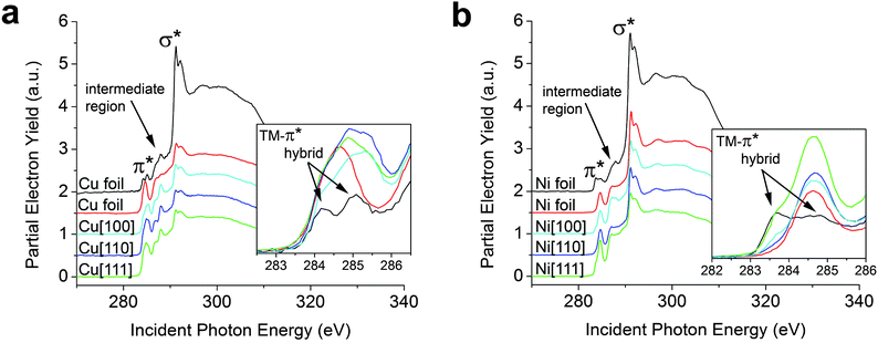 | ||
| Fig. 1 Graphene synthesized on polycrystalline and single crystal copper and nickel substrates. NEXAFS spectra have been acquired at 85° incidence of the X-ray beam for SLG and FLG on Cu and Ni substrates prepared by vapour deposition as discussed in the methods section. (a) The two Cu foil spectra are two analogous SLG samples fabricated on Cu foil—the extent of substrate hybridization is found to be sensitive to the specifics of the growth conditions, which alter the interlayer spacing. (b) The two Ni foil spectra are two analogous SLG samples fabricated on Ni foil, once again the interlayer spacing and thus the extent of substrate hybridization depends upon the specific reaction conditions. The most prominent spectral features are assigned to the transitions to final states of π* and σ* symmetry; a new split π* feature emerging from TM hybridization is highlighted in the inset. | ||
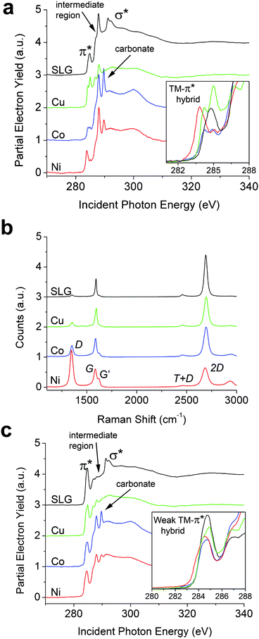 | ||
| Fig. 2 NEXAFS (85° incidence of the X-ray beam) and Raman spectra of SLG on Cu and transferred SLG on 300 nm SiO2/Si with 1 nm transition metal depositions labeled as such. (a) Spectrum SLG is a reference spectrum of graphene on 300 nm SiO2/Si with no metal deposition. (b) Raman shift of identical NEXAFS samples. Significant hybridization is seen as the appearance of shoulders on the G band and shifts in the 2D band. (c) Spectra correspond to 1 nm metal depositions of Ni, Co, and Cu on SLG/Cu. Spectrum SLG is a reference spectrum of SLG on Cu with no metal deposition. Peaks originating from thermal release tape are denoted in Fig. 2a and c as the “intermediate region”. | ||
Fig. 1 also presents data for few-layered graphene samples grown on single crystalline substrates. The lineshapes of the spectral features highlighted in the inset to Fig. 1a show a broader range of π* states (wider FWHM of π* resonance). The rigidity and incommensurability of the single crystalline substrates can lead to increased rippling of graphene, thereby giving rise to a range of interlayer separations, manifested in NEXAFS spectra as broadening of the π* resonance (furthermore, graphene on the single crystalline substrates is not entirely single-layered and the first and second layers could give rise to slightly different π* resonances).
A more pronounced broadening and the appearance of a low-energy shoulder to the π* feature (at 283.5 eV, lower than for graphene/Cu) is noted in C K-edge NEXAFS spectra for graphene on single crystalline Ni substrates. Ni[111] (a = 2.371 Å), the Ni facet that exhibits the best commensurability (1 × 1 commensurability)4 with the graphene lattice (a = 2.469 Å), shows the most pronounced low-energy shoulder for the π* resonance (Fig. 1b, inset) suggestive of orbital hybridization of a large proportion of the graphene carbon atoms with the underlying Ni lattice as a result of optimal registry and interfacial bonding of graphene. The distinctive low-energy shoulder to the π* resonance suggests that charge redistribution predominantly involves electron depletion from graphene, which thus uncovers a section of the occupied density of states (ODOS). The shifts seen in Fig. 1 are further validated with Raman spectroscopy (Fig. S1†), as discussed in detail below.
Given the growth-condition-dependent variations noted above, a better model system for fundamental studies of the nature of graphene–metal chemical bonding can be created by first transferring SLG (verified as such by Raman spectroscopy) to a weakly-interacting substrate such as amorphous SiO2 (equilibrium graphene separation is ca. 2.93 Å, binding energy of 15 meV per C atom),21 followed by substrate-cooled electron-beam evaporation of ultra-thin transition-metal layers to create an SLG–metal interface. NEXAFS dichroic ratio values as high as −0.85 (−0.97 for as-grown SLG/Cu samples) are achieved with the transfer processes, suggesting good substrate alignment but some remnant rippling of graphene.9 Such a graphene–metal interface also more accurately resembles metal-contacts that are applied to graphene for device measurements.15,20 Another difference from the samples noted in the previous section is that upon metal deposition onto graphene, given the high in-plane elastic moduli of graphene,33 the metal lattice adapts itself to the underlying substrate and is thus subject to concomitant strain, which is different from the situation with graphene grown on a metal substrate, wherein the graphene lattice is constrained to maintain the best possible commensurability with the underlying bulk metal lattice. Here, we have specifically investigated 1 nm Cu, Ni, and Co deposition on SLG transferred onto 300 nm SiO2/Si as well as for as-grown SLG on Cu (see ESI† for details). Fig. S3 and S4† show transition-metal L-edge spectra that enable interrogation of the extent of metal deposition (through evaluation of the edge jumps), which are found to be comparable within errors associated with macroscopic sampling, whereas atomic force microscopy images of the samples show island formation for all three metals but especially for Cu, which has the largest lattice mismatch with graphene.34
Fig. 2a displays the carbon K-edge NEXAFS spectra of transferred graphene with 1 nm electron-beam-evaporated Co, Cu, and Ni layers. The inset in Fig. 2a highlights the unambiguously greater perturbations of the graphene π cloud that are substantially stronger than those induced by chemical hybridization for graphene grown on metal foil and single-crystal substrates (Fig. 1). The distinct differences in hybridization of the three metals is clear from the inset of Fig. 2a as compared to single-layered graphene. All three transition metals distinctively broaden and split the π* resonance with the effect of Ni being the most pronounced, followed by Co and then Cu. When compared to the spectrum for SLG on SiO2 with no metal deposition, p-type doping of graphene (shift of electron density across the interfacial region) is characterized by enabling lower energy transitions to newly unoccupied bands, which predominates for the Ni-overlaid sample. In contrast, the π* resonance for Cu is shifted to slightly higher energies, suggestive of a lesser extent of charge redistribution. The effects of metal deposition on the excitonic σ* features are even more pronounced; a distinctive broadening and diminution of these features is noted, indicating a potential loss (or wider distribution) of excitonic confinement and substantial charge delocalization (and spread of this band to multiple unconfined states) as a result of orbital hybridization at the metal–SLG interface. A sharp resonance observed consistently in all the transferred samples at 288.0 eV arises from thermal release tape residue that inevitably somewhat contaminates the sample surface during transfer.9Fig. 2a also evidences a new feature that appears at ∼289.7 eV between the π* and σ* resonances upon transition metal deposition, which is entirely absent for the SLG sample on SiO2. This feature is well separated from the π* feature and most pronounced for Co and then Ni and only marginally observed upon deposition of Cu. Based on the lineshape and peak position, we tentatively ascribe this peak to transitions from 1s states to the anti-bonding orbitals of incipient carbonate linkages.35 Notably, the carbonates are not adsorbed impurities but originate specifically from oxidized carbidic linkages, which have been noted in XPS studies for graphene grown on Ni and upon deposition of Ti contacts.25,36 The increased tendency for carbide formation for Ni and Co in contrast to Cu parallels the formation energies calculated for both bulk and surface carbides.36 Carbide formation (and subsequent oxidation to the carbonate) is especially likely at the edges of the graphene islands as a result of the reaction between under-coordinated C and transition metal atoms.20,21,32
Raman spectroscopy data in Fig. 2b provide further insight into the nature of the transition metal–graphene interfaces.38–41 The G bands of Ni/SLG and Co/SLG exhibit a pronounced alteration with the appearance of a distinctive shoulder, suggestive of strong symmetry breaking and redistribution of electron density upon interfacial hybridization;37,42 in contrast, the splitting of the G band for the Cu-overlaid sample is barely discernible. Island coverage of the TMs (Ni and Co) on graphene and/or inhomogeneous p-doping is likely the cause of the bimodal G band. Further evidence for strong interfacial hybridization and the creation of incipient carbide linkages comes from the appreciable increase in the intensity of the D band as a result of symmetry breaking of the sp2-hybridized ring system, which occurs most notably for Ni/SLG and is negligible in Cu/SLG. The trend observed here thus also parallels the strength of the disruptive metal–carbon bonding (as discussed in more detail below), the DFT calculations of the binding energies, and energies of formation of the respective carbides.32,37
To further examine the availability of the graphene π cloud to hybridize with the apposite metal d-orbitals, the same three transition metals are also evaporated onto graphene grown on Cu, which retains some extent of hybridization with the underlying substrate (Fig. 1).9 While incipient carbonate peaks at ∼289.7 eV are indeed noted upon Ni and Co deposition in Fig. 2c (albeit at diminished relative intensities to Fig. 2a and not at all for Cu deposition), most remarkably, these systems exhibit no pronounced hybridization-induced splitting or shifts of the π* resonance as compared to substrate-decoupled graphene on 300 nm SiO2/Si (inset to Fig. 2c). In this case, the π cloud in SLG appears to be pinned to the Cu foil substrate after growth at 1000 °C; consequently, the π electron density in graphene is no longer available for interfacial hybridization with metal d-states, rendering, in a sense, the graphene “electronically less accessible” for chemical bonding. The corresponding Raman spectra are shown in Fig. S5† and show a similar doping trend as on 300 nm SiO2/Si. Comparison of Fig. 2a and c thus clearly illustrate that chemical bonding of evaporated metal atoms to graphene depends strongly on whether graphene resides on a SiO2 or a Cu substrate.
The pinning phenomenon and reduced electronic accessibility/interfacial hybridization of the graphene π cloud on Cu(η6-SLG)TM suggests a remarkable anisotropy in chemical bond formation as a function of coupling to the underlying substrate. The nature of transition metal bonding to single wall carbon nanotubes (SWNT) at metal contacts has been examined and known to form [(η6-SWNT)TM(η6-SWNT)] as electrical interconnections to SWNTs.43 Here we present evidence that TM(η6-SLG) likely forms for transition metals, but formation of TM(η6-SLG)TM* is hindered by the hybridized facet of graphene. Examining the nature of chemical bonding in the canonical organometallic compound bis(η6-benzene)chromium(0) (chromocene) with a sandwich structure provides an instructive analogy. Coordination of benzene ligands to Cr in the 18-electron bis(benzene)chromium(0) complex evinces classical umpolung behavior, rendering the benzene rings substantially less susceptible to electrophilic attack.44,45 As a case in point, further coordination of Cr to the unhindered face of the benzene ring to form “double-decker” complexes is not readily achieved. In this manner, the induced interfacial Cu–SLG hybridization reduces the accessibility of the graphene π orbitals for further interfacial bonding and consequently no characteristic splitting of the π* feature is observed upon deposition of metal overlayers.
The pronounced splitting of the C K-edge π* feature observed in the NEXAFS spectra (Fig. 2a) provides the most definitive evidence for perturbations of the graphene π* cloud upon metal deposition, and is further corroborated by the loss of excitonic confinement for the σ* feature, which suggests substantial rehybridization at graphene–metal contacts. To more rigorously examine the origin of this splitting and to evaluate the extent of interfacial hybridization, we have compared ab initio DFT calculations with our experimental C K-edge NEXAFS data.
In Fig. 3 the band structures for the ground state unit cells of each SLG–TM interfaces are presented along with the optimized geometries (dz) for Cu[111] (3.25 Å), Co(0001) (2.8 Å), and Ni[111] (2.1 Å).46 The flat dispersionless region (around the M point above Ef) shaded in orange in each of the plots is the main contributor to the observed π* and σ* peaks in the NEXAFS experiment. The alteration of these bands upon hybridization with transition metal 3d levels is clearly discernible in Fig. 3. The π* band on Cu is almost entirely overlaid with the metal sp states between M and K′ but does show greater energy dispersion than in SLG, suggesting one possible origin of the experimentally observed broadening of the π* resonance. Not surprisingly, varying dz for SLG/Cu from 2.1 Å to 6.0 Å strongly influences the extent of perturbation to the SLG band structure. An increase in dz reduces graphene–Cu interactions and leads to better retention of the dispersionless characteristic of the graphene π* feature (Fig. S6†). Dissimilar to Cu, Co and Ni have many coupled states as a result of significant perturbation to the original band structure of graphene, seen as avoided crossings between the original π* and σ* graphene bands. Substantial variation between spin major and spin minor channels is noted for graphene on Co, suggesting the possibility of spin-filtered transport at low biases. Such a rudimentary band structure analysis of the ground states of the graphene–metal interfaces thus is consistent with the experimentally observed greater perturbation of π* and σ* features evidenced upon Ni or Co deposition.
![Graphene–metal hybridized band structures at optimized distances and geometries for Cu[111], Co[0001], and Ni[111] graphene–metal interfaces. Cu and Ni are face-centered cubic (fcc) and Co is hexagonal-close packed (hcp) in 1 × 1 unit cells with single-layered graphene (SLG). Note that Co and Ni have contributions from spin major and spin minor bands. The π* band and σ* bands are investigated between the M and K points (orange area of band structures) in proximity to the Fermi level (set to zero energy and marked in each case with a dashed green line). We have denoted the carbon atom residing on top of a transition metal atom as the α-carbon and the atom residing atop a hollow site of the transition metal lattice as the β-carbon.](/image/article/2013/SC/c2sc21018e/c2sc21018e-f3.gif) | ||
| Fig. 3 Graphene–metal hybridized band structures at optimized distances and geometries for Cu[111], Co[0001], and Ni[111] graphene–metal interfaces. Cu and Ni are face-centered cubic (fcc) and Co is hexagonal-close packed (hcp) in 1 × 1 unit cells with single-layered graphene (SLG). Note that Co and Ni have contributions from spin major and spin minor bands. The π* band and σ* bands are investigated between the M and K points (orange area of band structures) in proximity to the Fermi level (set to zero energy and marked in each case with a dashed green line). We have denoted the carbon atom residing on top of a transition metal atom as the α-carbon and the atom residing atop a hollow site of the transition metal lattice as the β-carbon. | ||
For a more rigorous description of the splitting of the π* resonance, Fig. 4 depicts ab initio excited-state-core hole (XCH) X-ray absorption spectra (XAS) for large supercells derived from the ground state unit cells in Fig. 3. Each supercell (24.69 Å) contains 600 atoms (200 C and 400 transition-metal atoms), within which one carbon pseudopotential is altered to represent the photoabsorbing atom (see ESI†).
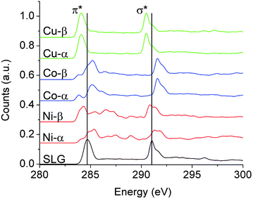 | ||
| Fig. 4 The calculated spectra corresponding to graphene–TM interfaces are depicted at 85° incidence for comparison with NEXAFS spectra in Fig. 3. Spectra have been separately calculated upon photoexcitation of α- or β-sublattice carbon atoms. The former reside atop a metal atom, whereas the latter resides on top of a hollow site. A 600 atom periodic supercell was used to model the spectra. The π* and σ* resonances change based on the specific transition metal and its equilibrium separation distance (dz) as well as the graphene sublattice. The rearrangement of electron density is highest for Ni, then Co, and is modest for Cu, which is consistent with our experimental results. The spectrum labeled SLG is simply a 200 carbon atom sheet where the transition metal atoms have been removed. Note each system exhibits the same spectral signature after the TM atoms are removed. | ||
The two symmetry equivalent atoms (denoted as α and β) in the graphene unit cell are distinctly hybridized to the transition metal lattice, breaking the symmetry of the graphene unit cell, and giving rise to distinctive spectral resonances for each sublattice, as well as for spin major and minor bands (Fig. 3 and 4). DFT calculations have validated the choice of geometry depicted in Fig. 3 (α-carbons directly above TM atoms and β-carbons in hollow sites), which is found to be energetically preferred over configurations placing both carbon atoms immediately above transition metal atoms or in a bridged position.4,20,21,23,24,28 The spectra in Fig. 4 suggest clear differences in the spectral signatures of the α- and β-carbon atoms, which are thus proposed to be another likely origin of the increased spectral structure observed upon metal deposition. The α- and β-carbons, especially for Ni and Co where dz is <2.8 Å, exhibit significant orbital hybridization with the d-states, a softening of the excitonic states, and shifts to relatively lower energy states; the shifts being a result of p-doping or electron depletion from graphene across the interfacial region. Interestingly, the β-carbon in Ni and Co is slightly screened from this interaction, retaining a higher energy and better defined π* resonance. Unlike Ni and Co, Cu exhibits a rigid band shift to lower energies with no new discernible resonances most likely because the optimal dz is large at 3.25 Å, suggesting only modest charge transfer, as further corroborated by the ground state band structures (Fig. 3 and 4). This rigid shift in both the π* and σ* features of graphene on Cu indicates an asymmetry in the electrostatics above and below the graphene plane, which must be screened within the plane itself such that the C 1s core-electron energy is less perturbed. This can be rationalized based on the limited spatial extent of the C 1s which is perhaps subject to less electrostatic perturbation by charge transfer from the TM, due to strong in–plane screening, in contrast to the more delocalized π* and σ* states. Indeed, the measured graphene/Cu spectra show features that lie significantly lower in energy than the expected π* feature of SLG, and the variability may easily arise from the distance dependence of this effect as indicated in Fig. S6.†
The atomic force microscopy (AFM) images in Fig. S3† suggest island formation upon metal deposition, which could possibly leave discrete regions of the underlying graphene uncovered. Distinctive signals from hybridized and non-bonded regions can give rise to characteristic signatures in the π* region of the C K-edge spectra. The increased complexity of the π*spectral signatures is likely a result of a combination of the SLG spectrum with the corresponding spectra for the α and β graphene sublattices hybridized with TMs. An analogous argument can be made for graphene grown (and sitting atop) on Cu and Ni foils or single crystals wherein a certain fraction of the atoms are in close registry with the metal surface, and thus exhibit a strong wave-function overlap, whereas other regions of graphene are buckled and reside at various equilibrium separations from the substrate.4 Upon calculated alignment with reference to an isolated carbon atom,47 the modeled spectra in Fig. 4 show substantial shifts in peak positions for the metal-hybridized carbon atoms as compared to free-standing graphene.
The progressive diminution of π* splitting from Ni and Co to Cu further correlates well with the expected strength of interfacial dipoles predicted by DFT calculations. Khomyakov et al. and Giovanetti et al. recently analyzed the strengths of interfacial dipoles and charge redistribution at graphene–metal interfaces for a series of TMs, which parallels the trend observed in our experimental data; Ni, Co, and Cu create interfacial dipoles of ±0.021 e (p-type), ±0.022 e (p-type), and ±0.008 electrons (e) per carbon atom (n-type), respectively.20,21 Graphene interfaced with Cu can be n-type doped (dz < 3.4 Å) or p-type doped (dz > 3.4 Å) depending upon the equilibrium separation.21 Experimentally, we observe comparable interfacial bonding for Ni and Co (modestly higher for Ni), which eclipses the splitting of the π* resonance evinced for Cu upon deposition onto graphene (Fig. 2a). The pronounced shift of the π* resonance to lower energies upon extensive p-type doping, such as achieved with deposition of Ni and Co overlayers, is induced by unveiling of a portion of the filled (valence band) Dirac cone.10 As graphene loses electron density to the metal overlayers, sections of the depleted valence band become accessible to a 1s core electron excited in a NEXAFS experiment, and thus new pre-edge absorbance to the fundamental π* resonance are observed. The calculated XCH spectra in conjunction with the experimental results suggests that the observed splitting and increased spectral structure of the π* NEXAFS resonance of graphene–metal interfaces can be attributed to a combination of (a) variations in the equilibrium separation (dz) of graphene and the metal (or different extents of metal coverage on graphene), (b) distinctive signals from inequivalent carbon atoms on the α and β lattices as a result of the breaking of symmetry and loss of degeneracy; and (c) distinctive hybridization of spin-major and spin-minor bands for the Co and Ni cases.
Conclusions
Interfacing a transition metal as a contact to graphene is central to fundamental science for interrogating the transport properties of graphene and is also imperative for technological applications of this material in microelectronics and spintronics. The comprehensive NEXAFS analysis of graphene–metal interfaces presented here provides detailed experimental evidence of perturbations introduced to the graphene electronic structure upon metal deposition. Graphene–metal bonding has been examined for graphene grown on single crystalline metal substrates, graphene grown on polycrystalline foils, and graphene with overdeposited metal adatoms. Strong covalent hybridization is noted upon deposition of metal atoms onto graphene on SiO2, far exceeding graphene–metal bonding evidenced at single crystal and polycrystalline foil substrates. Specifically, a sharp splitting of the π* resonance implies substantial wavefunction overlap between the graphene π cloud and transition metal d orbitals as a result of hybridization-induced symmetry breaking of the two-atom graphene unit cell and charge redistribution across the interfacial region. Raman spectroscopy results corroborate perturbation of the graphene π cloud and initiation of metal–carbon bond formation (including formation of incipient carbidic linkages) for Ni/SLG and Co/SLG contacts. Taken together, the picture that emerges suggests that Cu–graphene interfaces primarily evidence modest charge redistribution and a limited extent of orbital hybridization, which is mostly consistent with the physisorption picture but indicates a finite role for wavefunction overlap rather than simply a rigid band shift model. In contrast, at Ni/SLG and Co/SLG contacts, the π cloud is substantially distorted due to hybridization with the transition metal d-states and a clear loss of excitonic confinement is evidenced for the σ* states. Spin-majority and spin-minority bands of Ni and Co are further deduced to couple distinctively to graphene. For single-crystalline substrates, the strongest hybridization of graphene is observed to Ni[111], which presents the most commensurate crystallographic facet to the graphene lattice. Our results also demonstrate that substrate coupling of graphene to an underlying layer can substantially reduce the electronic accessibility of the exposed layer for further chemical bonding. This pinning of the graphene π-electron density suggests opportunities for anisotropic functionalization or protection of individual faces of graphene and suggests that an underlying metal substrate can act as the equivalent of a “protecting group”.Experimental
Graphene was grown on Cu and Ni substrates under ambient pressure in a hot-wall tube furnace by a thermal decomposition process using a mixture of precursor gases, Ar–H2–CH4, as described previously in the literature.48,49 Transfer of graphene to 300 nm SiO2/Si substrate was performed only for SLG grown on Cu substrates. Transfer was achieved by applying thermal release tape (TRT, item NO.319Y – 4MS, Nitto Denko Corp.) to SLG/Cu and subsequently etching the Cu foil with ∼0.5 M FeCl3 solution for a few hours.48 The SLG/TRT was subsequently washed in a 5% HCl solution and with copious amounts of deionized water, and then dried and roll-pressed onto a 300 nm SiO2/Si substrate. The samples were then heated in a conventional oven to the TRT release temperature. After release of the graphene, the samples were heated in the tube furnace under vacuum at 225 °C for 1 h. Subsequently, the samples were coated with 1 nm of Co, Cu, or Ni using electron-beam evaporation under ultra-high vacuum (<10−6 Torr) conditions. The substrates were cooled using flowing water during the deposition process.We calculate DFT ground-state energies, and optimized geometries using plane-wave basis sets in the Quantum Espresso suite of codes within the pseudopotential approximation.49 All calculations were performed within the generalized-gradient approximation to the exchange-correlation potential according to Perdew, Burke, and Ernzerhof (PBE).51 Spin-polarized calculations were performed for graphene on Co and Ni. The ground-state band structures are formulated from 4 atomic layers of each transition metal with a layer of carbon atoms on top where the vacuum region is ∼10 Å. The interfacial distances of 2.1 Å (Ni), 2.8 Å (Co), and 3.25 Å (Cu) were taken from Olsen et al., where the random phase approximation (RPA) was used to account for both chemical bonding and van der Waals interactions at the interface.46 To model metal deposited onto graphene, the graphene unit cell (2.469 Å) is held constant and the geometry of the metal overlayers and interface is energetically optimized.
The Fermi's Golden rule expression for X-ray absorption cross-section was modeled from first-principles using the excited electron and core-hole (XCH) approach to model electronic transitions from 1s to 2p character projected on individual carbon atoms, previously reported by some of the authors.10,29 The final state of the electronic system is calculated in the presence of a core-hole (derived from an altered carbon pseudopotential with 1s12s22p2 configuration) surrounded by a multitude of ground state atoms within a large periodic supercell (24.69 Å, 600 atoms). Self-consistent DFT relaxes the electronic structure around the excited carbon atom, with explicit inclusion of the excited electron.50 The energies of α- and β-carbons and the energies of SLG/Co, SLG/Cu, and SLG/Ni are chemically shifted according to a previously established method by some of the authors of this work.47 After this computed chemical alignment, a global shift is performed to align the π* peak in SLG with experiment for SLG on 300 nm SiO2/Si.
Acknowledgements
We acknowledge the New York State Energy Research and Development Authority for partial support of this work. Certain commercial names are presented in this manuscript for purposes of illustration and do not constitute an endorsement by NIST. Density functional theory simulations were performed as a User Project at the Molecular Foundry, Lawrence Berkeley National Laboratory, which is supported by the Office of Science, Office of Basic Energy Sciences, of the U.S. Department of Energy, under Contract No. DE-AC02-05CH11231.Notes and references
- A. K. Geim and K. S. Novoselov, Nat. Mater., 2007, 6, 183–191 CrossRef CAS.
- A. K. Geim, Science, 2009, 324, 1530–1534 CrossRef CAS.
- J.-H. Chen, C. Jang, S. Adam, M. S. Fuhrer, E. D. Williams and M. Ishigami, Nat. Phys., 2008, 4, 377–381 CrossRef CAS.
- J. Wintterlin and M.-L. Bocquet, Surf. Sci., 2009, 603, 1841–1852 CrossRef CAS.
- S. Garaj, W. Hubbard, A. Reina, J. Kong, D. Branton and J. A. Golovchenko, Nature, 2010, 467, 190–193 CrossRef CAS.
- E. J. H. Lee, K. Balasubramanian, R. T. Weitz, M. Burghard and K. Kern, Nat. Nanotechnol., 2008, 3, 486–490 CrossRef CAS.
- A. Castro Neto, F. Guinea, N. Peres, K. Novoselov and A. Geim, Rev. Mod. Phys., 2009, 81, 109–162 CrossRef CAS.
- P. Avouris, Nano Lett., 2010, 10, 4285–4294 CrossRef CAS.
- V. Lee, C. Park, C. Jaye, D. A. Fischer, Q. Yu, W. Wu, Z. Liu, J. Bao, S.-S. Pei, C. Smith, P. Lysaght and S. Banerjee, J. Phys. Chem. Lett., 2010, 1, 1247–1253 CrossRef CAS.
- B. J. Schultz, C. J. Patridge, V. Lee, C. Jaye, P. S. Lysaght, C. Smith, J. Barnett, D. A. Fischer, D. Prendergast and S. Banerjee, Nat. Commun., 2011, 2, 372 CrossRef.
- H. B. Heersche, P. Jarillo-Herrero, J. B. Oostinga, L. M. K. Vandersypen and A. F. Morpurgo, Nature, 2007, 446, 56–59 CrossRef CAS.
- J. Xue, J. Sanchez-yamagishi, D. Bulmash, P. Jacquod, A. Deshpande, K. Watanabe, T. Taniguchi, P. Jarillo-herrero and B. J. Leroy, Nat. Mater., 2011, 10, 282–285 CrossRef CAS.
- A. Varykhalov, J. Sánchez-Barriga, A. Shikin, C. Biswas, E. Vescovo, A. Rybkin, D. Marchenko and O. Rader, Phys. Rev. Lett., 2008, 101, 1–4 Search PubMed.
- B. Uchoa, V. Kotov, N. Peres and A. Castro Neto, Phys. Rev. Lett., 2008, 101, 026805 CrossRef.
- S. Barraza-Lopez, M. Vanević, M. Kindermann and M. Y. Chou, Phys. Rev. Lett., 2010, 104, 076807 CrossRef.
- Y. Dedkov, M. Fonin, U. Rüdiger and C. Laubschat, Phys. Rev. Lett., 2008, 100, 107602 CrossRef.
- N. Tombros, C. Jozsa, M. Popinciuc, H. T. Jonkman and B. J. van Wees, Nature, 2007, 448, 571–574 CrossRef CAS.
- A. Krasheninnikov, P. Lehtinen, A. Foster, P. Pyykkö and R. Nieminen, Phys. Rev. Lett., 2009, 102, 126807 CrossRef CAS.
- K. Pi, K. McCreary, W. Bao, W. Han, Y. Chiang, Y. Li, S.-W. Tsai, C. Lau and R. Kawakami, Phys. Rev. B: Condens. Matter Mater. Phys., 2009, 80, 625–630 CrossRef.
- G. Giovannetti, P. Khomyakov, G. Brocks, V. Karpan, J. van den Brink and P. Kelly, Phys. Rev. Lett., 2008, 101, 4–7 Search PubMed.
- P. Khomyakov, G. Giovannetti, P. Rusu, G. Brocks, J. van den Brink and P. Kelly, Phys. Rev. B: Condens. Matter Mater. Phys., 2009, 79, 195425 CrossRef.
- Q. J. Wang and J. G. Che, Phys. Rev. Lett., 2009, 103, 066802 CrossRef CAS.
- D. Eom, D. Prezzi, K. T. Rim, H. Zhou, M. Lefenfeld, S. Xiao, C. Nuckolls, M. S. Hybertsen, T. F. Heinz and G. W. Flynn, Nano Lett., 2009, 9, 2844–2848 CrossRef CAS.
- C. Gong, G. Lee, B. Shan, E. M. Vogel, R. M. Wallace and K. Cho, J. Appl. Phys., 2010, 108, 123711 CrossRef.
- A. Preobrajenski, M. L. Ng, A. S. Vinogradov and N. Mårtensson, Phys. Rev. B: Condens. Matter Mater. Phys., 2008, 78, 073401 CrossRef.
- A. Grüneis and D. Vyalikh, Phys. Rev. B: Condens. Matter Mater. Phys., 2008, 77, 193401 CrossRef.
- D. Pacilé, M. Papagno, A. Rodríguez, M. Grioni, L. Papagno, Ç. Girit, J. Meyer, G. Begtrup and A. Zettl, Phys. Rev. Lett., 2008, 101, 066806 CrossRef.
- G. Bertoni, L. Calmels, A. Altibelli and V. Serin, Phys. Rev. B: Condens. Matter Mater. Phys., 2005, 71, 075402 CrossRef.
- D. Prendergast and G. Galli, Phys. Rev. Lett., 2006, 96, 215502 CrossRef.
- J. Chen, Surf. Sci. Rep., 1997, 30, 1–152 CrossRef CAS.
- J. Stohr, NEXAFS Spectroscopy, Springer, Berlin, 1992 Search PubMed.
- H. Valencia, A. Gil and G. Frapper, J. Phys. Chem. C, 2010, 114, 14141–14153 CAS.
- C. Lee, X. Wei, J. W. Kysar and J. Hone, Science, 2008, 321, 385–388 CrossRef CAS.
- R. Zan, U. Bangert, Q. M. Ramasse and K. S. Novoselov, J. Phys. Chem. Lett., 2012, 3, 953–958 CrossRef CAS.
- J. A. Brandes, S. Wirick and C. Jacobsen, J. Synchrotron Radiat., 2010, 17, 676–682 CrossRef CAS.
- A. Pirkle, R. M. Wallace and L. Colombo, Appl. Phys. Lett., 2009, 95, 133106 CrossRef.
- G. R. Darling, R. W. Joyner and J. B. Pendry, Stud. Surf. Sci. Catal., 1989, 48, 335–345 CrossRef.
- L. S. Panchakarla, K. S. Subrahmanyam, S. K. Saha, A. Govindaraj, H. R. Krishnamurthy, U. V. Waghmare and C. N. R. Rao, Adv. Mater., 2009, 560012, 4726–4730 Search PubMed.
- A. Das, S. Pisana, B. Chakraborty, S. Piscanec, S. K. Saha, U. V. Waghmare, K. S. Novoselov, H. R. Krishnamurthy, A. K. Geim, A. C. Ferrari and A. K. Sood, Nat. Nanotechnol., 2008, 3, 210–215 CrossRef CAS.
- K. K. Kim, A. Reina, Y. Shi, H. Park, L.-J. Li, Y. H. Lee and J. Kong, Nanotechnology, 2010, 21, 285205 CrossRef.
- A. Ferrari, Solid State Commun., 2007, 143, 47–57 CrossRef CAS.
- S. Bae, H. Kim, Y. Lee, X. Xu, J.-S. Park, Y. Zheng, J. Balakrishnan, T. Lei, H. Ri Kim, Y. I. Song, Y.-J. Kim, K. S. Kim, B. Özyilmaz, J.-H. Ahn, B. H. Hong and S. Iijima, Nat. Nanotechnol., 2010, 5, 574–578 CrossRef CAS.
- F. Wang, M. E. Itkis, E. B. Bekyarova, X. Tian, S. Sarkar, A. Pekker, I. Kalinina, M. L. Moser and R. C. Haddon, Appl. Phys. Lett., 2012, 100, 223111 CrossRef.
- D. Seyferth, Organometallics, 2002, 21, 2800–2820 CrossRef CAS.
- S. Sarkar, S. Niyogi, E. Bekyarova and R. C. Haddon, Chem. Sci., 2011, 2, 1326 RSC.
- T. Olsen, J. Yan, J. Mortensen and K. Thygesen, Phys. Rev. Lett., 2011, 107, 1–5 CrossRef.
- A. H. England, A. M. Duffin, C. P. Schwartz, J. S. Uejio, D. Prendergast and R. Saykally, Chem. Phys. Lett., 2011, 514, 187–195 CrossRef CAS.
- Y. Lee, S. Bae, H. Jang, S. Jang, S.-E. Zhu, S. H. Sim, Y. I. Song, B. H. Hong and J.-H. Ahn, Nano Lett., 2010, 10, 490–493 CrossRef CAS.
- S. Bhaviripudi, X. Jia, M. S. Dresselhaus and J. Kong, Nano Lett., 2010, 10, 4128–4233 CrossRef CAS.
- P. Giannozzi, S. Baroni, N. Bonini, M. Calandra, R. Car, C. Cavazzoni, D. Ceresoli, G. L. Chiarotti, M. Cococcioni, I. Dabo, A. Dal Corso, S. de Gironcoli, S. Fabris, G. Fratesi, R. Gebauer, U. Gerstmann, C. Gougoussis, A. Kokalj, M. Lazzeri, L. Martin-Samos, N. Marzari, F. Mauri, R. Mazzarello, S. Paolini, A. Pasquarello, L. Paulatto, C. Sbraccia, S. Scandolo, G. Sclauzero, A. P. Seitsonen, A. Smogunov, P. Umari and R. M. Wentzcovitch, J. Phys.: Condens. Matter, 2009, 21, 395502 CrossRef.
- J. Perdew, K. Burke and M. Ernzerhof, Phys. Rev. Lett., 1996, 77, 3865–3868 CrossRef CAS.
Footnote |
| † Electronic supplementary information (ESI) available. See DOI: 10.1039/c2sc21018e |
| This journal is © The Royal Society of Chemistry 2013 |