Cu2ZnSnS4 thin films: spin coating synthesis and photoelectrochemistry†
Jing Wang,
Peng Zhang*,
Xuefeng Song and
Lian Gao*
State Key Lab of Metal Matrix Composites, School of Materials Science and Engineering, Shanghai Jiao Tong University, 800 Dongchuan Rd., Shanghai, P. R. China 200240. E-mail: liangao@mail.sic.ac.cn; pengzhang2010@sjtu.edu.cn
First published on 30th April 2014
Abstract
Cu2ZnSnS4 (CZTS) has attracted great interest in both photovoltaic and photoelectrochemical applications as a low cost and environmentally-friendly solar absorber material. The development of a facile and green chemical route for the preparation of a well crystallized and stable CZTS photoelectrode still remains a challenge. We present here the preparation of well crystallized CZTS thin films using a facile spin-coating method based on methanol solution and their applications as photoelectrocathodes for hydrogen production. The bare CZTS thin films demonstrate outstanding photoelectrochemical (PEC) efficiency and chemical stability, which are further improved by surface modification of CdS and TiO2 layers using chemical bath and atomic layer deposition, respectively. The incident-photon-to-current efficiency (IPCE) and long term photoelectrochemistry of the CZTS thin films are measured. The characterization of XRD, Raman, SEM, and UV-vis absorption is also performed.
Introduction
The direct conversion of solar to chemical energy through a photoelectrochemical (PEC) process has long been a target of researchers, which represents a green and renewable path to produce hydrogen and/or oxygen. Since the pioneering work of hydrogen production on TiO2,1 many oxide semiconductors have been investigated as photoelectrodes, e.g. TiO2,2 WO3,3 Cu2O,4 Fe2O3,5,6 BiVO4.7 However, none of the semiconductor has been proved to be ideal photoelectrocatalyst due to the limitations in either band gap, chemical stability, electron conductivity, or safety. Chalcogenide semiconductors represent one of great candidates for applications in PEC reaction due to their proper band potentials and absorption properties in the visible region. The relatively negative potential of S3p makes sulfides good photocatalysts for solar water splitting. CdS, e.g. has been proved to be an almost ideal photoelectrocatalyst for solar hydrogen production.8,9 However, the photocorrosion of S2− and the toxicity of Cd element remain an obstacle for their commercial applications. Exploration of other sulfides with environmental friendly elements and chemical stability, therefore, arouses great attentions.Cu(InGa)Se2 (CIGS) has been applied in sustainable high-efficiency solar cells and used as a PEC photocathode.10,11 Owing to the scarcity and high cost of In and Ga elements in CIGS, another compound with similar structure, Cu2ZnSnS4 (CZTS), has attracted intense emphasis as visible light absorber material with earth-abundant and environment-friendly compositions. CZTS possesses a high absorption coefficient of over 104 cm−1 and optimal band gap of approximately 1.5 eV.12–14 This p-type semiconductor was originally applied as solar absorber in solar cells. Great progress in the efficiencies has been achieved. Katagiri et al.15 prepared CZTS solar cells by sputtering and vapor deposition with an efficiency of 6.7%. Recently, an efficiency of 12.0% have been achieved in Cu2ZnSn(Se,S)4 solar cells after optical-designing.16
The direct applications of CZTS in photoelectrochemical reaction have been recently investigated and the preparation methods been extended to ambient conditions. In 2008, Scragg et al.17 investigated PEC Eu3+ reduction of CZTS prepared by electroplating metallic precursors sequentially following by sulfurization. Yokoyama et al.18 reported H2 evolution for the first time on co-sputtered CZTS thin films with the structure of Pt/TiO2/CdS/CZTS/Mo, and a solar-to-H2 conversion efficiency of 1.2% was obtained.
CZTS thin films were generally prepared by directly depositing the compound on substrates through physical or chemical deposition under vacuum. Various non-vacuum methods have now been developed to lower the cost of preparation. Electrodeposition,19 successive ionic layer adsorption reaction (SILAR),20 sol–gel spin coating,21 and true solution22 etc. have been reported. In many cases, toxic H2S stream is needed to sulfidize the compounds. During PEC application, large dark currents were often observed due to the photocorrosion of the sulfides and/or the presence of pinholes. The chemical stability of this compound as PEC material therefore still remains a challenge. Porous nanocrystalline Cu2ZnSnS4 films, prepared by a facile metal organic decomposition (MOD) method,23 have showed superior performance to a dense one. However, a continuous degradation on the photocurrent is still observed.
Herein, we adopted a facile spin coating method to directly synthesize CZTS thin films without further H2S treatment. The thin films show very small dark current and outstanding efficiencies during PEC reaction in basic electrolyte. The surface modification with CdS and TiO2 on CZTS electrodes have been shown to improve both the efficiencies and the stabilities of this sulfide photoelectrode.
Experimental section
Synthesis of CZTS film
Copper(II) dichloride dihydrate (CuCl2·H2O), zinc chloride (ZnCl2), tin(II) chloride dihydrate (SnCl2·H2O) and thiourea (CH4N2S) were purchased from Sinopharm Chemical Reagent Co., Ltd and used without further purification. They were used as precursors for CZTS. Thiourea (1 mol L−1), zinc chloride (0.2 mol L−1), tin dichloride (0.15 mol L−1) and copper dichloride (0.15 mol L−1) were dissolved in absolute methanol (50 mL) as precursor solution. The fluorine-doped SnO2 (FTO) substrates were cleaned successively with acetone, ethanol, and Milli-Q water by ultra-sonication and dried with nitrogen blow. Subsequently, the precursor solution was spin coated on FTO at 2000 rpm for 20 s, then heated at 150 °C in air. The spin coating and drying can be repeated several times to obtain desired thicknesses. The as-synthesized CZTS thin films were then annealed at 350 °C in argon for 1 h at a heating rate of 5 °C min−1. After cooling to room temperature, the color of CZTS thin film turned from dark yellow to shiny black.Chemical bath deposition (CBD) for CdS
CdS coating layer was prepared by chemical bath deposition. The as-prepared CZTS film on FTO glass was submerged into the CBD solution containing CdI2, NH4I, Thiourea, and ammonia. After deposition, the substrate was taken out, rinsed with Milli-Q water and dried with nitrogen blow. The CZTS/CdS thin film was then heated at 200 °C for 30 min in air.Atomic layer deposition (ALD) of TiO2
TiO2 protective layer deposited on CZTS/CdS thin films using an ALD system (Savannah 100, Ultratech, USA). Titanium dioxide (TiO2) was deposited at 200 °C, using tetrakis-dimethylamino titanium (TDMAT) and H2O as Ti and O precursors, respectively. Exposed substrate was masked with Kapton tape prior to deposition. TiO2 was deposited in pulse mode under a nitrogen flow of 20 sccm. TDMAT was held in the chamber for 0.1 s, then H2O was persisted for 0.015 s, and the wait period of 10 seconds for both precursors. The growth rate per cycle (GPC) for TiO2 was 0.4 Å per cycle at 200 °C. The TiO2 deposition was performed for 500 circles and a layer thickness of 20 nm is achieved.Characterization of the thin films
The crystallographic structures of the as-synthesized thin films were identified by X-ray diffraction (XRD, Ultima IV, Rigaku Co., Ltd., Japan Cu Kα, λ = 1.54178 Å). The phase was confirmed by Raman spectrometer (Bruker Optics Senterra R200-L). Scanning electron microscope (SEM) images and energy-dispersive X-ray spectroscopy (EDS) of the as-obtained products were performed on NOVA Nano SEM 230 and X-Max80, respectively. UV-vis absorption was carried out by UV-vis spectroscopy (UV-2450).Photoelectrochemical (PEC) measurements
All PEC measurements were performed using a three-electrode experimental setup (CHI660D electrochemical workstation, Chenhua, Shanghai) using a side window of a xenon lamp (300 W, Newport 6258, USA) as light source. A platinum wire and a saturated calomel electrode (SCE) acted as the counter and reference electrode, respectively. The Eu(NO3)3·6H2O aqueous solution (0.1 mol L−1) and Na2SO4 (0.2 mol L−1) were both used as electrolytes.Results and discussion
X-ray diffraction (XRD) pattern of the as-synthesized CZTS thin film on glass is shown in Fig. 1. Since the FTO substrate has strong diffraction which blurs the diffraction pattern of the CZTS deposited on it, we show the XRD on the CZTS/glass instead. The diffraction peaks of the thin film sample agree well with the kesterite CZTS (JCPDS, Card, no. 26-0575). The broadened diffraction indicates a nanocrystalline nature of the obtained thin films. The average size of the nanocrystal estimated using Scherrer's equation and Williamson–Hall method is ∼4.9 and 5.5 nm, respectively. Since the X-ray diffraction peaks are close to those of ZnS (JCPDS, Card, no. 65-0309) and Cu2SnS3 (JCPDS, Card, no. 27-0198). Raman spectrum is characterized to verify the presence of CZTS structure, as shown in Fig. 2. The scattering at 329 cm−1 is identical to the literature values of CZTS.24 The 9 cm−1 red shift relative to the reported bulk may be due to the size effect.25 The absence of peaks at 278 cm−1, 351 cm−1 and 295–303 cm−1, 355 cm−1 suggests the absence of ZnS and Cu2SnS3 in the sample.25 The XRD and Raman results indicate that the main phase of sample is CZTS.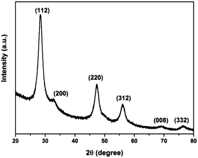 | ||
| Fig. 1 XRD pattern of as-synthesized CZTS thin film on glass. | ||
 | ||
| Fig. 2 Raman spectrum of CZTS thin film on glass. | ||
The surface SEM images of CZTS thin films are shown in Fig. 3. The samples display a compact feature without any trace of cracks or nanostructures. The cross-sectional image of the thin film, Fig S1 in ESI,† also shown relatively smooth surface and a compact planar morphology of the thin film with no porosity. The average crystal size of 5 nm estimated from XRD patterns therefore indicates a compact polycrystalline nature of the thin films. Holes with diameters of 150–250 nm are observed on the smooth surface of the thin films. These holes might be formed due to the evaporation of the solvents when the thin films were annealed in argon. This is an interesting result because generally porous structures or cracks were resulted upon decomposition of extra sulfur precursors (TAA or thiourea) and solvents.23,26,27 A higher surface area in porous structures was proposed to lead to an enhanced photoelectrochemical solar energy conversion efficiency due to a higher density of surface reaction centres.23 However, an obvious attenuation on the photocurrent is also observed in continuous illumination of the porous CZTS photocathode. The smooth surface observed in SEM images is consistent with the shiny feature of the thin films shown in Fig. S1.†
 | ||
Fig. 3 The surface SEM images of the CZTS thin film. (a) 5000×; (b) 25![[thin space (1/6-em)]](https://www.rsc.org/images/entities/char_2009.gif) 000×; (c) 50000×; (d) 100000×. Compact and smooth surface is observed with some well dispersed holes ranging from 100–150 nm in diameter. 000×; (c) 50000×; (d) 100000×. Compact and smooth surface is observed with some well dispersed holes ranging from 100–150 nm in diameter. | ||
The optical band gaps of CZTS thin films can be evaluated by its UV-vis absorption spectra, Fig. 4. The band gap (Eg) of a semiconductor can be estimated by eqn (1)17
| (αhυ)2 = A(hυ − Eg) | (1) |
 | ||
| Fig. 4 UV-vis absorption spectra of the as-synthesized CZTS thin film(s) at room temperature. Insert shows the plot of (αhυ)2 vs. photon energy. | ||
As a p-type chalcogenide semiconductor, CZTS thin films have the common disadvantage in chemical stability during PEC reaction due to the probable photocorrosion of S2− and Cu+, and fast attenuation is often observed in bare CZTS photoelectrodes.29 For improvement of photocurrent, a layer of CdS is generally coated on the surface of the CZTS to build an inner p–n junction, which facilitates the separation of the photon-generated electrons and holes by the built-in electric field. A top layer of TiO2 is also applied to further direct the transfer of photoelectrons to the electrolyte and to separate the sulfides from the electrolyte. The CdS and TiO2 layer thus not only help the separation and transfer of photogenerated charges from the bulk onto solid–liquid interfaces, but protect the CZTS thin films from reaction with the electrolytes.
The photoelectrochemical performance of these compact planar photocathodes for water splitting were characterized by measurement of photocurrents as a function of applied bias, as shown in Fig. 5. The negative photocurrents detected in all the three samples indicate cathodic surface reactions, that is, proton reduction on the working electrodes. The chopped I–V curves of CZTS, CZTS/CdS, and CZTS/CdS/TiO2 all show very small dark currents, which indicates a neglectable corrosion during the I–V characterization. Comparing with the unprotected CZTS photocathodes in other reports,18,29,30 the as prepared CZTS thin films show superior resistance to photocorrosion. This is ascribable to the compact and crackless feature of the thin films, Fig. 3, therefore play no bad on the PEC performance, and should not be pinholes as observed in many reports. The compact thin films prepared in this facile spin coating method therefore demonstrate an outstanding chemical stability in PEC reactions. Under illumination of 15 mW cm−2 and an applied bias of 0 VRHE, the photocurrents of CZTS, CZTS/CdS, and CZTS/CdS/TiO2 are 0.125, 0.138, and 0.165 mA cm−2, respectively. The coating of CdS and TiO2 layer improves the conversion efficiencies of the CZTS thin films. The enhancement on the photocurrent by additional surface layers is more notable at lower bias. The cathodic photocurrents at 0.2 VRHE are increased by ca. 2.7 and 3.3 times after deposition of CdS and TiO2 sequentially. The improvement of the photocurrent upon deposition of CdS is due to the built-in p–n junctions between CZTS and CdS, which help separation of the generated electron–hole pairs in the depletion zone. At higher bias, e.g.-0.05 VRHE, the photocurrent of CZTS is very close to CZTS/CdS. This indicates the saturation of the photocurrents. Coating of TiO2 layer further enhances the photocurrents at the whole range of applied bias and shifts the onset potential of the photocurrents from 0.48 VRHE to 0.68 VRHE. The onset potential of 0.68 VRHE can be a coarse approximation of the flat band potential and valance band potential. Considering the band gap of CZTS of ∼1.5 V, the conduction band potential is ∼−0.8 VRHE, which is negative enough for hydrogen production in a large range of pH values. This is consistent with the report by Scragg17 and Rovelli.29 The shift of the onset potential as well as the significant improvement on the photocurrents at low applied bias could both be attributed to fluent transfer of electrons through the conduction band of TiO2 to the electrolyte.18 The charge accumulation on interfaces thus diminished, which can be confirmed from the apparent disappearing of the transient photocurrents on CZTS/CdS/TiO2. The photocurrent transients, observed in the first moment of light on or off during chopped illumination, are closely related to the level of surface defects.5 Therefore, coating of TiO2 layer significantly diminishes the surface defects and facilitates the transfer of electrons.
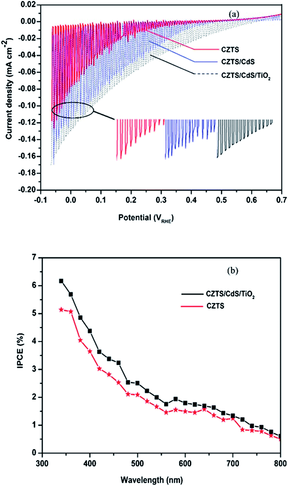 | ||
| Fig. 5 (a) Chopped photocurrents of CZTS, CZTS/CdS, CZTS/CdS/TiO2 thin films as a function of applied bias (vs. VRHE) in a conventional three electrode configuration. The potential was swept at 0.01 V s−1 toward positive potential. Light intensity, 15 mW cm−2; electrolyte, 0.2 mol L−1 Na2SO4 aqueous solution. (b) IPCE of CZTS and CZTS/CdS/TiO2 samples at 0 VRHE in 0.2 mol L−1 Na2SO4 aqueous solution. | ||
The incident-photon-to-current efficiencies (IPCE) for both bare CZTS and CZTS/CdS/TiO2 are shown in Fig. 5(b). The IPCE of CZTS/CdS/TiO2 is 5.0% at 380 nm, 0 VRHE, which is 1.2 times that of bare CZTS. This IPCE is still smaller than reported planar CZTS prepared using physical sputtering techniques with CdS and TiO2 coating.18 This could be due to the polycrystalline nature of the thin films that we prepared using wet chemical method. The polycrystalline thin films might possess relatively higher density of high-angle grain boundaries than the physically deposited thin films followed by high temperature sulfurization. The high-angle grain boundaries was proposed to possess the high energy barriers that hinder the charge transport among crystals.31 The CZTS thin films prepared using electrochemical deposition on Mo substrate with CdS and TiO2 layer showed an IPCE of ∼10% at 380 nm, −0.4 V Ag/AgCl, in 0.1 M Eu3+ solution.29 This is comparable with the 5.0% for water splitting in our case considering the fast kinetics of the Eu3+ reduction. The obtained IPCE of this compact thin film is higher than the 4.2% of the mesoporous CZTS thin films measured at −0.4 VRHE on 380 nm in 0.5 M Na2SO4.23
Various photocurrents for the bare CZTS thin film prepared using different methods have been reported, as summarized in Table 1.18,23,29,30 The bare CZTS thin films presented herein is superior to most of the other works based on solution methods. We propose that a relative better crystallization of the thin films facilitates charge transport from bulk to the solid–liquid interfaces due to the lower density of defects and grain boundaries. The limited surface area is obviously a disadvantage in PEC reaction because the number of the surface active sites for hydrogen production is less than the porous structures. Therefore, the improvement of the photocurrent after deposition of CdS and TiO2 layer is limited comparing to the samples with higher surface areas, which could be 2 orders of magnitude.29 However, a higher surface area in porous CZTS photocathodes also indicates a higher opportunity in surface chemical corrosion, which thus causes problem in the long term chemical stability.
| Ref. | Photointensity | Methods of CZTS preparation | Photocathode structure | Photocurrents at 0 VRHE |
|---|---|---|---|---|
| 30 | 300 W xenon lamp | Sequential electrodeposition following sulfuration at 550 °C | Pt/CdS/CZTS/Mo-mesh | 1.92 mA cm−2 |
| 18 | AM 1.5 | Co-sputtering technique | Pt/CZTS | Very small |
| Pt/CdS/CZTS | 2 mA cm−2 | |||
| Pt/TiO2/CdS/CZTS | 8.5 mA cm−2 | |||
| 29 | 100 mW cm−2 | 1. Sequential electrodeposition following sulfuration30 | Mo/CZTS | 1 μA cm−2 |
| Mo/CZTS/CdS | 0.1 mA cm−2 | |||
| 2. Simultaneous electrodeposition following sulfuration | ||||
| Mo/CZTS/CdS/AZO/TiO2 | 1.5 mA cm−2 | |||
| 23 | 500W xenon lamp | Metal organic decomposition | Dense CZTS porous CZTS | 0.075 mA cm−2 0.15 mA cm−2 |
Photocorrosion and chemical corrosion are the main challenges of many p-type semiconductors for PEC applications. The stability of the thin film in PEC reaction is thus an important aspect to evaluate the performance of a photoelectrode. The long term PEC performance of the CZTS thin films were tested under chopped illumination (every 300 seconds) for more than 3 hours, Fig. 6. N2 was continuously purged into the electrolyte during the test for maintenance of a stable chemical environment. For the bare CZTS thin film, the dark current is very small in the beginning, as consistent with the linear sweep voltammograms in Fig. 5(a). Upon illumination, large photocurrent transients were observed, as has been ascribed to the rich surface defects and accumulation of charges. When the electrode is illuminated, the generated electrons transfer to solid–electrolyte interface and the holes migrate toward the back electrode (FTO), which leads to spike currents. The carriers thus immediately accumulated on the electrode-liquid interfaces (including counter electrode). The electrons can get trapped in the surface defects and/or recombine with the holes upon continuous illumination, both of which lead to degradation of the currents until a relative stable current is achieved, as shown in Fig. 6. In the first 4000 s, both the dark current and photocurrents are stable for the bare CZTS thin film, which demonstrates an outstanding stability comparing to the porous CZTS thin films.23 The chopped photocurrent of the bare CZTS prepared by electrochemical method29 totally vanished in less than 600 s. Even considering the light intensity difference, the bare CZTS in this case is still relatively more stable. After 4000 s, the dark current starts to increase and the photocurrent degrades. The spikes for the dark and photocurrents also significantly increase and finally no obvious photocurrent can be observed. This is strongly ascribed to the serious corrosion of the thin films, which leads to formation of high density of surface and even bulk defects. With the coating of CdS and TiO2, the chemical stability is significantly improved. The photocurrent reached steady state after 3000 s (70 min), and retained 96% and 80% of its steady value after 6000 s (100 min) and 12000 s (200 min), respectively. The CZTS/CdS/TiO2 therefore demonstrate outstanding stability and efficiency in long term PEC reaction.23,29 Interestingly, the cathodic and anodic transients decrease after long term PEC reaction. The electrochemical corrosion behaviours of the unprotected and coated CZTS thin films were also characterized using cyclic voltammetry under dark and light, Fig. S2.† Through the whole range of potential window, the currents of the protected CZTS is more than 1 fold smaller than the unprotected one under both dark and light conditions. Additionally, the optical images of bared CZTS thin film have changed after cyclic voltammetry, yet the appearance of CZTS/CdS/TiO2 thin film remains unchanged (Fig. S3†). These observations further confirm the stability of the CdS/TiO2 coated compact planar CZTS thin films under electrochemical conditions.
 | ||
| Fig. 6 Chopped current–time curves of CZTS and CZTS/CdS/TiO2 samples at 0 VRHE in a conventional three electrode configuration. Chopped interval, 300 s; light intensity, 15 mW cm−2; electrolyte, 0.2 mol L−1 Na2SO4 aqueous solution. | ||
The kinetic and/or surface catalytic process for hydrogen production is critical for the PEC surface reduction, which limits the detected photocurrents. The efficiency of the photoreduction on the surface can thus be increased if more reducible reagents be applied as electrolyte, such as Eu3+, which only needs one electron to get reduced into Eu2+. The PEC current-potential (I–V) curves of unprotected CZTS thin films are presented in Fig. 7, which shows a much higher photocurrent in 0.1 mol L−1 Eu(NO3)3 aqueous solution. Photocurrents of 0.19, 0.24, and 0.20 mA cm−2 were observed under 15 mW cm−2 illumination at −0.5 VSCE for bare CZTS samples with 3, 4, and 5 layers. This is almost 2 times of that of CZTS thin films in Na2SO4 solution. The onset potential of the photocurrent is ∼0.05 VSCE, which is 0.2 V positive relative to the case in Na2SO4. Therefore, the PEC performance can be further improved if proper surface catalyst be applied to reduce the overpotential and to catalyze the production of hydrogen. The difference in the photocurrents for samples with different deposition layers reflects the influence of the thin film thickness. The optimal performance in PEC reaction is therefore related to the thin film with 4 layers of deposition, as in the case of aforementioned CZTS/CdS/TiO2 composite structure. Therefore, by tuning the thickness and surface catalytic kinetics, we can further improve the performance.
 | ||
| Fig. 7 Chopped current–potential (I–V) curves of unprotected CZTS thin films with different layers in a conventional three electrode configuration. The potential was swept at 0.01 V s−1 toward positive potential. (a) 3 layers; (b) 4 layers; (c) 5 layers. Light intensity, 15 mW cm−2; electrolyte, 0.1 mol L−1 Eu(NO3)3 aqueous solution. | ||
Relative to the thin films with porous nature, the planar thin films have a much lower surface area and therefore smaller number of surface catalytic reaction centers. However, as a trade-off, the planar thin films often possess a better chemical stability and crystallization. For instance, compact and planar Cu2O4 and CZTS18 thin films, with proper protective layers, demonstrated superior photocurrents and photoelectro-stability to the nanostructured thin films. Development of compact planar thin films with better crystallization is therefore another promising strategy to improve PEC performance and reliability of the photoelectrodes. The facile and economic synthesis of the compact films is thus highly desired. The compact thin films herein reported shows superior chemical stability and PEC performance. With further improvement on the processing techniques for CdS and TiO2 coating, as well as application of surface co-catalysts, the PEC performance of the planar CZTS thin films can be further enhanced.
Conclusions
We present here a facile solution based spin-coating method for the preparation of well crystallized, crackless, and compact CZTS thin films with a band gap of ∼1.50 eV, which demonstrate outstanding stability and efficiency in long term PEC reaction for hydrogen production. Surface modifications with CdS and TiO2 significantly improve the photocurrents and the chemical stability of CZTS electrode.Acknowledgements
The authors greatly acknowledge the financial support by the National Natural Science Foundation of China (no. 51172142), Shanghai Municipal Natural Science Foundation (no. 12ZR1414300), Starting Foundation for New Teacher of Shanghai Jiao Tong University (no. 12X100040119) and the Third Phase of 211 Project for Advanced Materials Science (no. WS3116205006 and WS3116205007).Notes and references
- A. Fujishima and K. Honda, Nature, 1972, 238, 37 CrossRef CAS.
- A. J. Cowan, J. Tang, W. Leng, J. R. Durrant and D. R. Klug, J. Phys. Chem. C, 2010, 114, 4208 CAS.
- B. Marsen, E. L. Miller, D. Paluselli and R. E. Rocheleau, Int. J. Hydrogen Energy, 2007, 32, 3110 CrossRef CAS PubMed.
- A. Paracchino, V. Laporte, K. Sivula, M. Grätzel and E. Thimsen, Nat. Mater., 2011, 10, 456 CrossRef CAS PubMed.
- P. Zhang, A. Kleiman-Shwarsctein, Y. S. Hu, J. Lefton, S. Sharma, A. J. Forman and E. McFarland, Energy Environ. Sci., 2011, 4, 1020 CAS.
- K. Sivula, F. Le Formal and M. Grätzel, ChemSusChem, 2011, 4, 432 CrossRef CAS PubMed.
- W. Luo, Z. Yang, Z. Li, J. Zhang, J. Liu, Z. Zhao, Z. Wang, S. Yan, T. Yu and Z. Zou, Energy Environ. Sci., 2011, 4, 4046 CAS.
- H. Yan, J. Yang, G. Ma, G. Wu, X. Zong, Z. Lei, J. Shi and C. Li, J. Catal., 2009, 266, 165 CrossRef CAS PubMed.
- J. Bai, J. Li, Y. Liu, B. Zhou and W. Cai, Appl. Catal., B, 2010, 95, 408 CrossRef CAS PubMed.
- K. Woo, Y. Kim and J. Moon, Energy Environ. Sci., 2012, 5, 5340 CAS.
- H. Ye, H. S. Park, V. A. Akhavan, B. W. Goodfellow, M. G. Panthani, B. A. Korgel and A. J. Bard, J. Phys. Chem. C, 2010, 115, 234 Search PubMed.
- H. Katagiri, Thin Solid Films, 2005, 480-481, 426 CrossRef CAS PubMed.
- L. Shi, C. Pei, Y. Xu and Q. Li, J. Am. Chem. Soc., 2011, 133, 10328 CrossRef CAS PubMed.
- A. Shavel, D. Cadavid, M. Ibáñez, A. Carrete and A. Cabot, J. Am. Chem. Soc., 2012, 134, 1438 CrossRef CAS PubMed.
- H. Katagiri, K. Jimbo, W. S. Maw, K. Oishi, M. Yamazaki, H. Araki and A. Takeuchi, Thin Solid Films, 2009, 517, 2455 CrossRef CAS PubMed.
- M. T. Winkler, W. Wang, O. Gunawan, H. J. Hovel, T. K. Todorov and D. B. Mitzi, Energy Environ. Sci., 2014, 7, 1029 CAS.
- J. J. Scragg, P. J. Dale, L. M. Peter, G. Zoppi and I. Forbes, Phys. Status Solidi B, 2008, 245, 1772 CrossRef CAS.
- D. Yokoyama, T. Minegishi, K. Jimbo, T. Hisatomi, G. Ma, M. Katayama, J. Kubota, H. Katagiri and K. Domen, Appl. Phys. Express, 2010, 3, 101202 CrossRef.
- P. Wang, T. Minegishi, G. Ma, K. Takanabe, Y. Satou, S. Maekawa, Y. Kobori, J. Kubota and K. Domen, J. Am. Chem. Soc., 2012, 134, 2469 CrossRef CAS PubMed.
- N. M. Shinde, D. P. Dubal, D. S. Dhawale, C. D. Lokhande, J. H. Kim and J. H. Moon, Mater. Res. Bull., 2012, 47, 302 CrossRef CAS PubMed.
- K. Tanaka, N. Moritake and H. Uchiki, Sol. Energy Mater. Sol. Cells, 2007, 91, 1199 CrossRef CAS PubMed.
- G. Wang, W. Zhao, Y. Cui, Q. Tian, S. Gao, L. Huang and D. Pan, ACS Appl. Mater. Interfaces, 2013, 5, 10042 CAS.
- X. Wen, W. Luo and Z. Zou, J. Mater. Chem. A, 2013, 1, 15479 CAS.
- L. Sun, J. He, H. Kong, F. Yue, P. Yang and J. Chu, Sol. Energy Mater. Sol. Cells, 2011, 95, 2907 CrossRef CAS PubMed.
- A. J. Cheng, M. Manno, A. Khare, C. Leighton, S. A. Campbell and E. S. Aydil, J. Vac. Sci. Technol. A, 2011, 29, 051203 Search PubMed.
- X. Yin, C. Tang, M. Chen, S. Adams, H. Wang and H. Gong, J. Mater. Chem. A, 2013, 1, 7927 CAS.
- Y. Sun, Y. Zhang, H. Wang, M. Xie, K. Zong, H. Zheng, Y. Shu, J. Liu, H. Yan, M. Zhu and W. Lau, J. Mater. Chem. A, 2013, 1, 6880 CAS.
- M. Wei, Q. Du, D. Wang, W. Liu, G. Jiang and C. Zhu, Mater. Lett., 2012, 79, 177 CrossRef CAS PubMed.
- L. Rovelli, S. D. Tilley and K. Sivula, ACS Appl. Mater. Interfaces, 2013, 5, 8018 CAS.
- G. Ma, T. Minegishi, D. Yokoyama, J. Kubota and K. Domen, Chem. Phys. Lett., 2011, 501, 619 CrossRef CAS PubMed.
- S. C. Warren, K. Voïtchovsky, H. Dotan, C. M. Leroy, M. Cornuz, F. Stellacci, C. Hébert, A. Rothschild and M. Grätzel, Nat. Mater., 2013, 12, 842 CrossRef CAS PubMed.
Footnote |
| † Electronic supplementary information (ESI) available. See DOI: 10.1039/c4ra01139b |
| This journal is © The Royal Society of Chemistry 2014 |