Oxygen defects and formation of Ce3+ affecting the photocatalytic performance of CeO2 nanoparticles

Biswajit Choudhury*, Pawan Chetri and Amarjyoti Choudhury
Department of Physics, Tezpur University, Napaam 784028, Assam, India. E-mail: biswajit@tezu.ernet.in; Fax: +91 371222345; Tel: +91 9401313177

Received 22nd August 2013 , Accepted 3rd December 2013

First published on 5th December 2013


Abstract

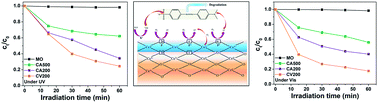
Here we report the photocatalytic activity of CeO2 nanoparticles. This is carried out with methyl orange as the reference pollutant. Annealing of ceria under vacuum generates oxygen deficient CeO2 nanoparticles with defects such as oxygen vacancies and formation of Ce3+. This is evident from the characterization results of X-ray diffraction, Raman spectroscopy, N2 adsorption–desorption and X-ray photoelectron spectroscopy. The band gap is red shifted due to the creation of intermediate energy states of Ce3+ and oxygen vacancies in the band gap. The reduced photoluminescence (PL) intensity of defective ceria indicates that the electron–hole separation is substantially enhanced by the surface trap centers. Air annealed ceria not only has relatively low surface area but also has fewer surface defects. Thus, it is expected to display less photocatalytic activity. Vacuum annealed CeO2 indeed displays better photocatalytic activity in the degradation of methyl orange under UV and visible light as compared to the air annealed samples.


1. Introduction

Semiconductor oxide nanoparticles, particularly TiO2, are active heterogeneous photocatalysts. They are widely employed in the degradation of compounds that pollute air and waste water.1,2 However, because of the wide band gap their photocatalytic activity is limited to UV part of solar radiation.1–3 Several efforts have been devoted to improve the solar photocatalytic performance of TiO2 and doping of metal and non-metal ions is one such effective method.4–7 However, dopants acting as a recombination center is a serious issue in the photocatalytic process.8,9 Recombination decreases free carrier concentration, and thereby reduces the photocatalytic efficiency of TiO2. Recently, Chen and co-workers have developed hydrogenated black coloured TiO2 nanoparticles. This TiO2 nanoparticle has a disordered surface and a narrow band gap along with remarkably enhanced photocatalytic efficiency under solar light.10 Naldoni et al. have studied the influence of Ti3+ and oxygen vacancies in the narrowing of the band gap of reduced TiO2.11 In a similar type of study, it is reported that Zn2+ and oxygen vacancies enhance the photocatalytic activity of defective ZnO nanoparticles under visible light.12

Unlike transition metal oxides such as TiO2, ZnO the photocatalytic activity of rare earth oxides is not explored to a large extent. Catalytic activity of CeO2 in the removal of air pollutants such as CO, NO are explored. The importance of CeO2 in these applications is mostly realized owing to the presence of oxygen vacancies and formation of Ce3+ on the surface.13–21 Scanning tunneling microscopy (STM), atomic force microscopy (AFM), Raman scattering, X-ray photoelectron spectroscopy (XPS) and UV-vis spectroscopic studies of ceria in the form of thin film and powder give evidences of the presence of surface, subsurface oxygen defects.16–21 Recent studies suggest that CeO2 is equally effective in the photocatalytic degradation of organic pollutants present in waste water.22–25 Khan et al. studied photodegradation of amido black and acridine orange by CeO2 nanoparticles.22 Yang et al. surveyed that mesoporous CeO2 hollow spheres with high surface area exhibited better photocatalytic activity in the degradation of Congo red than commercial CeO2.23 Ji et al. explored photocatalytic activity of mesoporous CeO2 and observed better performance in the photodegradation of acid orange 7 than that of bulk CeO2 or commercial TiO2.24 Channei et al. studied photodegradation of formic and oxalic acid by Fe doped CeO2 and observed that 2 mol% Fe doped CeO2 exhibited the best photocatalytic performance.25 Although these reports gave emphasis on the photocatalytic activity of CeO2 in water treatment, none of these reports discussed the possible role of Ce3+ and oxygen defects in the enhancement of the photocatalytic activity of CeO2.

In this article we have discussed the effect of oxygen vacancies and formation of Ce3+ on the photocatalytic activity of CeO2 nanoparticles. Role of oxygen vacancies on the photocatalytic activity of oxygen deficient TiO2 have been widely explored as mentioned in the starting of the manuscript. However, to the best of our knowledge there are hardly any reports on the photocatalytic activity of oxygen deficient CeO2 nanoparticles. Therefore, we have prepared both vacuum and air annealed CeO2 nanoparticles. Their photocatalytic activities are studied in the photodegradation of methyl orange (MO) under UV and visible light. Formation of Ce3+ and presence of oxygen vacancies are well characterized by X-ray diffraction, Raman spectroscopy, X-ray photoelectron, UV-vis spectroscopy and photoluminescence spectroscopy. From the results of these characterizations it is anticipated that Ce3+ and oxygen vacancies present on the surface of vacuum annealed CeO2 interact strongly with the surface adsorbed chromophore of methyl orange and degrades it.

2. Materials and methods

2.1 Synthesis and characterization of oxygen deficient CeO2 nanoparticles

CeO2 nanoparticles were synthesized by basic hydrolysis of cerium nitrate hexahydrate. Aqueous NH3 solution was added to 0.1 M cerium nitrate hexahydrate and stirred the mixture for 2 h. The yellow product was dried and calcined in vacuum at 200 °C (CV200) and in air at 200 °C (CA200) and 500 °C (CA500) respectively (experimental details are included in ESI). The prepared samples were successfully characterized with X-ray diffraction, transmission electron microscope (TEM), Raman spectroscopy, X-ray photoelectron spectroscopy (XPS), UV-vis spectroscopy and photoluminescence spectroscopy (PL) and the surface area was determined from the N2 adsorption–desorption isotherm (characterization details are included in electronic ESI).

2.2 Photocatalytic performance of oxygen deficient CeO2 nanoparticles

Photocatalytic activities of vacuum annealed (CV200) and air-annealed (CA200 and CA500) samples were carried out to degrade 10 mg of methyl orange (MO). Photodegradation of MO was monitored by observing the changes in the maximum absorbance of MO at 464 nm. The absorption maximum at 464 nm undergoes changes after irradiation of MO for time periods of 15, 30, 45 and 60 min. We have also studied the self degradation of catalyst free or blank MO solution. For this purpose, blank MO solution was irradiated for the above mentioned time periods and then monitored the changes in the dye concentration. Photocatalytic efficiency of oxygen deficient CV200 in the degradation of MO was also studied in the absence of light or under dark condition (photocatalytic experiment is explained in ESI).

3. Results and discussion

XRD patterns of CeO2 are shown in Fig. 1. The diffraction peaks of the samples correspond to the cubic phase of CeO2 (JCPDS 65-5923).26 Crystallite size is calculated in the Eva software equipped with the X-ray diffractometer. The software uses Scherrer's formula, d = 0.9λ/β[thin space (1/6-em)]cos[thin space (1/6-em)]θ where d is the crystallite size, λ is the wavelength of X-ray radiation and θ is the diffraction angle. The calculated crystallite sizes for CV200, CA200 and CA500 are 10 nm, 12 nm and 15 nm respectively. The small size of CV200 is due to the presence of high concentration of defects on the surface as well on the grain boundary. These defects generate a stress field in these regions and prevent growth of the nanocrystallite.27 However, calcination of CV200 in air at 200 °C (to obtain CA200) and 500 °C (to obtain CA500) progressively removes the defects from these regions and improves the crystallinity. The d-spacing of the samples are determined in the WinPLOTR software considering intense (111) peak. After obtaining d-spacing the lattice constant a for cubic CeO2 is determined. The calculated lattice constant values for CV200, CA200 and CA500 are 5.422 Å, 5.417 Å and 5.407 Å respectively. The lattice constant of the samples are higher than that of bulk ceria, which is 5.403 Å (JCPDS 65-5923). These results show that CV200 with a crystallite size of 10 nm has a lattice constant of 5.422 Å, whereas CA500 with a size of 15 nm has a lattice constant of 5.407 Å. Therefore, a size dependent variation of lattice constant is observed. In previous reports the lattice expansion of CeO2 is mostly attributed to the presence of oxygen vacancies and Ce3+ in ceria nanocrystallite.27,28 In order to explain the formation of oxygen vacancies and Ce3+ in ceria Kroger–Vink notation is adopted, which is represented by image file: c3ra44603d-t1.tif.29 In this equation OxO is O2− ion on oxygen lattice site and CexCe is Ce4+ on cerium lattice site in CeO2 lattice.image file: c3ra44603d-t2.tif is doubly charged oxygen vacancy formed on the oxygen lattice site. CeCe is Ce3+ on the cerium lattice site. Formation of image file: c3ra44603d-t3.tif in CeO2 releases two free electrons. These free electrons are captured by two lattice site Ce4+ ions and are transformed to Ce3+ ions.29 The lattice expansion of CV200 is mostly due to the presence of high concentration of Ce3+ and oxygen vacancies on the surface as well as in the bulk.30 As the size of nanoparticle decreases, the surface to volume ratio increases. As a result a large proportion of atoms reside on the surface of CV200. Moreover, since CV200 is obtained by vacuum annealing, additional defects are generated on the surface. The excess atoms and defects on the surface of CV200 nanocrystallite generate tremendous lattice strain. The strain is minimized when CV200 undergoes lattice expansion.31 Calcination of CV200 in air at 200 °C (to obtain CA200) and 500 °C (to obtain CA500) increases the crystallite size and progressively decreases the amount of Ce3+ and oxygen vacancies from the surface. Increase in size and removal of Ce3+ and oxygen defects from surface minimizes the lattice strain in CA200 and CA500, resulting in the decrease in the magnitude of their lattice constant.
image file: c3ra44603d-f1.tif
Fig. 1 X-ray diffraction patterns of vacuum (CV) and air annealed (CA) CeO2 nanoparticles CV200, CA200 and CA500 respectively.

HRTEM images of the prepared nanoparticles are shown in Fig. 2a–d. The nanoparticles are not monodisperse and agglomeration persists in both CV200 and CA200. The inset of Fig. 2a and b shows the particle size distribution of CV200 and CA200. CV200 has an average size of 11 nm, whereas the average diameter of the nanoparticles becomes 13 nm in CA200. The size of the nanoparticles becomes 17 nm in CA500 (Fig. 2c). Therefore, increase in the nanoparticle size of CA200 and CA500 is due to the grain growth of the nanoparticles at 200 °C and 500 °C. The clear lattice planes of CV200 are shown in Fig. 2d. The arrows in the circular area and on other region of the image show the interface region where the nearest nanoparticles overlap each other. The enlarged view of the circular region is shown in the inset of Fig. 2d. The interface and the grain boundary are the active regions in CeO2 for the formation of Ce3+ and oxygen vacancies. Possibility of defect formation near grain boundary depends on the local atomic structure and orientation of the grains near the grain boundary. At the adjoint of the nanoparticles the lattice planes are slightly misaligned. This misalignment of lattice planes may generate line defects, containing oxygen vacancies as one of the point defects. This is an assumption that defects may be located in these regions. However, a clear visibility of the defects in this region requires very high resolution TEM or a scanning transmission electron microscope (STEM). Hojo et al. studied the grain boundary structure of CeO2 with scanning transmission electron microscope (STEM) using high angle annular dark field (HAADF) and observed the presence of Ce3+ and oxygen vacancies near the grain boundary regions.32


image file: c3ra44603d-f2.tif
Fig. 2 High resolution transmission electron microscope (HRTEM) images of CeO2 nanoparticles annealed in vacuum (a) CV200 and air (b) CA200 and (c) CA500. (d) HRTEM image of CV200 showing the lattice planes. The yellow circle shows the adjoint areas of two or more adjacent CeO2 nanoparticles. The green arrows show the regions where the lattice planes of two nanoparticles are differently aligned. Inset figure depicts the enlarged view of the circle region of the image showing the lattice planes at the interface of adjacent CeO2 nanoparticles.

N2 adsorption–desorption isotherms of CV200, CA200 and CA500 are displayed in Fig. 3a–c. The typical hysteresis behavior of the isotherms verifies their mesoporous structure.33 Surface area of the samples is determined using multipoint Brunauer–Emmett–Teller (BET) method. Fig. 3d–f presents the BJH pore size distribution profiles from which the average pore size is determined for each sample. The surface area, average pore diameter and pore volume of the samples are inserted in Table 1. CV200 has the highest surface area (113 m2 g−1), whereas CA500 exhibits the lowest surface area (63.6 m2 g−1). The pore diameters of the samples are within the range of 2–50 nm. This is the characteristic dimension range of mesoporous materials as specified by IUPAC recommendation.34


image file: c3ra44603d-f3.tif
Fig. 3 N2 adsorption–desorption isotherms for (a) CV200 (b) CA200 and (c) CA500. Pore size is determined using BJH method for (d) CV200 (e) CA200 and (f) CA500.
Table 1 BET surface area, pore size, pore volume, photodegradation and rate constant of CV200, CA200 and CA500
Sample Surface area (m2 g−1) Pore size (nm) Pore volume (cm3 g−1) % Photodegradation Rate constant (min−1)
UV Vis UV Vis
CV200 113.07 5.199 0.171 75.50 82.30 0.0230 0.0268
CA200 86.10 5.689 0.146 65.66 59.73 0.0168 0.0145
CA500 63.60 8.154 0.140 44.04 37.10 0.0080 0.0073


Fig. 4a shows the core level Ce 3d XPS spectrum of CV200. The XPS spectrum is deconvoluted into 10 Gaussian peaks with the labels following the convolution of Burroughs et al.35 The labels U, U′′, U′′′, V, V′′ and V′′′ refer to Ce 3d3/2 and Ce 3d5/2 and are characteristic peaks of Ce4+ in CeO2.36–38 The highest binding energy (BE) peaks U′′′ and V′′′ are located at 916.9 eV and 898.2 eV and arise from Ce (3d94f0) O (2p6) final state. The lower BE states U′′ and V′′ are located at 907.5 eV and 888.95 eV and are assigned to Ce (3d94f1) O (2p5). The BE peaks of U and V at 901.1 eV and 881.89 eV are result of Ce (3d94f2) O (2p4) final state. In case of Ce 3d of Ce3+, BE peaks of Ce 3d consists of two pair of doublets (U0, V0, U′ and V′).37 For Ce3+ the highest BE peaks U′ and V′ appear at 903.4 eV and 885.02 eV respectively.38 These doublets correspond to Ce (3d94f1) O (2p5). The lowest BE peaks U0 and V0 occurs at 880.2 eV and 898.2 eV and correspond to Ce (3d94f1) O(2p6). Fig. 4b shows the core level XPS spectrum of O 1s. The BE peak A at 529.6 eV is due to lattice O2− ion attached to Ce4+ ion, whereas the peak B at 531.7 eV is due to adsorbed oxygen to Ce3+ site.38–40 The 1s electrons in oxygen are more tightly attached to Ce3+ than to Ce4+.39,40 The peak B is broader than A which is due to the different coordination of oxygen ion to Ce3+ in oxygen deficient CV200.39


image file: c3ra44603d-f4.tif
Fig. 4 (a) Core level X-ray photoelectron (XPS) spectrum of Ce 3d3/2,5/2 for CV200 nanoparticles. The spectrum is deconvoluted into 10 Gaussian peaks. (b) Core level O 1s XPS spectrum is deconvoluted into two Gaussian peaks.

Raman spectroscopy is carried out to understand the defect induced changes in the local structure of CeO2 nanoparticles. Fig. 5 displays the Raman spectra of CV200, CA200 and CA500. The intense signal of CV200 at 444 cm−1 is assigned to the F2g mode of ceria.41 F2g mode of bulk CeO2 appears at 464 cm−1.42,43 This F2g signal is due to the breathing mode of oxygen in the Ce–O8 vibrational unit and is assigned to second order transverse acoustic mode (2TA).42,43 It is observed that the position of F2g signal of CV200 is red shifted from that of the position of bulk CeO2. It is speculated that both nanocrystallite size and structural defects affect the position of the F2g mode in CV200. In case of pure crystal the Raman scattering comes from the center of the Brillouin zone by satisfying the phonon selection rule, k = 0.43 This selection rule is not valid in nanocrystalline materials due to strong phonon confinement. Therefore, phonon contribution comes from entire Brillouin zone resulting in the shifting of the Raman peak position. Defects, such as oxygen vacancies, also disrupt the Ce–O vibrational unit and as an outcome the F2g mode undergoes red shifting.43,44 Crystallite size increases and the structural defects diminishes in CA200 and CA500, resulting in the progressive shifting of the Raman F2g signal to 458 cm−1 and 460 cm−1 respectively. Apart from the F2g peak, the Raman spectrum of CV200 exhibits three additional peaks at 242 cm−1, 588 cm−1 and 1174 cm−1 respectively. Weak mode at 242 cm−1 corresponds to doubly degenerate transverse optical mode (2TO) and the intense mode at 588 cm−1 is attributed to non-degenerate longitudinal optical (LO) mode. This LO mode is associated with intrinsic oxygen defects present in ceria lattice.41–45 The Raman signal at 1174 cm−1 is the doubly degenerate longitudinal optical (2LO) mode. This mode is associated with the O–O stretching vibration mode of surface adsorbed superoxide anion (O2˙).44,45 The enlarged view of 2LO mode can be seen in the inset of Fig. 5. The intensity of this mode decreases in CA200 and nearly disappears in CA500. This superoxide radical is formed by the interaction of the surface adsorbed oxygen with the electron trapped in the oxygen vacancy. Therefore, disappearance of 2LO mode also indicates absence of surface oxygen defects.


image file: c3ra44603d-f5.tif
Fig. 5 Raman spectra of CV200, CA200 and CA500 respectively. Inset shows the enlarged view of the 2LO mode at 1174 cm−1. The peak intensity is intense in CV200 but diminishes in CA200 and nearly disappears in CA500.

Kubelka–Munk (K–M) absorption spectra of CV200, CA200 and CA500 are shown in Fig. 6a. The corresponding reflectance spectra of the samples are shown in Fig. 6b. The conversion of reflectance to K–M absorption follows the equation F(R) = (1 − R)2/2R, where R is the reflectance and F(R) is the K–M absorption. The maximum absorption peak at 320 nm is assigned to the charge transfer transition from O2− in O 2p to Ce4+ in Ce 4f.46,47 As shown in Fig. 6a, the colour of CV200 is black, whereas CA200 has light brown and CA500 has light yellowish colour. CV200 contains an absorption tail extending to the visible region, which is otherwise absent in CA200 and CA500. The black colour and the extended absorption tail in CV200 are due to the presence of large concentration of Ce3+ and oxygen vacancies. The single 4f1 electron in Ce3+ undergoes 4f1–5d transition and gives absorption at ∼420 nm. Photoexcitation of the trapped electrons in the oxygen vacancy to the conduction band may also give absorptions in the visible region. The band gap of the samples are determined by plotting [F(R)]1/n vs. hυ (n = 2 for indirect band gap).48 A straight line is drawn on the linear part of the curves, which on extrapolation on the X-axis gives the band gap (Fig. 6c). The reported indirect band gap of bulk ceria is in the range between 3.0 and 3.2 eV.49,50 The band gap of CV200, CA200 and CA500 are 2.49 eV, 2.87 eV and 2.92 eV respectively. The narrowing in the band gap may be associated with oxygen vacancies and formation of Ce3+. Oxygen vacancies and Ce3+ forms intermediate defect energy states in the band gap of CeO2. Because of the presence of these states the direct transition of electrons from O 2p to Ce 4f is retarded, resulting in the narrowing in the band gap. These results arrive at a conclusion that defects have direct influence on the band gap of the samples. Higher is the concentration of these defects, larger will be the reduction in the band gap and vice versa.


image file: c3ra44603d-f6.tif
Fig. 6 (a) Kubelka–Munk absorption plot for oxygen deficient black CV200, brownish CA200 and yellowish CA500. The absorption edge is slightly extended towards visible region in CV200 indicating the presence of localized defect energy states in the band gap. (b) Reflectance spectra of CV200, CA200 and CA500. (c) Plot of [F(R)]1/2 vs. hυ for the determination of band gap of vacuum (CV200) as well as air annealed (CA200 and CA500) CeO2 nanoparticles.

Photoluminescence (PL) is an important spectroscopic technique to evaluate the role of crystalline defects on the carrier recombination process in a material. Fig. 7 shows the PL spectra of CeO2 excited at 320 nm. In order to distinguish the different emission peaks, one of the emission spectrum is fitted with Gaussian function with a correctness of fitting, r2 = 0.9986. The UV emission peak at 390 nm is due to the indirect transition of electrons from Ce 4f level to O 2p level. The visible emission peaks lying in between 428 and 539 nm are mostly associated with oxygen vacancies with trapped electrons, such as F+ (oxygen vacancy with one trapped electron), F2+ (oxygen vacancy without any electrons) and F (oxygen vacancy with two trapped electrons).47,49,51 The intensities of UV and visible emission peaks are suppressed in CV200, whereas the intensities are tremendously enhanced in CA200 and CA500. The efficiency of a PL emission is affected by both radiative and non-radiative defects present in the bulk as well as on the surface. It is believed that bulk defects act as radiative charge carrier recombination centers, and therefore enhance the PL emission. On the other hand surface defects act as non-radiative trap centers.52 CV200 contains high density of oxygen vacancies and Ce3+ trap centers on the surface as well as on the grain boundary. These trap centers act as non-radiative recombination centers and suppress the emission intensity of CV200. However, the numbers of these non-radiative centers are likely to be less in the air annealed CA200 and CA500. Under these circumstances, the photoexcited electrons and holes easily recombine in the bulk as well as on the surface of CA200 and CA500, resulting in the enhancement of emission intensity.


image file: c3ra44603d-f7.tif
Fig. 7 Room temperature photoluminescence (PL) spectrum of CV200, CA200 and CA500 obtained at an excitation wavelength of 320 nm. Deconvolution of the emission spectrum of CV200 into five Gaussian peaks.

3.1 Photocatalytic activity study

From the results of XRD, XPS, Raman, UV-vis and PL it is clear that Ce3+ and oxygen vacancies are considerably higher in CV200 than in CA200 or CA500. These defects are responsible for the narrowing of band gap and for the large separation of surface charge carriers in CV200. The band gap widens and carrier recombination increases because of the decrease in the density of surface defects in CA200 and CA500. The BET surface area of CV200 is also higher than CA200 and CA500. Therefore, from these observations it is manifested that high surface area, narrow band gap and availability of free charge carriers make CV200 a useful material for UV as well as for visible light photocatalysis. Fig. 8a and b displays the absorption curves of CV200 catalyzed MO solution after irradiation under UV and visible light. The irradiation time periods were 15, 30, 45 and 60 min respectively. Irradiation results in the decrease in the initial concentration of the dye solution. Fig. 9a and b shows the decrease in the dye concentration (Ct/C0) with increase in irradiation time. The photodegradation of MO by CV200 is studied under dark condition (Fig. S1, ESI). The MO solution, loaded with CV200, is stirred for 60 min under dark (without turning on any UV or visible light). During stirring the MO solution is likely to be adsorbed on every active facets of CV200. However, it is seen that there is negligible decrease in the concentration of MO solution. Under dark condition, only the freely available carriers on the surface of CV200 take part in the degradation of MO. Since the numbers of these carriers is very less, the degradation of MO is also very slow under dark.
image file: c3ra44603d-f8.tif
Fig. 8 Absorption curves of MO solution catalyzed by CV200. The maximum absorption peak at 464 nm gradually decreases when CV200 catalyzed MO solutions are irradiated under (a) UV and (b) visible light.

image file: c3ra44603d-f9.tif
Fig. 9 Plot of Ct/C0 vs. irradiation time (t) showing a decrease in the initial concentration of MO with irradiation time in presence of the catalysts CV200, CA200 and CA500 under (a) UV and (b) visible light.

In comparison to simple stirring under dark condition, the decrease in the initial concentration of MO is much faster when UV or visible light is turned on. The initial concentration of MO decreases to minimum in the presence of the catalyst. On the other hand, there is hardly any change in the concentration of MO when it is irradiated in the absence of catalyst. Table 1 displays the maximum degradation of MO by CV200, CA200 and CA500 under UV and visible light. As shown in Table 1, blank MO in the absence of catalyst exhibit negligible degradation. Blank MO solution degrades only by 2% under UV and visible light. CV200 shows the maximum degradation of 75.5% under UV light and 82.3% under visible light. The efficiency of the catalyst decreases with decrease in the surface area and defect content, which can be seen in case of CA200 and CA500 in Table 1. The photodecomposition of MO in absence and in presence of ceria fits the pseudo first order rate equation ln(Ct/C0) = kt where t is the irradiation time and k is the apparent rate constant. The plot of ln(Ct/C0) vs. t follows a linear relation with the rate constant determined from the slope of the linear fitting (Fig. 10a and b). The rate constant of the photocatalytic degradation of MO, in the absence of catalyst, is 0.0026 min−1 and 0.0021 min−1 under UV and visible light. The rate constant values of CV200, CA200 and CA500 are incorporated in Table 1. As Table 1 shows CV200 has the highest rate constant under UV (0.0230 min−1) and visible light (0.0268 min−1). On the other hand, the rate of the photocatalytic degradation decreases in CA200 (0.0168 min−1 under UV and 0.0145 min−1) and CA500 (0.0080 min−1 under UV and 0.0073 min−1) respectively.


image file: c3ra44603d-f10.tif
Fig. 10 Plot of ln(Ct/C0) vs. irradiation time (t) showing the first order kinetics in the degradation of MO by CV200, CA200 and CA500 under (a) UV and (b) visible light irradiation.

Mechanism of photocatalysis

Illuminating a solid with UV/vis light excites electrons to the conduction band leaving holes in the valence band. During photoexcitation few electrons move to the conduction band, while the rest of the excited electrons are trapped in the oxygen vacancies present below Ce 4f level. The electrons present in the conduction band and in the trap states migrate to the surface and got captured by the surface oxygen vacancies. Atmospheric O2 molecules adsorbed on the surface oxygen vacancies are transformed into superoxide radicals (O2˙). During discussion on Raman spectroscopy we stated that superoxide radicals are initially present on the surface of CeO2 (1174 cm−1 peak). Additional superoxide ions are formed when the catalyst is irradiated in presence of dye solution. The oxygen molecules (present in dissolved forms in MO solution) interact with the surface oxygen vacancies and are transformed into superoxide radicals. Similarly, holes are captured by H2O or OH groups forming hydroxyl radicals (˙OH). These superoxide and hydroxyl radicals finally degrade the dye.

In nanocrystalline CV200 an amorphous Ce2O3 surface layer (with Ce3+ and oxygen vacancies) covers the CeO2 core. The thickness of the Ce2O3 layer depends on the size of the nanocrystallite and concentration of Ce3+ and oxygen vacancies on the surface. Fig. 11 shows a schematic representation of the interaction of the functional groups of MO with the active Ce3+ and oxygen vacancies present in Ce2O3 layer. During photocatalytic reaction the dye is first adsorbed on the Ce2O3 layer and then adsorbed through this surface layer and moves into the core. In this process, few of the adsorbed O2 molecules interact with the surface Ce3+ and oxygen vacancies, and the rest of the O2 molecules migrate into the lattice interior and fill up the vacant oxygen spaces. The holes present on the surface interact with water and hydroxide ions. Now, the various surface active agents in CV200 are oxygen vacancies with trapped electrons (F, F+, F2+) and Ce3+ ions. Since F centers have two electrons, these electrons are transferred to two molecules of surface adsorbed oxygen to form superoxide radicals (O2˙), F+ (one trapped electron) and F2+ (no trapped electrons) centers respectively. Ce3+ has one electron in the 4f orbital and this electron is transferred to adsorbed oxygen to form superoxide radical, whereas holes interact with water to form hydroxyl radical. The superoxide radical may interact with proton (H+) to form hydroperoxyl (HO2˙) radical. The hydroperoxy radical takes electron and proton to form hydrogen peroxide, which finally forms hydroxyl radical by capturing one electron. These superoxide and hydroxyl radicals interact with the dye and finally degrade it. The above mentioned steps of photoexcitation, generation of radicals and dye degradation are summarized below.

CeO2 + → h+ + e

e + h+ → energy

O2(ads) + F → O2˙ + F+

O2(ads) + F+ → O2˙ + F2+

Ce4+ + e → Ce3+

Ce3+ + O2(ads) → Ce4+ + O2˙

H2O + h+ → ˙OH + H+

O2˙ + H+ → HO2˙

HO2˙ + e + H+ → H2O2

H2O2 + e → OH˙ + OH

O2˙ + MO → Degradation

OH˙ + MO → Degradation


image file: c3ra44603d-f11.tif
Fig. 11 Schematic diagram of the photocatalytic processes taking place on the surface of CeO2. The topmost blue region (1a) is Ce2O3 layer containing Ce3+ and oxygen vacancies with trapped electrons (F, F+) and the yellow region is CeO2 core (1b). The two electrons in F centers are transformed to two molecules of oxygen forming 2 molecules of superoxide radicals (O2˙) (2a), whereas the lone trapped electron in F+ center interact with single oxygen molecule forming single superoxide ion (2b and 2c). The single 4f1 electron in Ce3+ also interacts with O2 forming superoxide radical (3). The hole (h+) on the surface is transformed to water molecule to form hydroxyl radicals (˙OH) (4). Ultimately the hydroxyl radical (5a) and superoxide radical (5b) brings about degradation of MO.

These photocatalytic reactions take place very efficiently on the surface of CV200. The high surface area of CV200 carriers a large numbers of superoxide and hydroxyl radicals. These radicals interact strongly with the surface adsorbed MO and as a result MO undergoes degradation. In case of air annealed CA200 many of the surface oxygen vacancies are filled up and the concentration of Ce3+ decreases on the surface. This results in the decrease in the thickness of Ce2O3 layer. Since thickness decreases, the surface adsorbed O2 molecule easily penetrates the Ce2O3 layer and moves into the core. Therefore, the numbers trap centers and adsorbed O2 molecule both decreases on the surface of CA200. The final outcome is the reduction in the numbers of superoxide and hydroxyl radicals on the surface of CA200, and hence decreases in the photodegradation of MO. Air annealed CA500 not only has low surface area but also has less surface defects. Due to the reduction in the surface trap centers the electrons and holes easily recombine on the surface. Unavailability of trap centers and free surface charge carriers reduces the numbers of superoxide and hydroxyl radicals on the surface of CA500. Thus, CA500 exhibit the least catalytic efficiency in the degradation of MO under UV and visible light.

4. Conclusion

In summary, we studied the effect of Ce3+ and oxygen vacancies on the photocatalytic activity of oxygen deficient CeO2. Annealing of ceria under vacuum introduces formation of Ce3+ and oxygen vacancies on the lattice site, surface and grain boundary. These trap states not only extend the absorption edge of CeO2 but also separate the carriers from recombination. The prepared oxygen deficient CV200 has high surface area, narrow band gap and large concentration of free electron and holes on the surface. This catalyst degrades 82.3% of the methyl orange under visible light with a rate constant of 0.0268 cm−1. Removal of these defects by air annealing reduces the surface area, increases the band gap and reduces the numbers of free electron and holes. CA200 degrades 59.73% of MO under visible light with rate kinetics of 0.0145 min−1. CA500 has the least catalytic efficiency and degrades only 37.1% under visible light with first order rate constant of 0.0073 cm−1. Hence, the inference that can be drawn from these observations is that defective CeO2, without any dopant, may show good photocatalytic activity provided the samples contain enough surface defects and exhibit high surface area.

Acknowledgements

Author1 and Author3 acknowledge the financial support provided by Department of Science and Technology (DST), India, to the project SR/NM/NS-98/2010 (G) and Author2 likes to acknowledge DST, Govt. of India for providing the Inspire Fellowship.

References

  1. A. L. Linsebigler, G. Lu and J. T. Yates, Chem. Rev., 1995, 95, 735–758 CrossRef CAS.
  2. H. Taoda, Res. Chem. Intermed., 2008, 34, 417–428 CrossRef CAS PubMed.
  3. K. Hashimoto, H. Irie and A. Fujishima, Jpn. J. Appl. Phys., 2005, 44, 8269–8285 CrossRef CAS.
  4. F. Zuo, K. Bozhilov, R. J. Dillon, L. Wang, P. Smith, X. Zhao, C. Bardeen and P. Feng, Angew. Chem., Int. Ed., 2012, 51, 6223–6226 CrossRef CAS PubMed.
  5. G. Colon, M. Maicu, M. C. Hidalgo and J. A. Navio, Appl. Catal., B, 2006, 67, 41–51 CrossRef CAS PubMed.
  6. N. Umezawa and J. Ye, Phys. Chem. Chem. Phys., 2012, 14, 5924–5934 RSC.
  7. J. Yu, G. Dai, Q. Xiang and M. Jaroniec, J. Mater. Chem., 2011, 21, 1049–1057 RSC.
  8. B. Choudhury, B. Borah and A. Choudhury, Photochem. Photobiol., 2012, 88, 257–264 CrossRef CAS PubMed.
  9. W. Choi, A. Termin and M. R. Hoffmann, J. Phys. Chem., 1994, 98, 13669–13679 CrossRef.
  10. X. Chen, L. Liu, P. Y. Yu and S. S. Mao, Science, 2011, 331, 746–750 CrossRef CAS PubMed.
  11. A. Naldoni, M. Allieta, S. Santangelo, M. Marelli, F. Fabbri, S. Cappelli, C. L. Bianchi, R. Psaro and V. D. Santo, J. Am. Chem. Soc., 2012, 134, 7600–7603 CrossRef CAS PubMed.
  12. F. Liu, Y. H. Leung, A. B. Djurisic, A. M. C. Ng and W. K. Chan, J. Phys. Chem. C, 2013, 117, 12218–12228 CAS.
  13. Y. Kang, M. Sun and A. Li, Catal. Lett., 2012, 142, 1498–1504 CrossRef CAS.
  14. A. Trovarelli, Catal. Rev.: Sci. Eng., 1996, 38, 439–520 CAS.
  15. S. Wenjuan, G. Hongjuan, L. Chang and W. Xiaonan, J. Rare Earths, 2012, 30, 665–669 CrossRef.
  16. J.-L. Lu, H.-J. Gao, S. Shaikhutdinov and H. J. Freund, Surf. Sci., 2006, 600, 5004–5010 CrossRef CAS PubMed.
  17. D. C. Grinter, R. Ithnin, C. L. Pang and G. Thornton, J. Phys. Chem. C, 2010, 114, 17036–17041 CAS.
  18. S. Torbrugge and M. Reichling, Phys. Rev. Lett., 2007, 99, 056101 CrossRef.
  19. F. Vindigni, M. Manzoli, A. Damin, T. Tabakova and A. Zecchina, Chem.–Eur. J., 2011, 17, 4356–4361 CrossRef CAS PubMed.
  20. J. P. Holgado, R. Alvarez and G. Munuera, Appl. Surf. Sci., 2000, 161, 301–315 CrossRef CAS.
  21. P. Patsalas, S. Logothetidis, L. Sygellou and S. Kennou, Phys. Rev. B: Condens. Matter Mater. Phys., 2003, 68, 035104 CrossRef.
  22. S. B. Khan, M. Faisala, M. M. Rahmana and A. Jamala, Sci. Total Environ., 2011, 409, 2987–2992 CrossRef CAS PubMed.
  23. Z. Yang, J. Wei, H. Yang, L. Liu, H. Liang and Y. Yang, Eur. J. Inorg. Chem., 2010, 2010, 3354–3359 CrossRef.
  24. P. Ji, J. Zhang, F. Chen and M. Anpo, J. Phys. Chem. C, 2008, 112, 17809–17813 CAS.
  25. D. Channei, B. Inceesungvorn, N. Wetchakun, S. Phanichphant, A. Nakaruk, P. Koshy and C. C. Sorrell, Ceram. Int., 2013, 39, 3129–3134 CrossRef CAS PubMed.
  26. B. Choudhury and A. Choudhury, Mater. Chem. Phys., 2012, 131, 666–671 CrossRef CAS PubMed.
  27. S. Deshpande, S. Patil, S. Kuchibhatla and S. Seal, Appl. Phys. Lett., 2005, 87, 133113 CrossRef PubMed.
  28. L. Wu, H. J. Wiesmann, A. R. Moodenbaugh, R. F. Klie, Y. Zhu, D. O. Welch and M. Suenaga, Phys. Rev. B: Condens. Matter Mater. Phys., 2004, 69, 125415 CrossRef.
  29. M. Nolana, J. E. Fearon and G. W. Watson, Solid State Ionics, 2006, 177, 3069–3074 CrossRef PubMed.
  30. S. Tsunekawa, S. Ito and Y. Kawazoe, Appl. Phys. Lett., 2004, 85, 3845–3847 CrossRef CAS PubMed.
  31. S. Tsunekawa, K. Ishikawa, Z. Q. Li, Y. Kawazoe and A. Kasuya, Phys. Rev. Lett., 2000, 85, 3440–3443 CrossRef CAS.
  32. H. Hojo, T. Mizoguchi, H. Ohta, S. D. Findlay, N. Shibata, T. Yamamoto and Y. Ikuhara, Nano Lett., 2010, 10, 4668–4672 CrossRef CAS PubMed.
  33. C. G. Sonwane and S. K. Bhatia, J. Phys. Chem. B, 2000, 104, 9099–9110 CrossRef CAS.
  34. J. Rouquerol, D. Avnir, C. W. Fairbridge, D. H. Evertt, J. H. Haynes, N. Pernicone, J. D. Ramsay, K. S. W. Sing and K. K. Unger, Pure Appl. Chem., 1994, 66, 1739 CrossRef CAS.
  35. P. Burroughs, A. Hamnett, A. F. Orchard and G. Thornton, J. Chem. Soc., Dalton Trans., 1976, 17, 1686–1698 RSC.
  36. V. Fernandes, P. Schio, A. de Oliveira, W. A. Ortiz, P. Fichtner, L. Amaral, I. L. Graff, J. Varalda, N. Mattoso, W. H. Schreiner and D. H. Mosca, J. Phys.: Condens. Matter, 2010, 22, 216004 CrossRef CAS PubMed.
  37. L. R. Shah, B. Ali, H. Zhu, W. G. Wang, Y. Q. Song, H. W. Zhang, S. I. Shah and J. Q. Xiao, J. Phys.: Condens. Matter, 2009, 21, 486004 CrossRef PubMed.
  38. P. Charvin, D. Perarnau, S. Abanades and G. Flamant, Surf. Interface Anal., 2008, 40, 264–267 CrossRef.
  39. V. Fernandes, P. Schio, A. Oliveira, W. H. Schreiner, J. Varalda and D. H. Mosca, J. Appl. Phys., 2011, 110, 113902 CrossRef PubMed.
  40. Y. Q. Song, H. W. Zhang, Q. Y. Wen, L. Peng and J. Q. Xiao, J. Phys.: Condens. Matter, 2008, 20, 255210 CrossRef.
  41. J. E. Spanier, R. D. Robinson, F. Zhang, S. W. Chan and I. P. Herman, Phys. Rev. B: Condens. Matter Mater. Phys., 2001, 64, 245407 CrossRef.
  42. Z. Wu, M. Li, J. Howe, H. M. Meyer and S. H. Overbury, Langmuir, 2010, 26, 16595–16606 CrossRef CAS PubMed.
  43. I. Kosacki, T. Suzuki, H. U. Anderson and P. Colomban, Solid State Ionics, 2002, 149, 99–105 CAS.
  44. S. Askrabic, Z. D. Mitrovic, A. Kremenovic, N. Lazarevic, V. Kahlenberg and Z. V. Popovic, J. Raman Spectrosc., 2012, 43, 76–81 CrossRef CAS.
  45. T. Taniguchi, T. Watanabe, N. Sugiyama, A. K. Subramani, H. Wagata, N. Matsushita and M. Yoshimura, J. Phys. Chem. C, 2009, 113, 19789–19793 CAS.
  46. C. Ho, J. C. Yu, T. Kwong, A. C. Mak and S. Lai, Chem. Mater., 2005, 17, 4514–4522 CrossRef CAS.
  47. B. Choudhury, P. Chetri and A. Choudhury, J. Exp. Nanosci., 2013 DOI:10.1080/17458080.2013.801566.
  48. J. Strunk, W. C. Vining and A. T. Bell, J. Phys. Chem. C, 2011, 115, 4114–4126 CAS.
  49. V. Ptrovsky, B. P. Gorman, H. U. Anderson and T. Petrovsky, J. Appl. Phys., 2001, 90, 2517 CrossRef PubMed.
  50. J. C. Nie, Z. Y. Hua, R. F. Dou and Q. Y. Tu, J. Appl. Phys., 2008, 103, 054308 CrossRef PubMed.
  51. A. H. Morshed, Appl. Phys. Lett., 1997, 70, 1647–1649 CrossRef CAS PubMed.
  52. Y. Li, X. Chen, T. Tian, P. Fang, F. Zhang and X. Zhao, J. Am. Chem. Soc., 2011, 133, 16414–16417 CrossRef PubMed.

Footnote

Electronic supplementary information (ESI) available. See DOI: 10.1039/c3ra44603d

This journal is © The Royal Society of Chemistry 2014
Click here to see how this site uses Cookies. View our privacy policy here.