 Open Access Article
 This Open Access Article is licensed under a
 Creative Commons Attribution 3.0 Unported Licence
Tantalum-oxide catalysed chemical vapour deposition of single- and multi-walled carbon nanotubes†
Bernhard C.
Bayer
*a,
Carla
Castellarin-Cudia
bc,
Raoul
Blume
d,
Stephen A.
Steiner
III
e,
Caterina
Ducati
f,
Daping
Chu
a,
Andrea
Goldoni
c,
Axel
Knop-Gericke
g,
Robert
Schlögl
g,
Cinzia
Cepek
b,
John
Robertson
a and
Stephan
Hofmann
a
aDepartment of Engineering, University of Cambridge, Cambridge, CB3 0FA, UK. E-mail: bcb25@cam.ac.uk; Fax: +44 (0)1223/748348; Tel: +44 (0)1223/748291
bIstituto Officina dei Materiali-CNR, Laboratorio TASC, I-34149 Trieste, Italy
cSincrotrone Trieste SCpA, I-34149 Trieste, Italy
dHelmholtz-Zentrum Berlin für Materialien und Energie, D-12489 Berlin, Germany
eDepartment of Aeronautics and Astronautics, Massachusetts Institute of Technology, Cambridge, MA 02139, USA
fDepartment of Materials Science and Metallurgy, University of Cambridge, Cambridge, CB2 3QZ, UK
gFritz-Haber-Institut der Max-Planck-Gesellschaft, D-14195 Berlin-Dahlem, Germany
First published on 16th January 2013
Abstract
Tantalum-oxide thin films are shown to catalyse single- and multi-walled carbon nanotube growth by chemical vapour deposition. A low film thickness, the nature of the support material (best results with SiO2) and an atmospheric process gas pressure are of key importance for successful nanotube nucleation. Strong material interactions, such as silicide formation, inhibit nanotube growth. In situ X-ray photoelectron spectroscopy indicates that no catalyst reduction to Ta-metal or Ta-carbide occurs during our nanotube growth conditions and that the catalytically active phase is the Ta-oxide phase. Such a reduction-free oxide catalyst can be technologically advantageous.
1. Introduction
Chemical vapour deposition (CVD) of carbon nanotubes (CNTs) involves the decomposition of gaseous carbon precursors over a nanoparticle catalyst and subsequent incorporation of the carbon into the growing nanotube structure.1 To date, the most extensively studied “standard” catalyst materials are metallic Fe, Ni and Co.2–4 However, recently a range of other catalyst materials has been shown to nucleate CNTs by CVD as well. These include “non-standard” metals,5–9 semiconductor nanoparticles,10,11 nanostructured carbon materials12–14 and oxide nanoparticles.15–26 Likewise, first attempts at oxide-catalysed graphene CVD have recently been made.27,28This gradually expanding plurality of catalyst materials for CNT CVD has challenged many previously accepted aspects of the CNT growth model2,29 such as the need for a transition metal catalyst, the need for a balanced finite carbon solubility in the catalyst30 and the need for a balance in the metal–carbon valence orbital overlap.9 Fundamentally, it remains unclear as to what extent various catalyst nanoparticles serve as chemical catalysts that lower reaction barriers and/or as geometrical seeding templates for nanotube cap formation.31
Oxide catalysts in particular are puzzling: Refractory metal-oxides have been widely used as supports for standard metal catalysts in CNT growth but had previously generally been considered to be chemically inert towards nanotube formation. We however showed that hard-to-reduce ZrO2 nanoparticles facilitate nanotube growth without reduction of the zirconia at any stage during the CVD process.20In situ X-ray photoelectron spectroscopy (XPS) suggested that chemically active, substoichiometric (surface) defects on the otherwise inert oxide promote CNT nucleation.20 Likewise, for the technologically important oxide catalyst SiOx there is currently an intense debate whether the nanoparticles facilitating CNT growth remain as an oxide,21 form surface defects,22 reduce to SiC on the surface,24 reduce to SiC entirely in the bulk23 or are even liquid19 during CVD.
Similar to Si and Zr, tantalum (Ta) can form stable compounds with C, O, H or N, respectively,32,33 which are all common elements in nanotube CVD process gases. In particular, Ta is (similar to Si) a slightly weaker oxide former than Zr but Ta is (similar to Zr) a stronger carbide former than Si.34 These properties suggest Ta-oxide as an interesting model system to further examine the growth mechanism(s) of CNTs from non-standard catalysts.
Ta-based catalysts have not been previously used to nucleate CNTs but Ta can promote graphitisation of carbon35,36 and was reported as a catalyst for BN nanotube37 and GaN38 and SnOx39 nanowire growth. However the state of the Ta in these reactions remains unclear. Ta-oxides40-42 and Ta-carbides43–45 are well known catalysts for various heterogeneous catalytic processes. Because of their compatibility with ultra-large-scale-integration (ULSI) manufacturing, metallic Ta thin films have been previously studied as an electrically conductive support material for CNT growth employing standard catalysts34,46 and Ta has been investigated as an admixture component in FeTa CNT co-catalysts.47 Ta and its oxides and carbides are non-ferromagnetic,48,49 making Ta-based CNT catalysts appealing for magneto-electronic CNT devices. Ta-oxides (Ta2O5) are also of high technological importance (e.g., high-k dielectrics and optical coatings).50
Here, we demonstrate that Ta-oxide catalyses the growth of single-walled nanotubes (SWNTs) and multi-walled nanotubes (MWNTs). MWNT growth from Ta-oxide thin films (<1 nm) on SiO2-covered wafers can be achieved at moderate temperatures as low as ∼650 °C. This is in contrast to a large fraction of other “non-standard” CNT growth catalysts which can only nucleate SWNTs and work only at high temperatures above 900 °C. Our in situ XPS characterisation data suggests that Ta-oxides are the catalytically active phase for our CVD conditions, i.e., no reduction to Ta-metal or to Ta-carbide occurs. Such oxide catalysts are particularly promising for CNT growth on reactive substrates such as carbon fibres.20,51 Likewise, such reduction-free oxide catalysts may be technologically advantageous for integration of CNTs into electronics since the oxide materials are non-ferromagnetic, show limited reactivity with functional substrates and are already widely used in microelectronics fabrication processes.
2. Experimental methods
Metallic Ta thin films were sputter deposited onto Si wafers covered with SiO2 (200 nm), Al2O3 (10 nm on top of 200 nm SiO2), or native oxide (∼2 nm SiO2). Samples were then exposed to ambient air (minimum of 24 h) which is known to lead to oxidation of Ta films up to a thickness of 8 nm.33,52 As-formed Ta-oxide films had thicknesses from 0.1 nm to 5.0 nm (measured by spectroscopic ellipsometry with an estimated uncertainty in film thickness of ± 30%). Ta-oxide formation in the films was confirmed by XPS (see below).Thermal CNT CVD with the Ta-oxide films was performed at atmospheric pressure in a quartz tube furnace with either methane (CH4) or acetylene (C2H2) as the carbon precursor. For CH4-based CVD, samples were first heated in Ar to 850 °C–950 °C, then exposed to a H2 pre-treatment step, and subsequently exposed to a CH4/H2 mixture (5![[thin space (1/6-em)]](https://www.rsc.org/images/entities/char_2009.gif) :1) to achieve CNT growth. For C2H2-based CVD, samples were first heated in Ar to 650 °C–850 °C and then pre-treated in H2/Ar (5:2), followed by CNT growth in a C2H2/H2/Ar mixture (0.1:5:2). Both CVD recipes have been previously optimised for standard catalysts,34,53 and hence allow direct comparison of growth efficiency for the Ta-oxide films. We also note that, despite studying a possibly non-reducing oxide catalyst, it is necessary to keep the H2 in the reaction atmosphere to prevent the formation of an optically visible, silvery amorphous carbon layer that is deposited over the entire inside of the quartz tube and the samples when the H2 flow is fully substituted with an Ar flow (particularly for C2H2 at 850 °C).
:1) to achieve CNT growth. For C2H2-based CVD, samples were first heated in Ar to 650 °C–850 °C and then pre-treated in H2/Ar (5:2), followed by CNT growth in a C2H2/H2/Ar mixture (0.1:5:2). Both CVD recipes have been previously optimised for standard catalysts,34,53 and hence allow direct comparison of growth efficiency for the Ta-oxide films. We also note that, despite studying a possibly non-reducing oxide catalyst, it is necessary to keep the H2 in the reaction atmosphere to prevent the formation of an optically visible, silvery amorphous carbon layer that is deposited over the entire inside of the quartz tube and the samples when the H2 flow is fully substituted with an Ar flow (particularly for C2H2 at 850 °C).
The surface chemistry of the samples was analysed using in situ XPS during annealing and hydrocarbon exposure. The former was undertaken via a custom-built X-ray lab-source XPS system while the latter was carried out at the ISISS FHI-MPG beamline at the BESSY II synchrotron, where a differential pumping setup allows XPS measurements on heated samples in atmospheres of up to ∼1 mbar of gas (which is around the maximum attainable pressure in currently available “high-pressure” XPS).54Ex-situ XPS (after transfer of samples in air) of Ta-oxide films on all three aforementioned support materials before and after atmospheric pressure CVD showed only signals corresponding to Ta, C, Si, O (plus Al for the Al2O3-coated substrates), ruling out cross-contamination during processing (XPS wide scans not shown). Morphological characterisation of samples included scanning electron microscopy (SEM), transmission electron microscopy (TEM) and atomic force microscopy (AFM). The quality of the obtained nanotubes was assessed with Raman spectroscopy. For full details of experimental methods see the electronic supplementary information (ESI†).
3. Results
Fig. 1 shows that the Ta-oxide films readily catalyse SWNT and MWNT growth for CH4- and C2H2-based CVD, respectively. For both cases the CNT yield depends on the support material, Ta-oxide thickness and CVD temperature. Bare (i.e., Ta-free) SiO2, Al2O3 and native oxide substrates all show no CNT growth when exposed to the same CVD conditions. Combined with the lack of traceable contaminants (as evidenced by XPS, see above), this confirms that the CNT growth is indeed catalysed by the presence of the Ta-compound.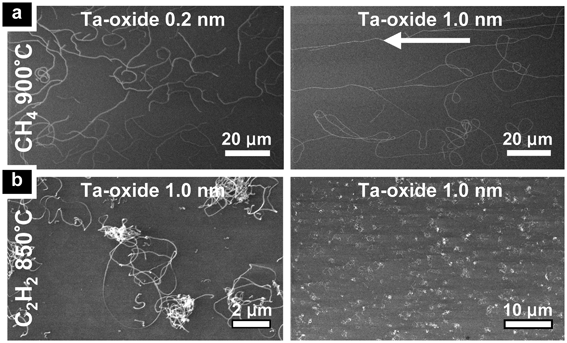 | ||
| Fig. 1 SEM images of typical growth results from (a) CH4-based and (b) C2H2-based CVD on SiO2 with varying CVD temperature and Ta-oxide thickness, as indicated in the figure. The arrow indicates process gas flow direction. Growth results are homogeneous across macroscopic samples. | ||
For CH4-based CVD the highest CNT yield is obtained on SiO2 support, for which the yield of randomly oriented tubes (∼40 μm length) at 900 °C and 0.1–0.2 nm Ta-oxide thickness is comparable to using a standard Fe catalyst53 (Fig. 1(a), left). An increase in Ta-oxide film thickness to 0.7–1.0 nm lowers the CNT yield but gives significantly longer and flow aligned tubes mixed with some short, unaligned tubes (Fig. 1(a), right). The flow aligned CNTs exceed 400 μm in length. AFM and TEM analysis (Fig. 2(a,b,c)) shows that the CH4 grown CNTs are single-walled with diameters of 0.6 nm to 3 nm. For CVD temperatures below 900 °C or catalyst film thicknesses in excess of 1 nm no CNT growth is observed for CH4-based CVD.
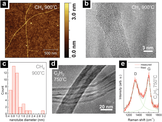 | ||
| Fig. 2 (a) Typical AFM scan of CH4 grown nanotubes (900 °C with 0.2 nm thick Ta-oxide on SiO2). (b) TEM image of a CH4 grown SWNT (900 °C with 0.2 nm Ta-oxide grown on SiO2 TEM membrane). Note that the SWNT is coated with amorphous carbon from TEM characterisation. (c) Histogram of AFM- and TEM-extracted diameters for CH4 grown nanotubes from 0.2 nm thick Ta-oxide on SiO2. The observed diameter range clearly indicates SWNT formation. (d) TEM image of C2H2 grown nanotubes (750 °C with 0.5 nm Ta-oxide on SiO2, scratched off onto the TEM grid). The diameter range and the hollow cores indicate MWNT formation. (e) Raman spectrum (633 nm) of C2H2 grown nanotubes (750 °C with 0.7 nm Ta-oxide on SiO2). The G and D features in the Raman spectrum are consistent with MWNT formation.34 Fitting the G and D Raman features with Lorentzians, a D/G ratio of ∼0.9 is obtained, comparable to D/G ratios for standard Fe catalysts under the same C2H2 750 °C CVD conditions.34 | ||
Changing to Al2O3 support results in a higher onset temperature for CNT growth of 950 °C, at which short (∼5 μm) and sparse CNTs are found for Ta-oxide film thicknesses ranging from 0.2 to 1.0 nm (see Supplementary Fig. 1 in the ESI). Native oxide covered Si wafers as support show no CNT growth for any of the conditions tested.
For C2H2-based CVD at comparatively lower temperatures (650 °C–750 °C) entangled bundles of short, curled tubes are observed for SiO2 supported Ta-oxide films with thicknesses ranging from 0.2 to 0.7 nm. At a growth temperature of 850 °C the CNTs nucleate from 0.2 to 2.0 nm thick Ta-oxide films, with an optimum yield for 1.0 nm thick Ta-oxide (Fig. 1(b)). For Ta-oxide films thicker than 2 nm no CNTs are observed. This appears consistent with recent literature, which reports no observable CNT growth from ambient air exposed 3 nm Ta films under similar CVD conditions.46Fig. 2(d) shows that Ta-oxide catalysed nanotubes are multi-walled for the C2H2-based CVD recipes with diameters of 10–25 nm. The multi-walled nature of the nanotubes is corroborated by the Raman analysis in Fig. 2(e).34 For typical 750 °C grown tubes we find in Fig. 2(e) a D/G intensity ratio of ∼0.9 which is the same as for Fe catalyst reference samples grown under the same CVD conditions.34 This confirms that the Ta-oxide films on SiO2 facilitate growth of nanotubes of reasonable quality.
The same Ta-oxide films on Al2O3 support with C2H2 show a higher growth onset temperature of ∼850 °C, at which only sparse, uncontrolled growth of entangled CNT bundles is observed for 0.7 to 1.0 nm Ta. Consistent with the CH4 results, for Si wafers covered only with a native oxide as support no CNT growth is observed for any of the conditions sampled for C2H2.
In order to rationalise this growth behaviour, we systematically analyse the state of the Ta in the catalyst films during the CVD process by in situ XPS. Fig. 3 compares the changes in Ta4f core level signatures upon vacuum annealing of 0.2 nm Ta-oxide supported on SiO2 (200 nm SiO2 on Si-wafer) and native oxide covered Si (∼2 nm SiO2). In the text we refer the binding energies of the various Ta chemical states to the Ta4f7/2 peak which is labelled with the respective state assignments in all XPS figures. The second peak feature at higher binding energy (with a constant offset of ∼1.9 eV to the Ta4f7/2) is the corresponding Ta4f5/2 for the same chemical state.
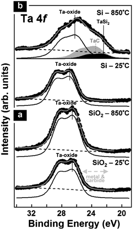 | ||
| Fig. 3 In situ XPS of 0.2 nm Ta-oxide films on (a) SiO2 and (b) Si at room temperature (as deposited) and during annealing at 850 °C in ∼10−8 mbar vacuum (5 min). While on SiO2 the Ta-oxide remains oxidised during annealing, on Si partial Ta-silicidation occurs. (We additionally observe Ta-carbide formation on Si, which we ascribe to interaction with adventitious carbon from transport in air.) | ||
In their as-deposited state (after air exposure), the films show only peaks corresponding to Ta-oxides (Ta4f7/2 at 26.2 ± 0.2 eV).43,52,55–57 As expected for very thin Ta films after ambient air exposure,33,52 oxidation of the entire films is confirmed and no peaks corresponding to Ta-metal (Ta4f7/2 ∼22 eV) or Ta-carbide (Ta4f7/2 ∼23.3 eV) are found.43,52,55–57
When heated in vacuum, the thin Ta-oxide on SiO2 support does not change its chemical state, i.e., it stays oxidised even at 850 °C (Fig. 3(a)). This is in dramatic contrast to the behaviour seen for surface Ta-oxide on thicker Ta films (∼100 nm on SiO2), where we found that the surface oxide readily reduces under similar annealing conditions.34 This suggests that the thin Ta-oxide is interfacially stabilised by the close proximity to the SiO2 support.
On the contrary, Fig. 3(b) shows that on the ∼2 nm native oxide support a partial silicidation, i.e. formation of TaSi2, occurs during the high temperature annealing (Ta4f7/2 at ∼22.6 eV).58–60 Additionally we observe Ta-carbide formation (Ta4f7/2 ∼23.5 eV), most likely due to the interaction with adventitious carbon from the sample transfer in air and facilitated by the silicidation reaction. This silicon-mediated Ta-oxide reduction and Ta-silicidation clearly explains why no CNT growth is observed for the native oxide support. The approximately 2 nm thick native oxide is not sufficiently thick to isolate the Ta atoms from the bulk Si. The resulting silicide formation leads to deactivation of the catalyst similar as in the case of standard catalysts.61 It is however important to note that the as-formed Ta silicide gets re-oxidised upon air exposure over the duration of several days. This can obscure the actual differences between the thick SiO2 and native oxide support for ex-situ XPS and hence this clearly highlights the motivation for our in situ measurements.
Fig. 4 shows process-step resolved Ta4f core level signatures recorded by synchrotron-based in situ XPS during low pressure H2 and C2H2 exposures (0.5 mbar) of a SiO2 (200 nm) supported 0.5 nm thick Ta-oxide film at ∼750 °C.
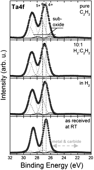 | ||
| Fig. 4 Process-step resolved in situ XPS of a 0.5 nm Ta-oxide film on SiO2 during low pressure CVD at ∼750 °C in a total pressure of ∼0.5 mbar. From bottom to top: As loaded catalyst film at room temperature, at 750 °C in 0.5 mbar H2, at 750 °C in 0.5 mbar H2/C2H2 (10:1) and at 750 °C in 0.5 mbar C2H2. Notably, the Ta remains in an oxidised state during the process (Ta4+ and Ta5+), never showing carbidic or metallic components. | ||
Compared to the lab-source-based XPS scans in Fig. 3 and Fig. 5, the synchrotron-based XPS has a higher resolution, allowing us to resolve the contributions of particular oxidation states in the Ta-oxide. In Fig. 4, the XPS signature of the as-loaded Ta film is dominated by contributions of Ta4+ (Ta4f7/2 ∼26.7 eV) and Ta5+ (Ta4f7/2 ∼27.2 eV) oxidation states. This signature does not significantly change during annealing in ∼0.5 mbar H2, neither for the subsequent addition of C2H2, nor for the final CVD atmosphere of ∼0.5 mbar of undiluted C2H2. Again we find that these SiO2 supported thin Ta-oxide films are much less reactive than surface Ta-oxides on thicker metallic Ta films (∼100 nm Ta on SiO2) that were readily transformed to a carbide under such C2H2 exposure conditions.34 This again suggests interfacial stabilisation of the thin Ta-oxide by the SiO2 support where the Ta-oxide is preserved even in strongly reducing environments.
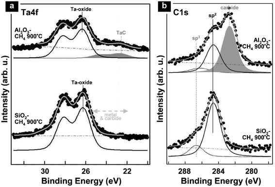 | ||
| Fig. 5 Ex-situ (a) Ta4f and (b) C1s XPS scans of 0.2 nm Ta-oxide films after CH4-based CVD at 900 °C on (from bottom to top) SiO2 (CNT growth) and Al2O3 (no growth). On SiO2, the Ta4f spectrum shows only signals corresponding to Ta-oxide. On Al2O3, the dominant feature is also Ta-oxide but a Ta-carbide contribution is additionally found (matched by a corresponding carbide signature in (b)). | ||
We note that due to the pressure limitations of the in situ XPS set-up54 the Ta phase during the atmospheric CNT CVD conditions cannot be directly probed. We hence carried out a range of complementary ex-situ XPS measurements. Fig. 5 shows such ex-situ XPS scans after atmospheric CH4-based CVD at 900 °C for 0.2 nm thick Ta-oxide supported on SiO2 and Al2O3. Consistent with the in situ XPS, the post-growth signature of SiO2 supported thin Ta-oxide only shows peaks corresponding to Ta-oxides (Ta4f7/2 at ∼26.2 eV), while no peaks corresponding to Ta-metal (Ta4f7/2 ∼22 eV) and -carbide (Ta4f7/2 ∼23.3 eV) are found.43,52,55–57 The post growth C1s signature shows sp2-bound carbon (C1s ∼284.5 eV), in agreement with the SEM observations of grown nanotubes (Fig. 1(a), left). Interestingly, the Al2O3 supported Ta-oxide films show additional peaks at 23.1 ± 0.2 eV in the Ta4f energy region and at 282.7 ± 0.2 eV in the C1s energy region after CVD processing with CH4 at 900 °C (Fig. 5). The additional peaks can be attributed to Ta-carbide (where the ∼284.5 eV signal in the C1s region is attributed to graphitic fragments as no nanotube were grown at 900 °C on Al2O3).43,52,55–57 The admixture of Al/Al2O3 to Ta-oxides is known to change the oxides' structural evolution with temperature62,63 and may lower the temperature for partial Ta-oxide reduction.64 This could relate to the observed carbide formation here. This carbide formation may in turn relate to the lower CNT growth yield and higher growth onset temperatures we observed for Al2O3 supported Ta-oxide films.
4. Discussion
In a previous study regarding Ta-containing bimetallic FeTa co-catalysts for CNT growth,47 we exposed similarly thin, ambient air exposed Ta films to low pressure CVD but did not find CNT growth. This is in contrast to the successful atmospheric pressure CNT CVD presented here, which suggests that Ta-based catalysts need a high partial pressure of the carbon source, similar to most non-standard catalysts. Furthermore, the growth data in the present study also highlights the importance of a low initial Ta-oxide film thickness for CNT nucleation.Previous reduction studies on Ta-oxides found that Ta-oxide reduction by H264,65 as well as carbothermal reduction66 require temperatures in excess of 1050 °C, significantly above our CVD conditions. In a previous study we have also established the presence of significant amounts of residual oxygen/water in our atmospheric CVD system even in nominally reducing gas mixtures.34 Considerations of the Ta–C–O phase diagram at 600–750 °C have suggested that Ta-oxide is stable over TaC when a small oxygen partial pressure is present.67 This leads us to hypothesise that, as with ZrO2,20 the Ta-based catalyst during nanotube growth is actually in its oxide form for our CVD conditions. This is in agreement with the key observation that for the thin Ta-oxide films on SiO2, the substrate that allowed SWNT and MWNT growth with the highest yield, all our in situ and ex-situ XPS measurements showed no carbidic or metallic Ta-components but only Ta-oxide.
Additionally, when phases other than Ta-oxides were detected by XPS in the films the CNT growth yield was greatly reduced. On the Si support we found that the formation of Ta-silicides hindered CNT growth completely and on the Al2O3 support we found that the presence of Ta-carbide (in addition to the oxide) correlates with a greatly reduced CNT growth window. Combination of these observations corroborates an interpretation of our data towards Ta being an active CNT catalyst in its oxide form under our CVD conditions.
5. Conclusions
We find that technologically important, ULSI-process compatible Ta-oxide thin films catalyse SWNT growth with CH4 and MWNT growth with C2H2 (at moderate temperatures as low as 650 °C). This is important as most non-standard catalysts only catalyse high temperature SWNT growth. A low film thickness, the nature of the support material (where best results were observed with SiO2), and atmospheric process gas pressure are of key importance for successful nanotube nucleation. Strong material interactions, such as silicide formation on Si, inhibit CNT growth. Our ex- and in situ characterisation data suggests that no catalyst reduction to Ta-metal or Ta-carbide occurs during our CVD conditions and that the catalytically active phase is the Ta-oxide phase.Acknowledgements
S.H. acknowledges funding from the EPSRC (Grant No. EP/H047565/1) and from ERC grant InsituNANO (project reference 279342). We acknowledge the Helmholtz-Zentrum-Berlin BESSY II synchrotron, and we thank the BESSY staff for continuous support. We acknowledge partial funding from the EC project Technotubes. C.D. acknowledges the Royal Society for funding and B.C.B. acknowledges a Research Fellowship from Hughes Hall, Cambridge.References
- S. Hofmann, R. Sharma, C. Ducati, G. Du, C. Mattevi, C. Cepek, M. Cantoro, S. Pisana, A. Parvez, F. Cervantes-Sodi, A. C. Ferrari, R. Dunin-Borkowski, S. Lizzit, L. Petaccia, A. Goldoni and J. Robertson, Nano Lett., 2007, 7, 602 CrossRef CAS.
- J.-P. Tessonnier and D. S. Su, ChemSusChem, 2011, 4, 824 CrossRef CAS.
- M. Fouquet, B. C. Bayer, S. Esconjauregui, R. Blume, J. H. Warner, S. Hofmann, R. Schlögl, C. Thomsen and J. Robertson, Phys. Rev. B: Condens. Matter Mater. Phys., 2012, 85, 235411 Search PubMed.
- C. T. Wirth, B. C. Bayer, A. D. Gamalski, S. Esconjauregui, R. S Weatherup, C. Ducati, C. Baehtz, J. Robertson and S. Hofmann, Chem. Mater., 2012, 24, 4633 Search PubMed.
- W. Zhou, Z. Han, J. Wang, Y. Zhang, J. Zhong, X. Sun, Y. Zhang, C. Yan and Y. Li, Nano Lett., 2006, 6, 2987 CrossRef CAS.
- D. Takagi, Y. Homma, H. Hibino, S. Suzuki and Y. Kobayashi, Nano Lett., 2006, 6, 2642 CrossRef CAS.
- D. Yuan, L. Ding, H. Chu, Y. Feng, T. P. McNicholas and J. Liu, Nano Lett., 2008, 8, 2576 CrossRef CAS.
- S. Bhaviripudi, E. Mile, S. A. Steiner III, A. T. Zare, M. S. Dresselhaus, A. M. Belcher and J. Kong, J. Am. Chem. Soc., 2007, 129, 1516 CrossRef CAS.
- S. Esconjauregui, C. M. Whelan and K. Maex, Carbon, 2009, 47, 659 CrossRef CAS.
- T. Uchino, K. N. Bourdakos, C. H. de Groot, P. Ashburn, M. E. Kiziroglou, G. D. Dilliway and D. C. Smith, Appl. Phys. Lett., 2005, 86, 233110 Search PubMed.
- D. Takagi, H. Hibino, S. Suzuki, Y. Kobayashi and Y. Homma, Nano Lett., 2007, 7, 2272 CrossRef CAS.
- D. Takagi, Y. Kobayashi and Y. Homma, J. Am. Chem. Soc., 2009, 131, 6922 CrossRef CAS.
- X. Yu, J. Zhang, W. Choi, J.-Y. Choi, J. M. Kim, L. Gan and Z. Liu, Nano Lett., 2010, 10, 3343 CrossRef CAS.
- J. H. Lin, C. S. Chen, M. H. Ruemmeli, A. Bachmatiuk, Z. Y. Zeng, H. L. Ma, B. Buechner and H. W. Chen, Chem. Mater., 2011, 23, 1637 CrossRef CAS.
- H. Liu, D. Takagi, H. Ohno, S. Chiashi, T. Chokan and Y. Homma, Appl. Phys. Express, 2008, 1, 014001 Search PubMed.
- E. J. Bae, W. B. Choi, K. S. Jeong, J. U. Chu, G.-S. Park, S. Song and I. K. Yoo, Adv. Mater., 2002, 14, 277 CrossRef CAS.
- J. J. Schneider, N. I. Maksimova, J. Engstler, R. Joshi, R. Schierholz and R. Feile, Inorg. Chim. Acta, 2008, 361, 1770 CrossRef CAS.
- B. Liu, W. Ren, L. Gao, S. Li, S. Pei, C. Liu, C. Jiang and H. Cheng, J. Am. Chem. Soc., 2009, 131, 2082 CrossRef CAS.
- S. Huang, Q. Cai, J. Chen, Y. Qian and L. Zhang, J. Am. Chem. Soc., 2009, 131, 2094 CrossRef CAS.
- S. A. Steiner III, T. F. Baumann, B. C. Bayer, R. Blume, M. A. Worsley, W. J. MoberlyChan, E. L. Shaw, R. Schlögl, A. J. Hart, S. Hofmann and B. L. Wardle, J. Am. Chem. Soc., 2009, 131, 12144 CrossRef CAS.
- B. Liu, D.-M. Tang, C. Sun, C. Liu, W. Ren, F. Li, W.-J. Yu, L.-C. Yin, L. Zhang, C. Jiang and H.-M. Cheng, J. Am. Chem. Soc., 2011, 133, 197 CrossRef CAS.
- H. Liu, D. Takagi, S. Chiashi and Y. Homma, Carbon, 2010, 48, 114 CrossRef CAS.
- A. Bachmatiuk, F. Boerrnert, M. Grobosch, F. Schaeffel, U. Wolff, A. Scott, M. Zaka, J. H. Warner, R. Klingeler, M. Knupfer, B. Buechner and M. H. Ruemmeli, ACS Nano, 2009, 3, 4098 CrossRef CAS.
- A. J. Page, K. R. S. Chandrakumar, S. Irle and K. Morokuma, J. Am. Chem. Soc., 2011, 133, 621 CrossRef CAS.
- F. Gao, L. Zhang and S. Huang, Appl. Surf. Sci., 2010, 256, 2323 Search PubMed.
- Q. Cai, Y. Hu, Y. Liu and S. Huang, Appl. Surf. Sci., 2012, 258, 8019 Search PubMed.
- M. H. Rummeli, A. Bachmatiuk, A. Scott, F. Borrnert, J. H. Warner, V. Hoffman, J.-H. Lin, G. Cuniberti and B. Buchner, ACS Nano, 2010, 4, 4206 CrossRef.
- P. R. Kidambi, B. C. Bayer, R. S. Weatherup, R. Ochs, C. Ducati, D. V. Szabó and S. Hofmann, Phys. Status Solidi RRL, 2011, 5, 341 Search PubMed.
- J. Robertson, J. Mater. Chem., 2012, 22, 19858 RSC.
- C. P. Deck and K. Vecchio, Carbon, 2006, 44, 267 CrossRef CAS.
- Y. Homma, H. Liu, D. Takagi and Y. Kobayashi, Nano Res., 2009, 2, 793 CrossRef CAS.
- Binary Alloy Phase Diagrams, ed. T. B. Massalski, ASM International, USA, 2nd edn, 1990 Search PubMed.
- S. M. Cardonne, P. Kumar, C. A. Michaluk and H. D. Schwartz, Int. J. Refract. Met. Hard Mater., 1995, 13, 187 Search PubMed.
- B. C. Bayer, S. Hofmann, C. Castellarin-Cudia, R. Blume, C. Baehtz, S. Esconjauregui, C. T. Wirth, R. A. Oliver, C. Ducati, A. Knop-Gericke, R. Schlögl, A. Goldoni, C. Cepek and J. Robertson, J. Phys. Chem. C, 2011, 115, 4359 Search PubMed.
- S. M. Irving and P. L. Walker, Carbon, 1967, 5, 399 Search PubMed.
- S. A. Steiner III, Master's Thesis, Massachusetts Institute of Technology, 2006 Search PubMed.
- M. Terrones, W. K. Hsu, H. Terrones, J. P. Zhang, S. Ramos, J. P. Hare, R. Castillo, K. Prassides, A. K. Cheetham, H. W. Kroto and D. R. M. Walton, Chem. Phys. Lett., 1996, 259, 568 CrossRef CAS.
- H. Li, C. Xue, H. Zhuang, J. Chen, Z. Yang, L. Qin, Y. Huang and D. Zhang, Mater. Chem. Phys., 2008, 109, 249 Search PubMed.
- P. Nguyen, H. T. Ng and M. Meyyappan, Adv. Mater., 2005, 17, 1773 CrossRef CAS.
- T. Tanaka, H. Nojima, T. Yamamoto, S. Takenaka, T. Funabik and S. Yoshida, Phys. Chem. Chem. Phys., 1999, 1, 5235 RSC.
- T. Usjikubo, Catal. Today, 2000, 57, 331 CrossRef CAS.
- Y. Chen, J. L. G. Fierro, T. Tanaka and I. E. Wachs, J. Phys. Chem. B, 2003, 107, 5243 CrossRef CAS.
- J. Choi, Appl. Catal., A, 1999, 184, 189 Search PubMed.
- I. Kojima, E. Miyazaki, Y. Inoue and I. Yasumori, J. Catal., 1982, 73, 128 CrossRef CAS.
- J.-G. Choi, H.-G. Oh and Y.-S. Baek, J. Ind. Eng. Chem., 1998, 4, 94 Search PubMed.
- G. D. Nessim, M. Seita, K. P. O'Brien and S. A. Speakman, Carbon, 2010, 48, 4519 Search PubMed.
- B. C. Bayer, M. Fouquet, R. Blume, C. T. Wirth, R. S. Weatherup, K. Ogata, A. Knop-Gericke, R. Schlögl, S. Hofmann and J. Robertson, J. Phys. Chem. C, 2012, 116, 1107 Search PubMed.
- CRC Handbook of Chemistry and Physics, ed. R. C. Weast, CRC press, Cleveland, Ohio, USA, 56th edn, 1975 Search PubMed.
- R. Steinitz and R. Resnick, J. Appl. Phys., 1966, 37, 3463 Search PubMed.
- C. Chaneliere, J. L. Autran, R. A. B. Devine and B. Balland, Mater. Sci. Eng., R, 1998, 22, 269 CrossRef.
- H. Qian, E. S. Greenhalgh, M. S. P. Shaffer and A. Bismarck, J. Mater. Chem., 2010, 20, 4729 RSC.
- M. Khanuja, H. Sharma, B. R. Mehta and S. M. Shivaprasad, J. Electron Spectrosc. Relat. Phenom., 2009, 169, 41 Search PubMed.
- S. Pisana, A. Jungen, C. Zhang, A. M. Blackburn, R. Sharma, F. Cervantes-Sodi, C. Stampfer, C. Ducati, A. C. Ferrari, C. Hierold, J. Robertson and S. Hofmann, J. Phys. Chem. C, 2007, 111, 17249 Search PubMed.
- A. Knop-Gericke, E. Kleimenov, M. Hävecker, R. Blume, D. Teschner, S. Zafeiratos, R. Schlögl, V. I. Bukhtiyarov, V. V. Kaichev, I. P. Prosvirin, A. I. Nizovskii, H. Bluhm, A. Barinov, P. Dudin and M. Kiskinova, Adv. Catal., 2009, 52, 213 CAS.
- D. Yang, H. Jiang, R. Ott, K. Minor, J. Grant, L. Varga, J. A. Barnard and W. D. Doyle, Surf. Interface Anal., 1999, 27, 259 Search PubMed.
- E. Atanassova, G. Tyuliev, A. Paskaleva, D. Spassov and K. Kostov, Appl. Surf. Sci., 2004, 225, 86 CrossRef CAS.
- B. S. Itchkawitz, P. F. Lyman, G. W. Ownby and D. M. Zehner, Surf. Sci., 1994, 318, 395 Search PubMed.
- A. Y. Mao, K. A. Son, J. M. White, D. L. Kwong, D. A. Roberts and R. N. Vrtis, J. Vac. Sci. Technol., A, 1999, 17, 954 Search PubMed.
- S. Kohli, P. R. McCurdy, C. D. Rithner, P. K. Dorhout, A. M. Dummer, F. Brizuela and C. S. Menoni, Thin Solid Films, 2004, 469-470, 404 Search PubMed.
- X. Zhao, N. P. Magtoto, M. Leavy and J. A. Kelber, Thin Solid Films, 2002, 415, 308 Search PubMed.
- J. M. Simmons, B. M. Nichols, M. S. Marcus, O. M. Castellini, R. J. Hamers and M. A. Eriksson, Small, 2006, 2, 902 Search PubMed.
- S. Wu, H. M. Chan and M. P. Harmer, J. Am. Ceram. Soc., 2005, 88, 2369 Search PubMed.
- M. K. Hota, C. Mahata, M. K. Bera, S. Mallik, C. K. Sarkar, S. Varma and C. K. Maiti, Thin Solid Films, 2010, 519, 423 Search PubMed.
- J. P. Kim, Korean J. Chem. Eng., 2004, 21, 385 Search PubMed.
- I. E. Wachs, Y. Chen, J. Jehng, L. E. Briand and T. Tanaka, Catal. Today, 2003, 78, 13 CrossRef CAS.
- D. Kwon, S. Hong and B. Kim, Mater. Lett., 2004, 58, 3863 Search PubMed.
- T. Laurila, K. Zeng, J. K. Kivilahti, J. Molarius and I. Suni, Appl. Phys. Lett., 2002, 80, 938 Search PubMed.
Footnote |
| † Electronic supplementary information (ESI) available. See DOI: 10.1039/c3ra23304a |
| This journal is © The Royal Society of Chemistry 2013 |