First-principles study on the doping effects of nitrogen on the electronic structure and optical properties of Cu2O
Zongyan
Zhao
*a,
Xijia
He
b,
Juan
Yi
b,
Chenshuo
Ma
b,
Yuechan
Cao
b and
Jianbei
Qiu
c
aKunming University of Science and Technology – School of Materials Science and Engineering, 293 Xuefu Road, Kunming, Yunnan 650093, China. E-mail: zzy@kmust.edu.cn; Fax: +86-871-518-8856; Tel: +86-871-518-8856
bKunming University of Science and Technology – School of Materials Science and Engineering, Kunming, Yunnan, China
cKuming University of Science and Technology – College of Materials Science and Engineering, Xuefu Road 253, Kunming, 650093, China
First published on 25th October 2012
Abstract
Recent experimental literature (Sol. Energ. Mat. Sol. Cells, 2012, 105, 192) has reported that nitrogen doped Cu2O is a possible material for novel intermediate band solar cells. The doping effects of nitrogen on the crystal structure, electronic structure, and optical properties of Cu2O have been studied by an ultrasoft pseudopotential plane wave method based on first-principles calculations. The results show that nitrogen doping slightly widens the band gap of Cu2O, and form an intermediate band in the gap located at about 0.9 eV from the VBM (or CBM). This intermediate band is predominantly formed by hybridization between the N-2p states and the Cu-3d states. N-doped Cu2O is very likely to absorb at a maximum across the solar light spectrum, from the near infrared region to the ultraviolet region. Based on these results, N-doped Cu2O is considered to be a perfect intermediate band material for a novel kind of solar cells.
1. Introduction
As an important functional optoelectronic semiconductor, cuprous oxide (Cu2O) has shown great potential for applications in electronics, gas sensors, communication, energy, environmental protection, and so on, due to its unique electronic and optical properties.1–3 Further advantages are nontoxicity, low-cost production processing and the fact that its component elements are very abundant in the Earth’s crust. In addition, it possesses a direct gap of 1.9–2.1 eV,4,5 and has a considerable absorption coefficient, up to ∼104 cm−1, in the visible-light region of the solar light spectrum. Therefore, it is especially suitable for applications in photovoltaics and photocatalysis, and has attracted extensive concern in these fields over the past few decades.6–11In the field of photovoltaics, copper and copper oxide (metal-semiconductor) is one of the first photovoltaic cells, invented by Pollack and Trivich in 1975.12 Since then, Cu2O-based thin film solar cells were fabricated by various experimental approaches, including direct thermal oxidation,11,13 RF magnetron sputtering,14 solvent-thermal processes,15 electrochemical deposition,16–20etc. The corresponding photovoltaic properties have been investigated in detail. For example, Cu2O-based thin film solar cells exhibit high conversion efficiencies for solar light in the range from about 550 nm to near ultraviolet, where the conversion efficiency of crystalline silicon solar cells begins to decrease significantly.6 Although Cu2O has numerous advantages, as mentioned above, the energy conversion efficiency of Cu2O-based thin film solar cells has improved very slowly over the last few decades. Up to now, the best energy conversion efficiency of Cu2O-based thin film solar cells is 3.83%, reported by Minami et al.6 In fact, the theoretical limit of the energy conversion efficiency for a Cu2O-based thin film solar cell is as high as about 20%, according to Shockley–Queisser photo balance calculations.21 Experimental efficiency is quite low compared with the theoretical limit, and thus more systematic study is needed for this material.
Based on previous research, it is found there are two major reasons leading to such low energy conversion efficiency of Cu2O-based thin film solar cells. Firstly, Cu2O is a spontaneous p-type semiconductor, owing to the presence of large number of copper vacancies that act as a shallow and efficient hole producer.22 The self compensation effects make it difficult to acquire n-type Cu2O, so the preparation of the p–n homojunction is particularly difficult. Secondly, its band gap is about 1.9–2.1 eV. Although it can absorb most of the energy in the solar spectrum, it still larger than the optimum band gap (∼1.5 eV) of solar cells,21 resulting in it being unable to achieve the maximum energy conversion efficiency. To address the former drawback, researchers have recently attempted different ion doping to obtain n-type Cu2O thin films.17,23 But these thin films have low carrier concentration and mobility, leading to high total resistivity. Thus, the energy conversion efficiency of the prepared p–n homojunction solar cells is very low, only about 0.1%.17 Therefore, some researchers have transferred their focus to the latter, namely attempting to develop Cu2O-based third generation solar cells based on the intermediate band (IB) absorption processes, due to its band gap making it a perfect candidate for this kind of novel solar cell.24 Recently, Malerba et al. first reported that nitrogen doped Cu2O could act as a possible material for IB solar cells.25 They found that all the N-doped samples exhibit two clearly defined absorption bands at energies below the band gap. In the earlier published literature, researchers found that nitrogen can be easily incorporated into the crystal lattice of Cu2O at high concentration to substitute oxygen atoms and act as a p-type dopant.26,27
On the one hand, we considered that it is very necessary to understand more deeply the nature of nitrogen doping for Cu2O, motivated by these novel results. On the other hand, we found that there is some controversy in the published literature. For example, Nakano et al. reported a widening in the band gap of N-doped Cu2O thin films.27 But other researchers observed that Cu2O with nitrogen impurities did not show any band gap change.25,26 Furthermore, the position of impurity energy levels, i.e. IB, of nitrogen is still not clearly defined. In order to solve these problems, we systematically studied the doping effects of nitrogen on the electronic structure and optical properties of Cu2O in this work, using first-principles calculations.
2. Computational model and method
The supercell model of N-doped Cu2O considered in the present work is shown in Fig. 1. Cu2O has a high symmetry cubic structure (point group: O4h; space group: 224, Pn![[3 with combining macron]](https://www.rsc.org/images/entities/char_0033_0304.gif) m). It has six atoms per unit cell: the oxygen atoms form a bcc lattice, while the copper are on the vertices of a tetrahedron around each oxygen atom. In the case of the nitrogen doping model, a 2 × 2 × 2 supercell was adopted as shown in Fig. 1, in which one oxygen atom was substituted by one nitrogen atom. Thus, the nitrogen concentration is about 2.08% (atomic fraction, equal to 1.6 × 1021 cm−3) in total, which was comparable to that used in the experiments.25
m). It has six atoms per unit cell: the oxygen atoms form a bcc lattice, while the copper are on the vertices of a tetrahedron around each oxygen atom. In the case of the nitrogen doping model, a 2 × 2 × 2 supercell was adopted as shown in Fig. 1, in which one oxygen atom was substituted by one nitrogen atom. Thus, the nitrogen concentration is about 2.08% (atomic fraction, equal to 1.6 × 1021 cm−3) in total, which was comparable to that used in the experiments.25
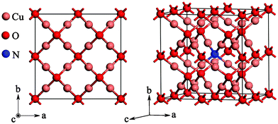 | ||
| Fig. 1 The supercell model of N-doped Cu2O considered in the present work. | ||
In the present work, all of the calculations were carried out using the periodic density functional theory package of Cambridge Serial Total Energy Package (CASTEP) codes.28 CASTEP is a state-of-the-art quantum mechanics-based program designed specifically for solid-state materials science. The core electrons (Cu: [Ar], O and N: [He]) were treated with the ultrasoft pseudopotential. The exchange–correlation effects of valence electrons (Cu: 3d104s1, O: 2s22p4, N: 2s22p3) were described through the generalized gradient approximation (GGA), within the Perdew–Burke–Ernzerhof (PBE) function.29 In order to obtain an accurate electronic structure, the method of GGA + U was adopted to overcome the well-known shortcoming of GGA (Ueff = U − J = 8.5 eV).30 The Hubbard model is one of the most successful models used to describe the correlated electrons in solids. To construct an appropriate function the GGA + U approach subdivides charge density into two subsystems: delocalized and localized. The former remains described by its charge density, while for the latter a site diagonal charge density matrix is introduced. The Monkhorst–Pack scheme k-points grid sampling was set as 4 × 4 × 4 for the irreducible Brillouin zone. A 30 × 30 × 30 mesh was used for fast Fourier transformation. An energy cutoff of 440 eV was used for expanding the Kohn–Sham wave functions. The minimization algorithm was chosen to be the Broyden–Fletcher–Goldfarb–Shanno (BFGS) scheme.31 Its convergence criteria were set as follows: the force on the atoms was less than 0.01 eV Å−1, the stress on the atoms was less than 0.02 GPa, the atomic displacement was less than 5 × 10⁻⁴ Å, and the energy change per atom was less than 5 × 10⁻⁶ eV. Based on the optimized crystal structure, the electronic structure and the optical properties were then calculated.
3. Results and discussions
By optimizing the pure Cu2O crystal structure, we obtained the lattice parameters as follows: a = b = c = 4.2376 Å. They were in good agreement with experimental values: a = b = c = 4.2696 Å.32 These results implied that our calculation methods are reasonable, and the calculated results should be authentic. The lattice parameters of pure and N-doped Cu2O are displayed in Table 1. Furthermore, we found that the configuration between Cu atoms and O atoms is linear, namely the bond angle of O–Cu–O is equal to 180°. This feature did not change in the nitrogen doping model (the bond angles of O–Cu–N and O–Cu–O are still equal to 180°). When point defects are introduced into the host lattice, lattice distortion usually occurs, owing to the differences in ion radius and valence electron configuration. But in the present work, we found that the lattice distortions are not obvious for the nitrogen doping model. Therefore, even with the introduction of nitrogen impurities, Cu2O still maintains its original exceptional photoelectric performance. Next, we analyzed the impurity formation energy for the nitrogen doping model. This is a widely accepted approach to compare the relative degree of difficulty for incorporation of an impurity into the host lattice. In the present work, the formula of impurity formation energy is referred to using the formalism defined by Van de Walle and Neugebauer.33 The calculated results are also listed in Table 1. These results imply that nitrogen impurities could be readily incorporated into the crystal lattice of Cu2O under O-poor conditions, i.e. a reducing atmosphere.| Lattice parameters/Å | Impurity formation energy/eV | Band gap/eV | ||
|---|---|---|---|---|
| O rich | O poor | |||
| Pure Cu2O | 4.2376 | 2.085 | ||
| N-doped Cu2O | 4.2345 | 2.65 | −2.70 | 2.101 |
The calculated band structure and density of states (DOS) of pure and N-doped Cu2O are plotted and compared in Fig. 2 and Fig. 3. As shown in Fig. 2, we found that pure Cu2O is an indirect band gap semiconductor and that the valence band maximum (VBM) and the conduction band minimum (CBM) are located at the same k-point, Γ. And the calculated band gap of pure Cu2O is 2.085 eV between VBM and CBM, which is very close to the experimental observations.25,27 For pure Cu2O, the number of up-spin electrons is equal to the number of down-spin electrons. Thus, we did not find the spin-polarization phenomenon in the figure of band structure and density of states. The upper valence band (VB) is dominated by the Cu-3d states, while the VB located in the region −10 ∼ −6 eV mainly consists of O-2p states. The lower conduction band (CB) does not exhibit the electronic states of single atoms, but more exhibits the hybridized states between them. In the case of nitrogen doping, the band gap is slightly widened from 2.085 to 2.101 eV. This calculation result is consistent with some reported experimental observations.27 But the change in band gap is very small, so it might not be observed in other experiments.25 In addition, there is a spin-polarization above the top of the VB, in which spin-down impurity energy levels, i.e. IB, are located in the range 0.903 to 0.1.176 eV, with a band width of 0.273 eV. The impurity energy levels are mainly contributed to from the N-2p states, but other electronic states, O-2p and Cu-3p, -3d, -4s, also contribute to the formation of the IB. Using this IB, the electrons on the top of the VB could transfer not only from the VB to the CB (VB → CB), but also firstly from the VB to the IB and subsequently to the CB (VB → IB → CB), resulting in absorption of a lower energy photon. The position of the IB, about 0.9 eV from the VBM (or CBM), meets very well the requirement of a high energy conversion efficiency of intermediate band solar cells.24 Therefore, we may answer the question proposed by Malerba et al. N-doped Cu2O is a perfect IB material for the novel kind of solar cells, owing to its suitable band gap and suitable position of the IB.
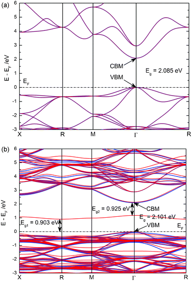 | ||
| Fig. 2 The calculated band structure along the high symmetry directions of the Brillouin zone of pure (a) and N-doped (b) Cu2O. The blue lines represent the spin-up states, while the red lines represent spin-down states. | ||
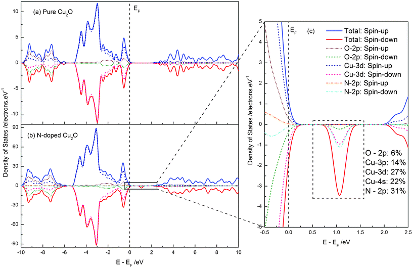 | ||
| Fig. 3 The total and local partial density of states of pure (a) and N-doped (b) Cu2O. (c) The enlarged view of electronic states near the band gap of N-doped Cu2O, and the component of IB is also given. . | ||
To further examine the chemical bonding features, the projected contour maps of the electronic wave function at the VBM, CBM, and IB are plotted in Fig. 4. At the VBM, for pure Cu2O (as shown in Fig. 4(a)), O-2p states occupy the entire space, and exhibit interplay with the neighboring Cu-3d states. So it has the π bonding state characteristics that arise from hybridization of Cu-3dx2−y2 (or -3dz2) states and O-2pπ states. While for the N-doped Cu2O (as shown in Fig. 4(c)), the most predominant states are the N-2p states. So the characteristic π bonding states between O atoms and Cu atoms are not obvious, compared to the case of pure Cu2O. In particularly, the hybridization between the N atom and its two neighboring Cu atoms is stronger than that these two V atoms with their neighboring O atoms. At CBM, for pure Cu2O (as shown in Fig. 4(b)), the bonding features mainly exhibit the π anti-bonding states between Cu-3dx2−y2 (or -3dz2) states and O-2pπ states. But in the case of N-doped Cu2O (as shown in Fig. 4(d)), this feature around the N atom is weaker than that around O atoms. For the impurity energy levels, i.e. IB (as shown in Fig. 4(e)), the most predominant states are the hybridization between N-2p states and Cu-3d states.
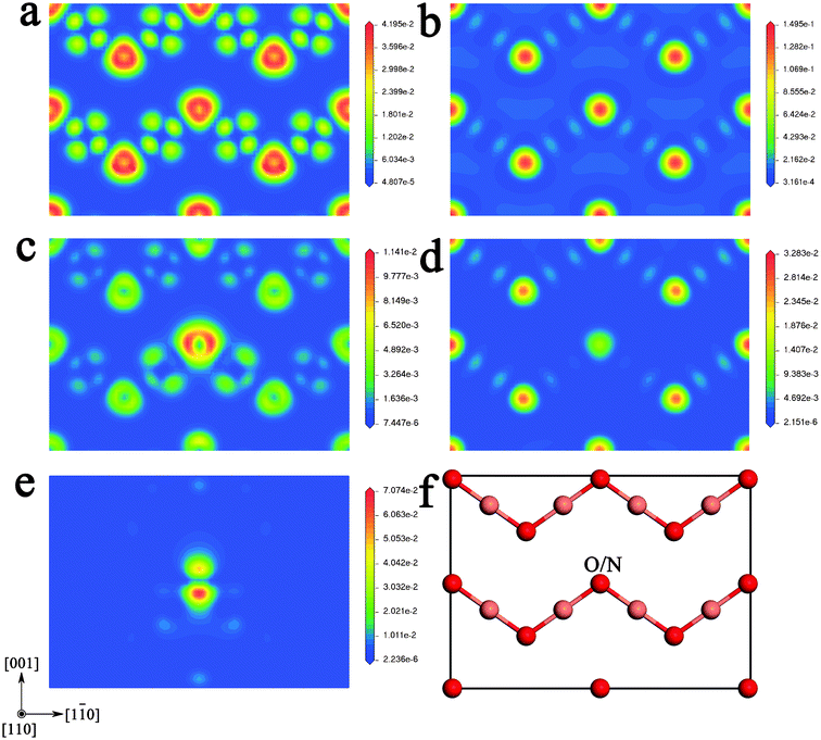 | ||
| Fig. 4 The projected wave function contour plots through the (110) plane of pure and N-doped Cu2O at different energy levels. (a) At the VBM of pure Cu2O; (b) at the CBM of pure Cu2O; (c) at the VBM of N-doped Cu2O; (d) at the CBM of N-doped Cu2O; (e) at the IB of N-doped Cu2O; and (f) the atomic positions on the (110) plane. | ||
In order to deepen our understanding of the doping effects of nitrogen on the electronic structure of Cu2O, we further analyzed and compared the electron density difference of pure and N-doped Cu2O, as showed in Fig. 5. Firstly, the electron density difference of N-doped Cu2O is very similar to pure Cu2O on lattice positions far away from the nitrogen impurity. This result indicates that the effect of nitrogen point defects is a local effect that only impacts the local electronic structure. Secondly, in the case of N-doped Cu2O, the electron density around the nitrogen impurity evidently increases on the (110) plane. These results indicate that the magnitude of electron transfer from metal atoms to non-metal atoms in these two models is different. Owing to the larger electronegativity, the nitrogen atom could attract more electrons. To quantitatively exhibit this doping effect, we listed the results of Mulliken population analysis in Table 2. The population on the O atoms and Cu atoms did not change after nitrogen doping. But the populations on the Cu–O bonds increase in the N-doped Cu2O. And the populations on the N atom and Cu–N bonds are obviously larger than those on the O atoms and Cu–O bonds, respectively.
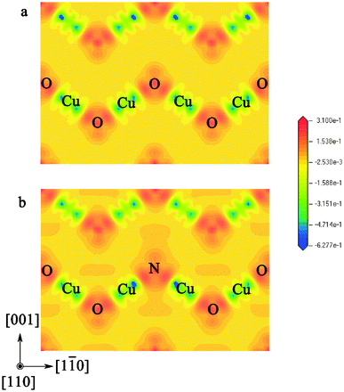 | ||
| Fig. 5 The calculated electron density difference of pure (a) and N-doped (b) Cu2O. The atomic positions are the same as in Fig. 4(f). | ||
| Species | s | p | d | Total | Charge/e | Bond | Length/Å | Population/e | |
|---|---|---|---|---|---|---|---|---|---|
| Pure Cu2O | O | 1.81 | 4.83 | 6.64 | −0.64 | Cu–O | 1.8350 | 0.33 | |
| Cu | 0.58 | 0.48 | 9.62 | 10.68 | 0.32 | ||||
| N-doped Cu2O | N | 1.65 | 1.06 | 5.72 | −0.72 | Cu–N | 1.7986 | 0.57 | |
| O | 1.81 | 4.83 | 6.64 | −0.64 | Cu–O | 1.8285, 1.8335 | 0.42 | ||
| Cu | 0.58 | 0.48 | 9.61 | 10.68 | 0.32 | 1.8308, 1.8344, 1.8366 | 0.41 | ||
| 1.8601 | 0.38 |
The calculated optical properties of pure and N-doped Cu2O, which are calculated using a polycrystalline model, are plotted in Fig. 6. The spectrum of pure Cu2O is fully consistent with the experimental measurements.25,27 For N-doped Cu2O, the fundamental absorption edge almost did not shift, and the corresponding band gap is only slightly wider. In the lower photon energy region, another absorption peak centered at 1.7 eV could be observed. Based on the electronic structure calculations, the band gap of N-doped Cu2O could be defined as the following: Eg = Eg1 + Eg2 + ΔEw (in which ΔEw represents the band width of IB). Thus, when electrons on the top of the VB absorb the incident photo energy, there are three kind of electronic transition: VB → CB, VB → IB, and IB → CB, whose transition energies correspond Eg, Eg1, and Eg2, respectively. In the absorption spectrum of N-doped Cu2O, we could identify the absorption peak centered at 1.7 eV arising from the electronic transition of VB → IB, and absorption peaks above the fundamental absorption edge arising from the electron transition of VB → CB. The IB is an unoccupied band above the Fermi energy level, and in the current first-principles calculation only the electron transition between occupied states to unoccupied states is considered. So, the absorption peak corresponding to the electronic transition of IB → CB and VB → IB → CB was not calculated. However, this calculated result is partially consistent with the experimental observation reported by Malerba et al.25 Therefore, the IB not only helps to realize the electron multi-transition as discussed above, but also realizes the wide spectral range response for the solar light spectrum. Namely, N-doped Cu2O shows a high possibility of absorbing the maximum of the solar light spectrum, from near infrared to ultraviolet.
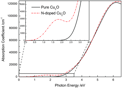 | ||
| Fig. 6 The calculated absorption coefficient as a function of photon energy of pure and N-doped Cu2O. | ||
4. Conclusions
Using first-principles calculations, the doping effects of nitrogen on the crystal structure, electronic structure, and optical properties of Cu2O have been systematically studied. Nitrogen impurities could be readily incorporated into the crystal lattice of Cu2O under O-poor conditions. For the crystal structure, nitrogen doping does not obviously change the lattice parameters of Cu2O, resulting in maintaining its original exceptional photoelectric performance. For the electronic structure, nitrogen doping slightly widens the band gap, and forms an IB in the gap located at about 0.9 eV from the VBM (or CBM). For the optical properties, nitrogen doping could generate new absorption peaks (in the region of 0.9–2 eV, corresponding to visible-light to near infrared in the solar light spectrum) below the band gap, resulting in enhancing the absorption ability for solar light. Based on these results, we considered that N-doped Cu2O is a perfect IB material for the novel kind of solar cells, owing to its suitable band gap and suitable position of the IB.Acknowledgements
The authors would like to acknowledge financial support from the National Natural Science Foundation of China (Grant No.21263006), Science Research Foundation of Educational Commission of Yunnan Province of China (Grant No. 2012Y542), and Introduced Talents Foundation of Kunming University of Science and Technology.References
- R. N. Briskman, Sol. Energy Mater. Sol. Cells, 1992, 27, 361 CrossRef CAS.
- Z. Zheng, B. Huang, Z. Wang, M. Guo, X. Qin, X. Zhang, P. Wang and Y. Dai, J. Phys. Chem. C, 2009, 113, 14448 CAS.
- S. Sahoo, S. Husale, B. Colwill, T.-M. Lu, S. Nayak and P. M. Ajayan, ACS Nano, 2009, 3, 3935 CrossRef CAS.
- F. L. Weichman, Phys. Rev., 1960, 117, 998 CrossRef CAS.
- S. Brahms, S. Nikitine and J. P. Dahl, Phys. Lett., 1966, 22, 31 CrossRef CAS.
- T. Minami, Y. Nishi, T. Miyata and J.-i. Nomoto, Appl. Phys. Express, 2011, 4, 062301 CrossRef.
- F. Caballero-Briones, J. M. Artés, I. Díez-Pérez, P. Gorostiza and F. Sanz, J. Phys. Chem. C, 2008, 113, 1028 Search PubMed.
- P. E. de Jongh, D. Vanmaekelbergh and J. J. Kelly, Chem. Commun., 1999, 1069 Search PubMed.
- W.-C. Huang, L.-M. Lyu, Y.-C. Yang and M. H. Huang, J. Am. Chem. Soc., 2012, 134, 1261 CrossRef CAS.
- M. Hara, T. Kondo, M. Komoda, S. Ikeda, J. N. Kondo, K. Domen, M. Hara, K. Shinohara and A. Tanaka, Chem. Commun., 1998, 357 RSC.
- A. Mittiga, E. Salza, F. Sarto, M. Tucci and R. Vasanthi, Appl. Phys. Lett., 2006, 88, 163502 CrossRef.
- G. P. Pollack and D. Trivich, J. Appl. Phys., 1975, 46, 163 CrossRef CAS.
- T. Minami, T. Miyata, K. Ihara, Y. Minamino and S. Tsukada, Thin Solid Films, 2006, 494, 47 CrossRef CAS.
- T.-J. Hsueh, C.-L. Hsu, S.-J. Chang, P.-W. Guo, J.-H. Hsieh and I. C. Chen, Scr. Mater., 2007, 57, 53 CrossRef CAS.
- B. D. Yuhas and P. Yang, J. Am. Chem. Soc., 2009, 131, 3756 CrossRef CAS.
- L. Gou and C. J. Murphy, Nano Lett., 2003, 3, 231 CrossRef CAS.
- K. Han and M. Tao, Sol. Energy Mater. Sol. Cells, 2009, 93, 153 CrossRef CAS.
- J. Cui and U. J. Gibson, J. Phys. Chem. C, 2010, 114, 6408 CAS.
- D. Li, C.-J. Chien, S. Deora, P.-C. Chang, E. Moulin and J. G. Lu, Chem. Phys. Lett., 2011, 501, 446 CrossRef CAS.
- J.-W. Chen, D.-C. Perng and J.-F. Fang, Sol. Energy Mater. Sol. Cells, 2011, 95, 2471 CrossRef CAS.
- W. Shockley and H. J. Queisser, J. Appl. Phys., 1961, 32, 510 CrossRef CAS.
- H. Raebiger, S. Lany and A. Zunger, Phys. Rev. B: Condens. Matter Mater. Phys., 2007, 76, 045209 CrossRef.
- X. Han, K. Han and M. Tao, Thin Solid Films, 2010, 518, 5363 CrossRef CAS.
- A. Luque, Phys. Rev. Lett., 1997, 78, 5014 CrossRef CAS.
- C. Malerba, C. L. Azanza Ricardo, M. D'Incau, F. Biccari, P. Scardi and A. Mittiga, Sol. Energy Mater. Sol. Cells, 2012, 105, 192 CrossRef CAS.
- S. Ishizuka, S. Kato, T. Maruyama and K. Akimoto, Jpn. J. Appl. Phys., 2011, 40, 2765 CrossRef.
- Y. Nakano, S. Saeki and T. Morikawa, Appl. Phys. Lett., 2009, 94, 022111 CrossRef.
- S. J. Clark, M. D. Segall, C. J. Pickard, P. J. Hasnip, M. J. Probert, K. Refson and M. C. Payne, Z. Kristallogr., 2005, 220, 567 CrossRef CAS.
- J. P. Perdew, K. Burke and M. Ernzerhof, Phys. Rev. Lett., 1996, 77, 3865 CrossRef CAS.
- V. I. Anisimov, J. Zaanen and O. K. Andersen, Phys. Rev. B: Condens. Matter, 1991, 44, 943 CrossRef CAS.
- B. G. Pfrommer, M. Câté, S. G. Louie and M. L. Cohen, J. Comput. Phys., 1997, 131, 233 CrossRef CAS.
- A. Werner and H. D. Hochheimer, Phys. Rev. B, 1982, 25, 5929 CrossRef CAS.
- C. G. Van de Walle and J. Neugebauer, J. Appl. Phys., 2004, 95, 3851 CrossRef CAS.
| This journal is © The Royal Society of Chemistry 2013 |
