 Open Access Article
 This Open Access Article is licensed under a Creative Commons Attribution-Non Commercial 3.0 Unported Licence
Plasma-enhanced chemical vapor deposition synthesis of vertically oriented graphene nanosheets
Zheng Bo
*a,
Yong Yang
b,
Junhong Chen
c,
Kehan Yu
d,
Jianhua Yan
a and
Kefa Cen
a
aState Key Laboratory of Clean Energy Utilization, Institute for Thermal Power Engineering, Zhejiang University, Hangzhou, Zhejiang 310027, China. E-mail: bozh@zju.edu.cn; Fax: +86 571 87951616; Tel: +86 571 87953055
bState Key Laboratory of Advanced Electromagnetic Engineering and Technology, Huazhong University of Science & Technology, Wuhan, Hubei 430074, China. E-mail: yangyong@hust.edu.cn
cDepartment of Mechanical Engineering, University of Wisconsin-Milwaukee, Milwaukee, Wisconsin 53211, USA. E-mail: jhchen@uwm.edu
dDepartment of Chemical Engineering, Case Western Reserve University, Cleveland, Ohio 44106, USA. E-mail: kxy108@case.edu
First published on 28th March 2013
Abstract
Vertically oriented graphene (VG) nanosheets have attracted growing interest for a wide range of applications, from energy storage, catalysis and field emission to gas sensing, due to their unique orientation, exposed sharp edges, non-stacking morphology, and huge surface-to-volume ratio. Plasma-enhanced chemical vapor deposition (PECVD) has emerged as a key method for VG synthesis; however, controllable growth of VG with desirable characteristics for specific applications remains a challenge. This paper attempts to summarize the state-of-the-art research on PECVD growth of VG nanosheets to provide guidelines on the design of plasma sources and operation parameters, and to offer a perspective on outstanding challenges that need to be overcome to enable commercial applications of VG. The review starts with an overview of various types of existing PECVD processes for VG growth, and then moves on to research on the influences of feedstock gas, temperature, and pressure on VG growth, substrate pretreatment, the growth of VG patterns on planar substrates, and VG growth on cylindrical and carbon nanotube (CNT) substrates. The review ends with a discussion on challenges and future directions for PECVD growth of VG.
 Zheng Bo | Zheng Bo is currently an associate professor at the State Key Laboratory of Clean Energy Utilization, Department of Energy Engineering, Zhejiang University (China). He received his PhD degree from Zhejiang University in 2008. During 2009 to 2011, he was a postdoctoral research associate at the University of Wisconsin-Milwaukee (USA). In 2011, he was awarded the National Excellent Doctoral Dissertation of China (Top 100). His research centers on non-thermal plasmas, and the design and synthesis of nanomaterials for energy and environmental applications. |
 Yong Yang | Yong Yang is currently an associate professor at the State Key Laboratory of Advanced Electromagnetic Engineering and Technology, Huazhong University of Science & Technology in Wuhan, China. He received his PhD degree in Mechanical Engineering from the Drexel Plasma Institute, Drexel University (Philadelphia, USA) in 2011. His research interests include the development, diagnostics and optimization of novel plasma sources at atmospheric pressure and their applications. |
 Junhong Chen | Junhong Chen received his PhD degree in Mechanical Engineering from the University of Minnesota in 2002, followed with postdoctoral research in Chemical Engineering at the California Institute of Technology. In 2003, he joined the University of Wisconsin-Milwaukee as an Assistant Professor in Mechanical Engineering, and was promoted to Associate Professor and Professor in 2008 and 2011, respectively. His current research interests include synthesis and assembly of nanoparticles, nanocarbons, and their hybrid nanomaterials for sustainable energy and environment (http://www.uwm.edu/~jhchen/). He is also the Director of NSF I/UCRC on Water Equipment & Policy and the founder of NanoAffix Science, LLC. |
 Kehan Yu | Kehan Yu is a postdoctoral scholar in the Sankaran group at Case Western Reserve University (USA). He received his BSc degree (2004) and MSc degree (2007) in Physics from Fudan University (China) and PhD degree (2012) in Mechanical Engineering from the University of Wisconsin-Milwaukee (USA). His research mainly focuses on carbon nanomaterials, especially on vertically oriented graphene, including synthesis and applications in photovoltaics, sensing and optoelectronics. |
 Jianhua Yan | Jianhua Yan, a Cheung Kong Scholar, is currently a professor at the State Key Laboratory of Clean Energy Utilization, Department of Energy Engineering, and working as the executive vice-president of the Graduate School of Zhejiang University (China). He received his PhD degree from Zhejiang University in 1990. He is currently the Chief Scientist of the National Program on Key Basic Research Project of China (973 Program). His research mainly focuses on environmental pollution control, energy conversion, and nanocatalysis. |
 Kefa Cen | Kefa Cen, an Academician of the Chinese Academy of Engineering, is currently a professor at the State Key Laboratory of Clean Energy Utilization, Department of Energy Engineering, Zhejiang University. He received his PhD degree from Moscow Industrial Technology University (USSR) in 1962. He is currently the Director of the Institute for Thermal Power Engineering of Zhejiang University, and the Director of the Teaching Steering Committee of Energy and Power Discipline of the Ministry of Education of China. His research mainly focuses on renewable energy, emission control, and nanotechnology. |
1 Introduction
The importance of the spatial alignment of one-dimensional (1D) nanostructures, such as nanowires, nanorods and nanotubes, to their applications has been well recognized.1–3 A well-known example is the vertically aligned carbon nanotube (CNT) array,4,5 which has been extensively demonstrated to show advantages over CNT powders and randomly oriented CNT mats in various applications such as field emitters, electromechanical actuators, gas sensors, and catalysis.6–10This ‘spatial alignment effect’ can be further extended to two-dimensional (2D) nanostructures, such as graphene, a lattice of sp2 carbon atoms densely packed into a hexagonal structure and covalently bonded along two planar directions.11,12 For surface-bound single layer graphene or stacks of graphene sheets, the orientation could be either horizontal or vertical, corresponding to graphene in parallel with or perpendicular to the synthesis/coating substrate, respectively. Vertically oriented graphene (VG) nanosheets, i.e., the so-called carbon/graphene nanowalls,13–34 carbon/graphene nanosheets,35–42 carbon/graphene nanoflakes,43,44 and carbon nanoflowers,45 are a class of networks of ‘graphitic’ platelets that are typically oriented vertically on a substrate. In these nanostructures, an individual VG nanosheet usually has lateral and vertical dimensions of 0.1 to tens of micrometers and a thickness of only a few nanometers (even less than 1 nm (ref. 46)). Each nanosheet consists of few-layer graphene with a layer number of 1–10 and an interlayer spacing of ∼0.34,17,47,48 to 0.35,26,49,50 0.36,36 or ∼0.37 nm.38,46 Compared with conventional horizontally oriented graphene, the rising interest in the application of vertically oriented graphene (VG) nanosheets initially stems from their unique orientation, exposed sharp edges, non-stacking morphology, and huge surface-to-volume ratio, etc. Until now, emerging applications of VG or its derivatives mainly include field emitters,30,38–40,44,46,51–60 atmospheric nanoscale corona discharges,49 gas sensors and biosensors,26,43,61 supercapacitors,21,35,45,62–64 lithium-ion batteries,42,47,65 fuel cells (catalyst supports),15,50,66 and electrochemical transducers.14 It is noteworthy that the above-mentioned applications usually call for different morphologies and structures of VG nanosheets. In the case of VG working as the electrode of atmospheric nanoscale corona discharges, exposed sharp edges and excellent electrical conductivity of graphene were key requirements for electric field enhancement, and meanwhile, a moderate intersheet/interlayer spacing was preferred for simultaneous improvement in the discharge current and minimization of the electrostatic screening effect.49 When VG was used as the active material of electric double-layer capacitors (i.e., the so-called supercapacitors) or lithium-ion batteries, a huge specific surface area was needed for possible massive ion loading, and the intersheet/interlayer spacing should be well adjusted to optimize the ion diffusion, adsorption, or intercalation aiming at a better energy storage performance.42,64 For the application of photovoltaics where the outstanding electrical conductivity of VG was used, a three-dimensional structure with highly branched nanosheet morphology could make it an excellent potential candidate for light scattering photoanodes.61,71 Finally, the high surface area and abundant surface defects have been demonstrated to benefit gas sensing applications.26,41 Consequently, broad applications of VG call for controllable growth of VG with desirable characteristics, which will be the main topic of the current review.
With a few exceptions that use glassy carbon or graphite sputtering59 and substrate sputtering72 techniques, chemical vapor deposition (CVD), especially the plasma-enhanced chemical vapor deposition (PECVD), has emerged as a key method for VG synthesis. Compared with thermal chemical vapor deposition (T-CVD) growth, PECVD offers the advantages of a lower substrate temperature, higher growth selectivity, and better control in nanostructure ordering/patterning,18,70,73–75 due to the presence of energetic electrons, excited molecules and atoms, free radicals, photons, and other active species in the plasma region, which make PECVD a popular method for VG growth. On the other hand, compared with T-CVD methods primarily based on neutral gas chemistry, growth of VG using PECVD is a more complex process,76 and the morphology and structure of the as-produced VG sheets are strongly influenced by both the plasma source and a series of operation parameters.
This review aims to summarize the state-of-the-art research on VG growth using PECVD, and to provide guidelines on the design of plasma sources and operation parameters. The first part of this review is an overview of various plasma sources and reactor configurations for VG growth. The next three sections are devoted to introducing the influences of various processing parameters, including the feedstock gas type and composition, the substrate temperature, and the operation pressure, on the plasma characteristics and the as-grown VG properties. Finally, deliberate treatment of substrates for controlled VG growth, VG pattern growth on convenient planar substrates, and VG growth on cylindrical and CNT substrates are introduced. The review concludes with a discussion on remaining challenges and future directions for PECVD growth of VG.
2 Plasma sources
Surface-bound VG nanosheets were initially discovered during the fabrication of CNTs in 1997, by direct current (dc) arc discharge evaporation of graphite in the presence of rarefied hydrogen gas.77 Since then, plasma sources with different power frequencies such as microwave (MW) plasma (f = 0.5–10 GHz; commonly 2.45 GHz),22,25,32,33,36,37,43,58,78–80 radio frequency (RF) plasma (f = 1–500 MHz; commonly 13.56 MHz),16,23,24,38,46,68–70,81 dc plasma,26,34,47,55,82,83 and their combinations,20,29,84–87 have been developed for VG synthesis. Besides gas discharge plasma sources, electron beam excited plasma22 has also been used for VG growth but with limited applications, and thus is not included in the current review.2.1 Microwave plasmas
MW plasma is a type of electrodeless gas discharge plasma with high frequency electromagnetic radiation in the GHz range. The wavelength of MW is in the centimeter range, which is comparable with the discharge system size, so the interaction between the electromagnetic field and the plasma in MW discharges is quasi-optical. For MW confined by a reflective boundary (i.e., the so-called waveguide), there are two typical wave propagation modes, i.e., transverse electric (TE) mode and transverse magnetic (TM) mode, referred to as the electric field and magnetic field perpendicular to the direction of wave travel, respectively.MW reactors of TE mode driven by a rectangular waveguide were used extensively for VG synthesis.22,58,78,88,89 As schematically shown in Fig. 1a, a 2.45 GHz MW source is coupled to the VG synthesis reactor vessel (a cylindrical quartz tube) via a traverse rectangular cavity waveguide. The incident electromagnetic wave formed in the waveguide interacts with the plasma generated in the discharge. This interaction results in partial dissipation, partial transmission and reflection of the electromagnetic wave.90 To increase the effectiveness of electromagnetic wave coupling with the plasma column, the transmitted wave can be reflected back, which leads to the formation of a standing wave. A tuner is used to adjust the waveguide length to make sure the standing wave electric field in the growth region is the strongest. Such special coupling techniques permit an increase in the fraction of the electromagnetic energy absorbed in the plasma, which is important for practical applications of the discharge system. The TE-MW reactor is able to synthesize VG with a relatively facile setup but, however, has the disadvantages of limited substrate temperature and the possible introduction of contamination from the outside container, since the wave is directly coupled to the quartz tube with a surface wave plasma mode. Furthermore, the operation power for VG synthesis using TE-MW reactors was limited to typically 60–500 W.22,58,78 A higher operation temperature and MW power could lead to the possible damage of the quartz tube and the vacuum system. In addition, the MW power cannot be easily confined and the spread of MW could lead to decreased growth efficiency and uniformity of the morphology and the structure of as-grown VG.
 | ||
| Fig. 1 Schematic diagrams of various PECVD systems for VG growth: (a) TE-MW (reprinted with permission from ref. 67; Copyright 2010 American Institute of Physics), (b) TM-MW (reprinted with permission from ref. 25; Copyright 2006 Elsevier), (c) ICP (reused with permission from ref. 68; Copyright (2004) Elsevier), (d) helicon plasma (reprinted with permission from ref. 24; Copyright 2006 Japan Society of Applied Physics), (e) CCP + ICP (reused with permission from ref. 69; Copyright 2005 Elsevier), (f) VHFCCP + MW (reprinted with permission from ref. 29; Copyright 2008 American Institute of Physics), (g) expanding CCP (reprinted with permission from ref. 70; Copyright 2010 Institute of Physics Publishing), (h) parallel-plate dc glow discharge plasma, and (i) pin-to-plate normal glow discharge plasma. | ||
A solution to the above problems is using the TM-MW reactor,25,33,36,37,43,50,79,80 where the dominant wave is converted from the TE mode in a rectangular waveguide to the TM mode in a cylindrical waveguide. As schematically shown in Fig. 1b, an antenna is introduced at the top of the VG synthesis reactor vessel, a cylindrical cavity, through a coaxial port, to produce a more intense electric field on the central part of the substrate where a plasma ball will be clearly observed. Different from the TE-MW reactor in which the substrate is immersed into the plasma region, the substrate of a TM-MW reactor is below the plasma ball and thus enables the possibility of a controllable substrate temperature. A dielectric window, usually a quartz plate, is positioned above the plasma in the TM-MW synthesis systems to avoid overheating,91 and thus allows higher operating power (2–3 kW) and pressure (several tens of Torr or several thousands Pa). The key internal discharge parameters, such as the charged-particle concentrations and the electron energy distribution function (EEDF), can be determined by Langmuir probe measurements. Experiments showed that a high-density (∼1012 cm−3) plasma can be produced at an operation power on the order of 1 kW.92,93
In some cases for both TE- and TM-MW systems, a dc bias (several hundreds of volts) is applied to the growth substrate by introducing a parallel plate58,78 to promote the growth and alignment of VG. The distance between the substrate and the parallel plate, as well as the in-series ballast-resistance, should be well adjusted to avoid the short circuit.
2.2 Radio frequency plasmas
Plasma driven at RF domain frequency is another popular power source for VG synthesis. There are three main modes to couple the energy of an RF generator to the plasmas: the evanescent electromagnetic (H) mode, the propagating wave (W) mode, and the electrostatic (E) mode.94H-Mode inductively coupled plasma (ICP) is based on the principle that the energy from the RF power is coupled by an inductive circuit element (typically a helical or spiral-like conductor) adjacent to or immersed inside the discharge region.95 The inductive coil stimulates the magnetic field in ICP discharges. The magnetic field further induces a high-frequency vortex electric field concentric with the elements of the coil, which is able to provide breakdown and sustain the inductively coupled discharge. The non-conservative electric field is relatively low, so the ICP plasma discharges usually operate at low pressures, where the reduced electric field E/p is sufficient for ionization.94
Generally, there are two main geometric designs for ICP reactors, i.e., the planar coil geometry and the cylindrical source tube with an expanding chamber.94 The former has been extensively applied for VG synthesis, where 13.56 MHz RF energy is inductively coupled through a quartz window into the deposition chamber through a 3-turn planar coiled RF antenna,16,38,68 as schematically shown in Fig. 1c. Based on the latter geometry, W-mode helicon (whistler wave) plasma is obtained by adding a helicon antenna to launch propagating electromagnetic waves, i.e., B0 as shown in Fig. 1d. Introducing a static magnetic field to an ICP-excited plasma will lead to a higher energy density and a larger plasma volume, and thus makes helicon reactors attractive for VG synthesis with a high growth rate. Typical magnetic field, RF frequency, and RF power values used for helicon plasma-assisted VG synthesis were 10 mT, 13.56 MHz, and 1000 W, respectively.24
E-Mode capacitively coupled plasma (CCP) can be produced by a pair of parallel plane electrodes separated by a small distance, with one electrode connected to the power supply while the other is grounded. Compared with ICP, the CCP with parallel-plane geometry takes advantage of simpler apparatus and a higher operation pressure. However, CCP working as an independent plasma source for VG synthesis is commonly considered not to be suitable,99,100 due to the relatively low electron density and electron energy. The plasma density and electron temperature of CCP (Langmuir probe measurements showed that the typical electron density was 109 to 1010 cm−3, and 1011 cm−3 for high-frequency CCPs101,102) are obviously lower than those of the above mentioned high-density plasma sources (1010 to 1012 cm−3 for microwave and ICP plasmas, and 1013 cm−3 for helicon plasmas).94,103 Meanwhile, the high sheath potential of CCP could possibly destroy the surface bonds and prevent the growth of high quality crystals.103,104 Contamination from the electrode is another potential issue. To our knowledge, the only successful application of CCP as an independent plasma source for VG growth was demonstrated by combining an expanding RF plasma with a magnetron sputtering setup, as shown in Fig. 1g, where the electron density could reach the level of 1011 cm−3 according to Langmuir probe measurement and, meanwhile, in this case the presence of nanostructured catalyst is an indispensable factor for successful growth of VG.17,70
As an alternative, CCP was used for VG synthesis in combination with other high-density plasma sources, such as CCP + ICP, and very-high-frequency (VHF) CCP + MW, as shown in Fig. 1e and f, respectively. The basic principle of these combinations is that the hydrocarbon (e.g., CH4) or fluorocarbon (e.g., CF4 and C2F6) gases are initially excited by a parallel-plate CCP to form CHx or/and CFx radicals (x = 1–3), while remote supplemental H radicals are provided by high-density plasma sources.99 This combination design takes advantage of the simultaneous formation of high density CHx/CFx radicals for large area synthesis and the sufficient production of H radicals for the removal of excess amorphous carbon (a-C). For CCP + ICP VG synthesis systems, typical RF frequencies and power for CCP and ICP were 13.56 MHz/100 W and 13.56 MHz/400 W, respectively.69 By adding a remote ICP H radical source, the H radical density can be increased by several times,85 which benefits the VG synthesis and further morphology control.23 Based on a similar principle, combination of CCP at VHF and MW was used for VG synthesis, where MW served as the high-intensity plasma source for H radical injection.20,29 CCPs at VHF can possibly lead to transition from the E- to the H-mode,94 benefiting the electron density and the operating pressure. For VHFCCP + MW VG synthesis systems, typical frequencies and power for VHFCCP and MW were 100 MHz/300 W and 2.45 GHz/250 W, respectively.29
2.3 Direct current plasmas
Petal-like carbon nanoroses obtained by dc arc discharge-assisted evaporation of graphite is commonly considered as the initial discovery of VG,77 while a better-aligned VG network was obtained by Obraztsov et al. using parallel-plate dc glow PECVD.82 Later research on VG synthesis mainly focused on dc glow discharges with different electrode arrangements.Parallel-plate dc glow, as schematically presented in Fig. 1h, is the commonly used dc PECVD practice for VG synthesis, taking advantage of its simple setup. When a sufficient potential is applied between planar cathode and anode, the so-called Townsend breakdown will occur. The minimum breakdown voltage for a particular gas composition, pressure and electrode distance can be expressed by Paschen's law.105 For a basic parallel-plate dc glow discharge, there are eight main regions distinguished from each other, along the direction from cathode to anode: Aston dark space, cathode glow, cathode dark space (cathode sheath), negative glow, Faraday space, positive column, anode glow, and anode dark space.103 The substrate is usually placed on the top of cathode (in some cases the substrate also serves as the cathode directly) since most of the applied potential difference drops in the first millimeters near the cathode, and the strong electric field and high ion flux within the cathode sheath are believed to benefit both the growth rate and the alignment of VG sheets during growth. For parallel-plate dc glow PECVD VG synthesis systems, the typical voltage and power were −50 to −250 V and 3 kW, respectively, and the interelectrode gap was usually several centimeters.55,98
Besides the parallel-plate style, dc glow PECVD synthesis of VG was also demonstrated using a pin-to-plate electrode pair.26,34 As schematically shown in Fig. 1i, a pair of asymmetric discharge electrodes, i.e., a sharpened tungsten tip and a planar substrate, is used. Benefiting from the highly enhanced electric field generated near the tungsten tip, the VG growth in the pin-to-plate dc PECVD system can be operated at atmospheric pressure with a relatively high growth rate, holding the potential for massive production. However, the inherently non-uniform characteristic of the pin-to-plate glow discharge plasma resulted in non-uniformity in both the morphology and the structure of as-grown VG sheets on the substrate.34 As suggested by Denysenko et al.,106 the effect of plasma non-uniformity can play a significant role in the PECVD process.
At the end of Section 2, we would like to present the as-reported Raman spectroscopy results of the VG obtained with different plasma sources. Raman spectroscopy is a fundamental and powerful tool for material characterization, which has been widely used to determine the structure and electronic properties of VG nanosheets. A typical Raman spectrum of VG nanosheets, as shown in Fig. 2a, presents fundamental peaks at ∼1350 cm−1 (D band, corresponding with the disorder-induced phonon mode and presents for the presence of disorders in the structure), ∼1580 cm−1 (G band, corresponding with the stretch vibration mode and presence of the graphitized structure), and ∼1620 cm−1 (D′ band, corresponding with the finite sp2 crystallite size), as well as three second order peaks at ∼2652 cm−1 (G′ or 2D band), ∼2915 cm−1 (D + G band), and ∼3240 (2D′ band).16,37,38,50,107 Most analyses on Raman spectrum of VG were focused on the shift and the FWHM of G and G′ peaks (sometime includes D and D′ peaks as well98) as well as the intensity ratio of the D-peak-to-G-peak I(D)/I(G). Generally, a higher I(D)/I(G) value and an increased FWHM value of the bands mean smaller crystalline grains as well as smaller inter-defect distance.108 The FWHM of the G band was reported as in the range of 22.5–77.01 cm−1 (22.5–60 for TM-MW PECVD,50,108 25–55 for TM-MW PECVD,33 39.3–43.2 for dc glow PECVD,98 and 40.28–77.01 for dc glow PECVD;34). Kurita et al. suggested that the size of as-grown VG can be estimated from the value of I(D)/I(G) where I(D)/I(G) decreases nearly linearly with the lateral length of an individual VG,98 as shown in Fig. 2b, which has been extensively confirmed by many researchers.16,34,38,109 It can be explained by the empirical equation proposed by Cancado et al., describing the relation among the in-plane sp2 crystallite size La, the excitation energy of laser source EL, and I(D)/I(G):110
 | (E1) |
 | ||
| Fig. 2 (a) Raman spectrum of VG nanosheets excited by 514 nm laser line; the insert shows the 1000–1800 cm−1 range, together with fitted peaks (reprinted with permission from ref. 107; Copyright 2006 American Institute of Physics). (b) The peak intensity ratio of the D-band to the G-band in the Raman spectrum as a function of the average length of VG nanosheets (reprinted with permission from ref. 98; Copyright 2005 American Institute of Physics). (c) The Raman spectrum of VG presenting a low peak intensity ratio of the D-band to the G-band (reprinted with permission from ref. 79; Copyright 2008 Institute of Physics Publishing). | ||
Some of the as-reported I(D)/I(G) values are: 0.2–0.3 for TM-MW PECVD (as shown in Fig. 2c, excitation 514 nm),79 0.3 for TM-MW PECVD (excitation 514.5 nm),33,109,111 0.35–1.11 for ICP (excitation 514 nm),38,112 0.65–0.93 for TM-MW (excitation 633 nm),50,108 0.77–2.66 for dc glow PECVD (excitation 532 nm),98 0.99 for TM-MW,25 1.35–2.43 for TE-MW (excitation 514 nm),107 and 2.39–3.28 for dc glow PECVD (excitation 633 nm laser).34 Details of the growth conditions of the above mentioned processes can be found in Table 1. It seems that the high-intensity plasmas tend to produce VG nanosheets with high degree of graphitization (relatively low I(D)/I(G) values). However, one should be very careful to make a general conclusion on which plasma source is the best choice by a simple comparison of I(D)/I(G) values. For example, the I(D)/I(G) value dramatically varies with the growth time even for the same plasma source, precursors, operation parameters, and Raman laser excitation.34 PECVD growth of VG is a very complex process and the plasma source is not the only critical parameter that determines the material quality. We will discuss other critical parameters influencing the material synthesis in the following sections.
| Plasma source | Precursor | Growth pressure/Pa | Substrate temperature/°C | Flow rate/sccma | Gas ratio | Ref. |
|---|---|---|---|---|---|---|
| a sccm: standard cubic centimetre per minute. b Catalyst was used. c Substrate with MW/RF CVD treatment. d Relative humidity: ∼40%. | ||||||
| Helicon | CH4 | 0.04–2 | 700 | — | — | 24 |
| ICP | CH4 | 12 | 630–830 | 10 | — | 68 |
| ICP | CH4/Ar | 0.3 | 400 | 30.4 | 16.4![[thin space (1/6-em)]](https://www.rsc.org/images/entities/char_2009.gif) :14 :14 |
23 |
| TM-MW | CH4/Ar | 17.33 | 450–500 | — | 1:8 |
36 |
| TM-MW | CH4/N2 | 5.32 × 10³ | 1250 | — | — | 50 |
| TM-MW | CH4/N2 | 5.32 × 10³ | >1000 | — | — | 43 |
| TM-MW | C2H2/N2/Ar | 1.33 × 10⁴ | 650–1050 | 200 | 0.5% C2H2 | 33 |
| TM-MW | CH4/N2/Ar | 1.33 × 10⁴ | 650–1050 | 200 | 4% CH4 | 33 |
| ICP | CH4/H2 | 12 | 630–830 | 10 | >1:9 |
68 |
| ICP | CH4/H2 | 2.66–53.2 | 600–950 | — | >1:19 |
96 |
| ICP | CH4/H2 | 13.33 | 700 | 10 | 2:3 |
38 |
| ICP | C2H2/H2 | 4–5.33 | 550–600 | 5 | 4:1 |
38 |
| TE-MW | CH4/H2 | 133 | 650–700 | 50 | 1:4 |
78 |
| TE-MW | CH4/H2 | 220 | 550 | — | 1:20 |
58 |
| TE-MW | CO/H2 | 250 | 700 | 50 | 23:2 |
22 |
| TM-MW | CH4/H2 | 5.32 × 10³ | 700 | 200 | 1:8 |
79 |
| TM-MW | CH4/H2/Ar | 1.33 × 10⁴ | 650 | 44 | 1:1:20 |
80 |
| TM-MW | C2H2/NH3 | 1.33 × 10³ | — | — | >1:1 |
25 |
| TE-MWb | CH4/CO2 | — | 900 | — | 53:47 |
89 |
| Expending CCPb | C2H2/H2/Ar | — | 700 | 1076 | 1:25:1050 |
70 |
| CCP + ICP | CH4/H2 | 13.3 | 500 | 45 | 1:2 |
69 |
| CCP + ICP | CF4/H2 | 13.3 | 500 | 45 | 1:2 |
69 |
| CCP + ICP | CHF3/H2 | 13.3 | 500 | 45 | 1:2 |
69 |
| CCP + ICP | C2F6/H2 | 13.3 | 500 | 45 | 1:2 |
69 |
| VHFCCP + MW | C2F6/H2 | 13.3–1596 | 600 | 150 | 1:2 |
29 |
| VHFCCP + MW | C2F6/H2/N2 | 13.3–1596 | 600 | 155 | 10:20:1 |
20 |
| VHFCCP + MW | C2F6/H2/O2 | 13.3–1596 | 600 | 155 | 10:20:1 |
80 |
| DC glow | CH4/H2 | 1 × 10⁴ | 1000 | — | 1:9 |
97 |
| DC glow | CH4/H2 | 9975 | 1000 | — | 8:92 |
83 |
| DC glowc | CH4/H2 | 2.66 × 10⁴ | 900–1000 | 50 | 3–8% CH4 | 87 |
| DC glowb | CH4/H2/Ar | 1.3 | 550–800 | 87 | 1:1.25:5 |
98 |
| DC glow | CH4/H2O/Ar | 1.01 × 10⁵ | 700 | 1500 | 10% CH4d | 34 |
3 Precursors
With a few exceptions of using metal–organic precursors, e.g., evaporated aluminum acetylacetonate (Al(acac)3),16 feedstock gases of most PECVD processes for VG synthesis are listed in Table 1, where the corresponding operating conditions are also presented. It was revealed by extensive work that the feedstock gas composition and proportion significantly affect plasma properties and synthesis processs, as well as the morphology and structure of the as-grown deposits.22,24,25,33,50,58 In this section, we will first discuss the roles of each feedstock gas component in the synthesis process, and then present the effect of feedstock gas proportion on plasma chemistry and VG growth.3.1 Carbon sources
Hydrocarbon (C2H2 or CH4) and fluorocarbon (CF4, CHF3 or C2F6) were the popular choices of carbon sources for most PECVD systems. Other particular cases mainly include: Mori et al. performed VG growth in a TE-MW system with a CO/H2 precursor,88 and Chatei et al. conducted the growth of VG using a TE-MW reactor with a mixture of CH4/CO2 where both CH4 and CO2 could be carbon sources simultaneously.89CHx (x = 1–3) radicals were believed to play an important role in the VG synthesis. Shiji et al. conducted comparative work on the VG synthesis in a CCP + ICP system with CH4 and a series of fluorocarbons diluted by H2, and they found that VG was successfully synthesized when CH4, CF4, CHF3 or C2F6 were used as the carbon source, but was not obtained with using the C4F8/H2 precursor.69 They further compared the as-grown VG morphology, including the growth rate, thickness, and inter-sheet spacing, for different carbon sources. The main observation included: VG grown using the CH4/H2 system was rather wavy while VG obtained using fluorocarbon/H2 precursors showed maze-like morphology, as shown in Fig. 3a; the interlayer spacing was in the order of CF4 > CHF3 > C2F6 > CH4, from large to small, as shown in Fig. 3a–d; and the growth rate was on the order of C2F6 > CHF3 > CH4 > CF4, from high to low, as shown in Fig. 3e. It is worth noting that the as-reported growth rate of VG (∼0.18 μm h−1 for C2F6/H2, ∼0.16 μm h−1 for CHF3/H2, ∼0.15 μm h−1 for CH4/H2, and ∼0.11 μm h−1 for CF4/H2) is much lower than those obtained in TM-MW (∼96 μm h−1 for CH4/N2),43 helicon (∼18 μm h−1 for CH4),24 ICP (∼16 μm h−1 for C2H2, ∼10 μm h−1 for C2H2/H2, and ∼2 μm h−1 for CH4/H2),38,68 TE-MW (∼15 μm h−1 CH4/H2),58 and dc glow (∼1.5 μm h−1 for CH4/H2)82 systems.
 | ||
| Fig. 3 SEM images of VG grown for 8 hours using (a) the CH4/H2 system, (b) the CF4/H2 system, (c) the CHF3/H2 system, and (d) the C2F6/H2 system. (e) VG growth height as a function of growth time for different systems. Information on plasma type and growth conditions can be found in Table 1. Reused with permission from ref. 69. Copyright 2005 Elsevier. | ||
Obraztsov et al. suggested that the presence of reactive carbon dimers (C2) could play a crucial role in VG growth.97Fig. 4 shows the optical emission spectroscopy (OES) measurement results obtained in a dc glow plasma system employing pure H2 and CH4/H2 mixtures. It was found that recombination lines of the atomic (656 nm, Hα; 487 nm, Hβ) and molecular (550–650 nm, H2) hydrogen dominate the emission spectrum when pure hydrogen was used as the feed gas, while the characteristic emission lines of CH radicals (390 and 430 nm) and C2 dimers (515 and 560 nm) were obviously observed, especially at areas near the growth substrate. Based on the OES results and the empirical calculations proposed by Gruen,113 they deduced the significant role of C2 in the evolution of critical nuclei into VG sheets with the insertion of C2 into the acetylene-like C![[double bond, length as m-dash]](https://www.rsc.org/images/entities/char_e001.gif) C bond to produce a carbene structure.97
C bond to produce a carbene structure.97
 | ||
| Fig. 4 Typical OES for pure hydrogen (a) and for a hydrogen–methane gas mixture with 10% (b) and 25% (c) of methane. Total gas pressure is 80 Torr (∼1 × 10⁴ Pa), applied voltage is 650 V (a), 750 V (b), and 850 V (c). The discharge current is 7 A (a), 6 A (b), and 5 A (c). Information on plasma type and growth conditions can be found in Table 1. Reused with permission from ref. 97. Copyright 2003 Elsevier. | ||
The important role of C2 in VG growth, especially for the formation of critical nuclei, was mentioned by many groups.33,38,50,70,88 C2 radical density of 1011 to 1013 cm−3 was demonstrated in the MW and ICP systems employing a CH4/H2 or CH4/H2/Ar mixture.114–116 Teii et al. conducted plasma diagnosis and material characterization on a TM-MW plasma (employing C2H2/N2/Ar or CH4/N2/Ar) as well as the as-grown deposits.33 As shown in Fig. 5a and b, the deposits from C2H2/N2/Ar were networks of VG while the deposits from CH4/N2/Ar consisted of VG intercepted by diamonds, which was attributed to the different C2 density in these two precursor systems.33 They further proposed different pathways for C2H2 and CH4 in their transformation to C2, i.e., C2H2 was able to produce C2 through direct dissociation due to the strong C![[triple bond, length as m-dash]](https://www.rsc.org/images/entities/char_e002.gif) C bond while CH4 was easily converted to CHx (x = 1–3) radicals to produce C2 through radical recombination and subsequent dissociation. This explained the absence or near absence of diamonds in the deposits of C2H2/N2/Ar system, where a higher C2 radical density facilitated the formation of non-diamond carbon components including microcrystals of graphite, carbides, and amorphous carbon (a-C).117 Very recently, Teii et al. proposed the growth regimes for nanodiamond and VG, as shown in Fig. 5c, and concluded that VG grew from C2 and unsaturated radicals. However, the as-proposed growth regime of VG is not a universal conclusion since the growth of VG without the formation of diamond at a lower substrate temperature has been extensively demonstrated using other systems (see Table 1).20,22–24,29,33,34,36,38,58,68,69,78–80,89,96,98
C bond while CH4 was easily converted to CHx (x = 1–3) radicals to produce C2 through radical recombination and subsequent dissociation. This explained the absence or near absence of diamonds in the deposits of C2H2/N2/Ar system, where a higher C2 radical density facilitated the formation of non-diamond carbon components including microcrystals of graphite, carbides, and amorphous carbon (a-C).117 Very recently, Teii et al. proposed the growth regimes for nanodiamond and VG, as shown in Fig. 5c, and concluded that VG grew from C2 and unsaturated radicals. However, the as-proposed growth regime of VG is not a universal conclusion since the growth of VG without the formation of diamond at a lower substrate temperature has been extensively demonstrated using other systems (see Table 1).20,22–24,29,33,34,36,38,58,68,69,78–80,89,96,98
 | ||
| Fig. 5 SEM images of the deposits obtained on Si substrates in (a) CH4/N2/Ar (4:10:86) at a deposition temperature of 1150 °C, and (b) C2H2/N2/Ar (0.5:29.5:70) at a deposition temperature of 950 °C (reprinted with permission from ref. 33; information on plasma type and growth conditions can be found in Table 1, copyright 2009 American Institute of Physics), (c) variation of the deposits as a function of substrate temperature and gas composition. MD: microcrystalline diamond; ND: nanodiamond; CNWs: carbon nanowalls (VG). Reprinted with permission from ref. 109. Copyright 2012 IEEE. | ||
Zhu et al. compared the growth of VG in an ICP system employing CH4/H2 and C2H2/H2 precursors.38,96 VG growth using C2H2/H2 ICP had a higher growth rate, and meanwhile, the as-grown VG sheets presented more ordered vertical orientation and more uniform sheet height distribution, compared with the CH4/H2 counterpart, as shown in the top view and side view SEM images in Fig. 6a–d. Meanwhile, the edge thickness of a single VG nanosheet obtained by C2H2/H2 growth was about 1–2 nm (3–4 atomic layers as shown in the TEM image in Fig. 6e), which was slightly larger than that of CH4/H2 growth (<1 nm as shown in the SEM image of Fig. 6f). The growth temperature could be lowered by 100–150 °C when using C2H2 instead of CH4 as a feedstock. They attributed the above observation to the higher carbon-bearing species density in the plasmas employing C2H2 feedstock due to the lower dissociation energy.96 It is worth noting that the use of C2H2 could possibly induce short-circuit risk for some PECVD systems due to the easy production and deposition of a-C in an uncontrolled manner.
 | ||
| Fig. 6 (a) Top view SEM image of VG nanosheets deposited on a Si substrate using 80% C2H2 in H2, at 600 °C substrate temperature, 35 mTorr (4.66 Pa) total pressure, and 1000 W RF power for 10 min. Inset: enlarged SEM image shows the edge thickness of 1–2 nm. (b) Side view SEM image of the C2H2 VG nanosheets shown in (a). (c) Top view SEM image of typical (40% CH4 in H2, 700 °C, 100 mTorr (13.3 Pa), and 900 W) CH4 VG nanosheets deposited on a Si substrate for 20 min. (d) Side view SEM image of the CH4 VG nanosheets shown in (c). (e) HRTEM micrograph of C2H2 VG nanosheets grown directly on a Cu grid. Inset: selected area electron diffraction pattern of the same nanosheet. Reused with permission from ref. 38. Copyright 2011 Elsevier. (f) SEM image of an enlarged CH4 VG nanosheet. Information on plasma type and growth conditions can be found in Table 1. Reused with permission from ref. 96. Copyright 2007 Elsevier. | ||
Vizireanu et al. suggested that ionic clusters of carbon CnH+x (n ≥ 2, x = 1, 2, 3) are the building species for VG nanosheet growth, based on their OES and mass spectroscopy measurements on a RF expanding plasma and the morphology characterization of the as-grown VG nanosheets.70 As shown in Fig. 1g, the employed RF expanding plasma allowed the easy adjustment of the distance between the substrate and the gas injection point, and thus facilitated the investigation on the plasma chemistry involving both the species transported from the interelectrode space and those locally generated.70Fig. 7a shows the mass spectrum of the ions sampled from plasma, recorded at 5 cm from the injection point, where the quality of the VG nanosheets was considered as the highest, compared with those obtained closer to or farther from injection. Correspondingly, as shown in Fig. 7b, although generally the intensities of C2, CH, H and Ar species decreased along the flow with an increasing distance from the injection, it was observed that there was an enhancement of radical emission at the region around 5 cm (see the inset of Fig. 7b). The mass spectrum intensities of H+x and CH+x species decreased along the flow but those of ionic clusters of carbon CnH+x (n ≥ 2, x = 1, 2, 3) presented a maximum value at around 5 cm, as shown in Fig. 7c and d. The electron density and plasma potential were measured by Langmuir probe as 3.5 × 10¹⁷ m−3 and 43 V, respectively. They further proposed a possible mechanism for the formation of a high-mass ionic cluster of carbon, including the formation of low-mass ions from the reactions induced by background Ar and H2 ions/molecules as well as energetic electrons, and the ionic chain polymerization process.70
 | ||
| Fig. 7 (a) The mass spectrum of the ions sampled from plasma, recorded at 5 cm from the injection point. (b) Dependence of emission intensities of C2, CH, H and Ar species as a function of distance. Inset: dependence upon position of the ratio of local C2, CH, H intensities to the local intensity of Ar line. The dependence of the concentration of various ionic species upon the distance from the injection (c) H+x and CH+x species and (d) ionic clusters of carbon CnH+x (n ≥ 2, x = 1, 2, 3). Information on plasma type and growth conditions can be found in Table 1. Reprinted with permission from ref. 70. Copyright 2010 Institute of Physics Publishing. | ||
In Mori et al.'s CO/H2 TE-MW system, a strong C2 Swan band and a Balmer α line of atomic hydrogen were observed in their OES measurements, both of which were considered to be critical to the growth of VG.88 They suggested the important role of C2 in VG growth, and further deduced a possible C2 formation pathway involving C, C2O and CO.
3.2 Amorphous carbon etchants
Although some details on the complex plasma chemistry in the VG growth process have yet to be fully revealed, it has been widely accepted that a basic VG growth evolution consists of the initial nucleation, the subsequent formation of VG nanosheets from the nuclei, and the further vertical growth.25,34,86,96 The effective removal of a-C was widely recognized as a crucial and inevitable step to the formation of high quality nanoislands during the initial nucleation stage.Possible a-C removal species could be atomic hydrogen, excited nitrogen species, atomic oxygen, and hydroxyl radicals, as reported by different groups using various precursors and plasma sources. Hiramatsu et al. applied CCP + ICP and VHFCCP + MW systems with a mixture of hydrocarbon/H2 or fluorocarbon/H2 to grow VG, and their work suggested that it was H atoms that play the most significant role in the removal of undesirable amorphous phases; H atoms were also believed to extract bonding atoms from the gas-phase radicals migrating on the growing surface or edge of graphene layers (e.g., F from CFx radicals when fluorocarbon/H2 was used as the precursor).23,29,69,118 Similarly, Zhu et al. explored the growth mechanism for VG synthesis by ICP and they found that H atoms acted as an effective etchant to rapidly remove a-C defects due to the different etching rates of H atoms to a-C, sp2 and sp3 hybridized carbon, benefiting both the crystalline graphitic structure and the sharp edges in the growth layers.96 Chuang et al. used a TM-MW reactor to synthesize freestanding VG, with a mixture of C2H2/NH3, where NH3 served as the H atom source for a-C removal.25 Shang et al. reported the growth of VG using a TM-MW system with a mixture of CH4/N2, and they suggested the advantage of nitrogen in etching the a-C phase compared with hydrogen.43 Kondo et al. investigated the initial growth process of VG for the conditions with and without O2 gas addition to a C2F6/H2 VHFCCP + MW system, and they found O2 addition has the effect of reducing a-C and controlling VG nucleation.86 Chatei et al. compared the as-grown VG using CH4/CO2 or CH4/H2 in a TE-MW reactor, and concluded that OH radicals and O atoms have a stronger ability to etch a-C than H atoms.89 Bo et al. applied a dc pin-to-plate negative normal glow PECVD reactor for the synthesis of VG under atmospheric pressure, and it was found OH radicals with an adequate concentration would benefit the etching of a-C and the growth of VG.34
With the use of a high-intensity plasma source such as helicon, ICP, or TM-MW, VG growth can be realized using pure CH4 as the feedstock gas, where CH4 serves as the carbon source and the a-C etchant simultaneously. Sato et al. used a helicon discharge, capable of producing plasmas with a high concentration of electrons (∼1011 cm−3, according to Langmuir probe measurements as shown in Fig. 7a) and highly energized ions, to synthesize VG using CH4 without dilution.24 As shown in Fig. 8b, strong optical emission lines of 656.2 nm of Hα, 486.1 nm of Hβ, and 431.5 nm of CH were observed in the OES measurement on the CH4 helicon plasma for a 3 mT magnetic field, indicating both the large volume and highly energetic H atoms. Wang et al. demonstrated VG growth in an ICP system using pure CH4 as the precursor.68 They further conducted OES measurements on the plasmas produced by ICP and CCP reactors and found a dramatic increase in the intensity of H atom peaks from the ICP reactor relative to the CCP reactor.100 The above practice employing relatively high-intensity plasmas ensures the sufficient formation of H atoms from the disassociation of CH4 (without dilution), and allows the efficient a-C removal for further growth of VG, where the pure hydrocarbon serves as the carbon source and the a-C etchant simultaneously. Besides the above practices using pure carbon source as the precursor, successful VG growth was also demonstrated in ICP and TM-MW systems using a mixture of carbon source gas and argon as the feedstock gases.36,81 Argon was not considered as an a-C etchant but has the ability to enhance the electron energy and favors plasma stability. The role of argon in the PECVD process will be discussed in detail in Section 3.3.
 | ||
| Fig. 8 (a) Plasma density dependence on gas pressure for a 3 mT magnetic field. (b) Typical visible emissions from CH4 helicon plasma for 3 mT magnetic field. Information on plasma type and growth conditions can be found in Table 1. Reprinted with permission from ref. 24. Copyright 2006 Japan Society of Applied Physics. | ||
Besides the above mentioned PECVD processes that employing pure hydrocarbon as the precursor, a more common way to make sure of the sufficient production of a-C removal species was via introducing additional a-C etchant sources, such as hydrogen-rich gases (e.g., H2 and NH3),22,25,29,33,43,50,58,68,69,78–80,96–98 oxygen-rich gases (e.g., O2 and CO2),86,89 and hydroxyl-rich gas (e.g., H2O),34 into the precursor. These gas additions are especially desired for CCP or dc plasmas of relatively low intensity, where the shortage of a-C removal species from the direct disassociation of carbon sources is obvious. Bo et al. conducted OES measurements on an atmospheric dc pin-to-plate negative normal glow PECVD reactor in CH4/Ar, CH4/Ar/H2, and CH4/Ar/H2O, and compared the corresponding as-grown deposits.34 As shown in Fig. 9a, only emissions from CH radicals (314 nm, C2Σ+a − X2Π; 388 nm, B2Σ−a − X2Π; 431 nm, A2Δ − X2Π), C2 radicals (516 nm, A3Πg − X3Πu), and Ar atoms (697 nm, 707 nm, 727 nm, 738 nm, 750 nm, 764 nm, 772 nm, and 795 nm) were identified for the CH4/Ar discharge, and there was only carbon black but no VG was produced. By adding H2 into the system (40% H2 by volume), Balmer transition of H atoms (656 nm, Hα; 487 nm, Hβ; 434 nm, Hγ) was observed, as shown in Fig. 8b, and accordingly VG was observed in the as-grown deposits but with a quite low growth rate. The above observation was attributed to the shortage of H atoms due to the relatively short mean free path of electrons or low electron energy in the atmospheric glow discharge. With H2O addition, emissions from OH radicals (309 nm, A2Σ+ − X2Π; 434 nm, C – B) and H atoms (656 nm, Hα) were observed, as shown in Fig. 9c, where VG sheets were synthesized at a relatively high rate.
 | ||
| Fig. 9 Optical emission spectra for the normal glow discharge systems of (a) CH4/Ar, (b) CH4/Ar/H2, and (c) CH4/Ar/H2O at a supply voltage of 3.35 kV and an interelectrode gap of 10 mm. The lower spectrum (red) in each panel was obtained by subtracting the background signal without discharge (blue) from the total spectrum with discharge (black) to eliminate the luminous emission contribution from the heated furnace. Information on plasma type and growth conditions can be found in Table 1. Reprinted with permission from ref. 34. Copyright 2011 Elsevier. | ||
Another approach to produce a-C removal species is to use combined plasma sources. The so-called ‘radical injection’ technique was thus proposed with coupling high-intensity plasma sources such as ICP or MW, capable of effectively producing large amounts of H atoms, to the CCP or VHFCCP system.29,69 As briefly mentioned in Section 2.2, CCP or VHFCCP is used to produce large amount of CHx/CFx radicals for large area synthesis, while the role of remote ICP or MW is providing H radicals as an individual high-intensity plasma source. An important advantage of this technique is that it provides an active method to control the composition of radicals in the reaction field, since CHx/CFx and H radicals are produced by separate plasma sources, benefiting the controllable growth of VG nanosheets.118
3.3 Argon
Ar was introduced into many PECVD processes mainly based on the following reasons.First, Ar has a relatively high excitation and ionization potential (with first excitation potential at 11.55 eV and ionization potential at 15.76 eV).119 This means that the interaction between electrons and Ar atoms is mostly dominated by elastic collisions and the loss of electron energy through inelastic collisions (mainly vibrational excitation), which is the major energy transfer pathway in molecular gas environment, can be significantly reduced. This effect would make the electrons retain their energy, leading to an increase in average electron temperature. Consequently, the addition of Ar to carbon source and a-C etchant produces a plasma capable of providing electrons of elevated energy and the necessary level of ionization rate, which would enhance the PECVD process. This feature will further improve the plasma stability.
Another advantage of Ar addition is that it could enhance the formation of critical species for VG growth, i.e., C2, H, and ionic clusters of carbon CnH+x (n ≥ 2, x = 1, 2, 3). Goyette et al. detected the presence of gas phase C2 and calculated its column density in an MW PECVD system with CH4/H2/Ar, and they found that a high fraction of Ar favored the formation of C2 as well as H atoms.115 Teii et al. performed OES measurements on a TM-MW plasma and suggested a C2 formation route via the direct dissociation reaction with gaseous feedstock, e.g.:33
| C2H2 + Ar → C2 + H2 + Ar | (R1) |
They found that a higher Ar concentration enhances the C2 production, benefiting the high degree of graphitization on the surface at a relatively low temperature. As shown in Fig. 10, the VG (i.e., labeled as CNW in the Figure) the growth temperature decreases from 1000 to 650 °C with increasing Ar concentration from 30% to 70%.33,117 Vizireanu et al. suggested that the presence of Ar ions and metastables could help the production of C2H2 molecular ions excited on vibrational and rotational levels and the formation of H atoms:70
| C2H2 + Ar+,m → C2H2+,* + Ar | (R2) |
| H2 + Ar → ArH+ + H | (R3) |
| H2 + Ar → Ar + H+ | (R4) |
 | ||
| Fig. 10 Dependence of deposition temperature on the Ar concentration for Ar/N2/C2H2 TM-MW plasma. Reprinted with permission from ref. 33. Information on plasma type and growth conditions can be found in Table 1. Copyright 2009 American Institute of Physics. | ||
The subsequent formation of higher mass clusters, which were considered as the building species for VG nanosheet growth (as aforementioned in Section 3.1), could be realized via the polymerization process involving C2H2+ and other low mass ions such as C2H+, C2+, CH+, and CH+2, etc.70
Ar also takes advantage of high stability and extremely low reaction rate, benefiting the purity of the as-grown materials. Finally, Ar is abundant and therefore more inexpensive than other noble gases such as He.
3.4 Nitrogen
N2 can work as an efficient a-C etchant in the PECVD systems for VG growth. Soin et al. and Shang et al. reported synthesis of VG using a TM-MW plasma reactor with the feedstock gas of CH4/N2 mixture.50,120 Both studies indicated the advantage of using N2 instead of H2 in the removal of excess a-C.43,50,108 Shang et al. reported successful ultrafast growth of VG nanosheets using CH4/N2 precursor in a TM-MW reactor at a temperature higher than 1000 °C, and they attributed the high growth rate of 96 μm h−1 partially to the stronger a-C etching ability of N2.43 It has been mentioned in the literature on PECVD growth of CNTs121 and diamond films122 that N2 can promote the dissociation of CH4 to lose H atoms and to form C2 and CN species, both of which were observed in N2-containing PECVD systems for VG growth.33Meanwhile, the N2 addition will change the morphology and structure of the as-grown VG by substituting C atoms and will introduce additional defects. Takeuchi et al. conducted research on the comparison of electrical conduction between undoped and N-doped VG samples.20 It was found that with N2 addition, the as-grown VG shows less alignment and highly branching morphology, but there was no obvious difference in the height and interlayer spacing.
Compared with the slight variation of morphology, the electrical conduction type presented a dramatic change with a transition from p-type for undoped VG to n-type for N-doped VG. As shown in Fig. 11, the resistivity and Hall coefficient of the undoped VG were obviously higher than those of the N-doped VG; the carrier (electron) concentration increased with an increase of N2 concentration for the n-type N-doped VG; the charge mobility of the N-doped VG was higher than that of the undoped VG, but decreased with a further increase in the N2 concentration. This observation was further confirmed by Teii et al.'s Hall- and Seebeck-effect measurements.33 It thus provides an alternative for electrical conduction control on the as-grown VG, providing the potential for functional device applications. The manipulation of transport properties in VG can pave the way to the applications for chemical sensing, transistor, and conductive thin films.
 | ||
| Fig. 11 Variations in (a) Hall coefficients and resistivity, (b) carrier concentration and N content in VG, and (c) Hall mobility as a function of N2 flow rate during the growth process. Information on plasma type and growth conditions can be found in Table 1. Reprinted with permission from ref. 20. Copyright 2008 American Institute of Physics. | ||
3.5 Gas proportion
The gas proportion plays a significant role in the VG synthesis. It is not only capable of, to a certain extent, determining the type of the final deposits (e.g., a-C, CNTs, diamond, and/or VG), but also strongly influences the morphology and structure of the as-grown VG.Wu et al. reported a series of deposits obtained for the same CH4/H2 TE-MW system with different gas ratios.13 As shown in Fig. 12a–f, carbon structures of a-C, VG sheets, CNTs/carbon nanofibers, 2D nanographite sheets, and the columnar structure of a-C were obtained with an increasing H2 concentration. Further increase of H2 concentration to a rather high value will lead to the formation of diamonds. Wang et al. studied the influence of CH4 concentration in a CH4/H2 mixture on the VG growth performance in an ICP system.68 A high CH4 concentration will lead to a high nucleation tendency and consequently decrease the sheet lateral size and meanwhile increase the VG density, as shown in Fig. 12g–i. It is hard to define a certain optimum feedstock gas ratio for all the PECVD systems, even of the same type, due to the difference in plasma characteristics and operating conditions. Generally for CH4/H2 PECVD systems, a gas ratio of CH4:H2 larger than 1:20 will be suitable for the growth of VG, rather than the formation of CNTs, diamond, or other nanostructures.
 | ||
| Fig. 12 SEM images of the deposits obtained from a TE-MW system at different H2/CH4 flow rate ratios: (a) 30, (b) 15, (c) 10, (d) 6, (e) 4, (f) 1. Scale bars: (a), (b), (d), and (f) 1 mm; (c) and (e) 100 nm. (Reprinted with permission from ref. 13. Copyright 2004 Royal Society of Chemistry.) SEM images of VG grown with an ICP reactor at different CH4 concentrations on Si substrates: (g) 10% CH4; (h) 40% CH4; (i) 100% CH4 in an ICP system. RF power: 900 W, deposition temperature: 680 °C, pressure: 12 Pa, growth time: 20 min. (Reused with permission from ref. 68. Copyright 2004 Elsevier.) Information on plasma type and growth conditions can be found in Table 1. | ||
The proportion of the a-C etchant source in the precursor is a very important parameter for the VG growth, where its dual effects on the VG growth should be well balanced.
Taking the CH4/H2 system for example, H atoms will etch a-C, sp2 and sp3 hybridized carbon simultaneously with different etching rates, which means it will promote the formation of nanoislands for initial nucleation and meanwhile bombard the as-grown VG sheets. Consequently, the number of layers in the as-grown VG sheet network decreased from 8–10 to 2–4, as reported by Zhang et al. for their CH4/H2 TE-MW system.58 A similar observation was obtained when H2O was used as the etchant. Bo et al. studied the influence of H2O content on the morphology and structure of the VG grown by an atmospheric normal glow discharge.34 For a relatively low relative humidity value of 18.9%, as shown in Fig. 13a, very few nanoislands (highlighted by red circles) were formed indicating poor initial nucleation of VG; however, the lateral size of some VG layers (highlighted by blue circles) could reach ∼500 nm. On the contrary, as shown in Fig. 13c, a relatively high relative humidity value of 62.1% led to the formation of nanoislands of high density while very few large VG layers were observed. If the concentration of OH radicals reaches a certain high level, it will also prevent the subsequent formation of graphitic fragments and VG nanosheets most likely due to undesirable oxidation erosion.
 | ||
| Fig. 13 SEM images of the deposits formed in the discharges with different H2O addition ((a): relative humidity = 18.9%; (b): relative humidity = 38.8%; (c): relative humidity = 62.1%). Red circles in (a): nanoislands; blue circles in (a): large size nanosheets. Information on plasma type and growth conditions can be found in Table 1. Reprinted with permission from ref. 34. Copyright 2011 Elsevier. | ||
An over-high relative humidity value (such as ∼80%) could significantly degrade the stability of the glow discharge. An optimum relative humidity of ∼40% was reported for the system with the best morphology of VG layers, as shown in Fig. 13b.
4 Temperature
Thermal and electrical energy are introduced into the PECVD system with the forms of heat and plasma, respectively. VG growth by PECVD process usually can be operated at a relatively lower temperature compared with those using T-CVD, due to the presence of energetic electrons and active species in the plasma. With good control of the plasma chemistry, the growth temperature could be lowered. As mentioned in Section 3.3, VG growth can be realized at a lower temperature with a higher Ar introduction.33Most PECVD VG growth processes used external resistive heating on the substrate, except MW PECVD systems where the microwave leads to substrate heating. The interaction between low-temperature plasmas and solid substrate surface includes both the thermal and the momentum transfer,123 which means the plasmas, especially high-intensity ones, will not only provide heat for the substrate but also possibly lead to an ion-etching on the substrate surface. Krivchenko et al. carried out a seeding process on the substrate in a MW/RF CVD device, for the subsequent VG growth using dc glow PECVD.87 It was found that the treated surface was ion-etched and led to the formation of active surface defects. For atmospheric dc negative normal glow discharges, not only the substrate but also the precursors should be heated and thus a furnace was used.34 Generally, the amount of energy input for dc glow discharge is limited to avoid the glow-to-arc transition.124 The low input energy level could lead to lower electron density and electron temperature. On the other hand, microwave or RF systems are capable of generating plasmas at high power and temperature levels. Consequently, compared with MW or RF plasmas, the DC glow discharge usually relies on external heating to achieve similar effects as other high-energy plasma systems.
Substrate temperature is very important to the PECVD process since it strongly affects the surface reaction kinetics.125 It is believed that a higher substrate temperature offers more species for nucleation and thus favors VG growth rate.96 Generally, the substrate temperature should be heated to at least 500–650 °C for successful VG growth in PECVD systems. Rao et al. reported the growth of VG nanosheets by a CH4/Ar ICP system at an extremely low substrate temperature of 400 °C; however, with the formation of some spherical nanoparticles, which indicated that the low temperature has a negative influence on the VG growth.81 Wang et al. investigated the influence of substrate temperature on the as-grown VG morphology in their CH4/H2 ICP system.68 It was reported that VG was not obtained if the substrate temperature was less than 600 °C. With increasing the substrate temperature to 630 °C, VG was produced but with a low density on the substrate surface and a relatively low growth rate, as shown in Fig. 14a. In contrast, VG grown at 730 °C showed a higher density but the sheet surface was much smaller and less smooth, as shown in Fig. 14b. Further increase of temperature to 830 °C led to a high degree of corrugation, as shown in Fig. 15c. The above observation can be attributed to the increase of nucleation sites on both the substrate and the as-grown layers at a higher temperature.
 | ||
| Fig. 14 SEM images of carbon nanosheets grown at different substrate temperatures on Si substrates: (a) 630 °C; (b) 730 °C; (c) 830 °C in an CH4/H2 ICP system. RF power: 900 W, CH4 concentration: 40%, pressure: 12 Pa, growth time: 20 min. Information on plasma type and growth conditions can be found in Table 1. Reused with permission from ref. 68. Copyright 2004 Elsevier. | ||
 | ||
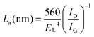
| Fig. 15 (a) H and C atom densities in C2F6/H2 VHFCCP + MW PECVD and height of the grown VG as a function of the total pressure during the formation of VG at a microwave power of 250 W and a VHF power of 270 W. (b–d) SEM images of VG grown by pressures of 13.3, 53.3, and 80.0 Pa, respectively. (e) Raman spectra of VG grown at 13.3, 53.3, and 80.0 Pa. Information on plasma type and growth conditions can be found in Table 1. Reprinted with permission from ref. 84. Copyright 2009 American Institute of Physics. | ||
5 Pressure
Another important parameter significantly influencing the plasma properties and growth process is the pressure. As briefly mentioned in Section 2.3, the dependency of gaseous ionization over pressure is described by Paschen's law.105,126 Qualitatively, Paschen's curve predicts that the breakdown voltage decreases as the product of electrode gap d and gas pressure p decreases. However, at some critical pd value, the breakdown voltage reaches a minimum, and then increases at successively smaller pd values. This is due to the fact that the mean free path of the electrons is inversely proportional to the pressure. So at a lower pressure, the mean free path of electrons can exceed the dimensions of the plasma system, and more energy is required to overcome the rapid loss of electrons to surfaces.103,127Although a minimum voltage is usually desirable for plasma treatment, most PECVD processes are conducted at a pd value smaller than the critical value. For any given PECVD system, d is usually fixed, which means that the pressure has to be lower than the critical pressure value. As mentioned previously, the lower pressure helps to achieve a higher electron temperature between two successive collisions due to the increase of the mean free path, and subsequently increase the ionization rate and maintain the stability of the plasma. However, a low pressure also means a low growth rate, while a higher plasma pressure allows a larger volume of feedstock gas input, which could possibly realize the massive production of VG at a relatively high growth rate. Bo et al. demonstrated the synthesis of VG at atmospheric pressure by using a negative normal glow discharge.34 The atmospheric growth was realized due to the extremely high local electric field near the pin tip and the external heating of the feedstock gas by a furnace. Taking advantage of the high gas flow rate at an elevated pressure, the VG growth rate could reach as high as ∼300 nm min−1 in lateral size in the first 3 min, while the thickness of the individual VG sheet (less than 10 layers of graphene) was maintained as smaller than 10 nm.
The growth rate was not simply proportional to the pressure or the gas flow rate. It is a more complex plasma chemistry process in which the pressure influences the plasma energy and the formation of active species as well. Takeuchi et al. conducted research on the influence of operating pressure on the H and C atom densities in a C2F6/H2 VHFCCP + MW PECVD system, as well as the morphology and structure of the as-grown VG.84 As shown in Fig. 15a, with an increase of pressure from 13.3 to 80 Pa, the H density increases while the C density almost remains a constant. We try to explain this observation as follows. In the current VHFCCP + MW hybrid PECVD system, H and C atoms were produced from the dissociation reactions of H2 and C2F6 in a 250 W MW reactor and a 270 W VHFCCP reactor, respectively. For a fixed reactor volume, the as-obtained H and C densities were simultaneously determined by the electron number, electron energy, and reactant molecule number. With the increasing pressure of a reactor and fixed volume, the molecule number of the gaseous precursor increased while the electron energy decreased due the reduction in the electron mean free path. For H atom formation in a high-intensity MW plasma, the plasma energy was sufficient to disassociate the increasing H2 molecules even though the electron energy was lowered, which consequently led to the increase of the H atom number. On the other hand, the C atom formation in the VHFCCP system with a relatively lower intensity was not only dominated by the increasing gaseous molecule number; the decreasing limited plasma energy was not capable of dissociating the increasing C2F6 molecules, and thus the C atom formation showed an almost ‘saturated’ state. The increasing H atoms, induced by the increasing pressure, further influenced the morphology and structure of the as-grown VG, leading to larger interlayer spacing but lower VG height, as shown in Fig. 15b–d.
6 Substrate
Initially, substrates were sputter-coated with transition metals as catalysts and the growth of VG was typically carried out in a TE-MW system.128 Later studies demonstrated that VG growth could be realized in catalyst-free systems on arbitrary substrates that can withstand a certain heating temperature, including metals, semiconductors and insulators (Cu,26,78 Ni,24,52,64,82 Au,41,52 Al,46 W,46,129 Mo,46 Zr,46 Ti,46 Hf,46 Nb,46 Ta,46 Si,23,25,29,33,36,38,46,57,58,69,81,82,84,86,108,109,111 Cr,46 stainless steel,46,64,129 carbon particle,37 crystal,88 GaAs,78 quartz,20 SiO2,23,46,52 and Al2O3 (sapphire),23,46,78etc.). Until now, successful VG growth was demonstrated on convenient planar substrates, cylinder substrates, and CNT substrates. Pattern growth on selective areas was realized as well for possible nanoelectronic applications.6.1 Pretreatment
A routine pretreatment on the growth substrate is ultrasonic cleaning in acetone or ethanol. Subsequent treatments could include the removal of the native oxide layer by hydrofluoric acid solution and rinsing with de-ionized water.33,109 Teii et al. suggested that VG growth was rather spontaneous and limited by the gas-phase conditions but not the surface conditions, different with that of diamond growth.33 However, the substrate material can affect the binding strength between the VG and the substrate; practical applications usually call for the robust growth of VG on a substrate. Generally, VG grown on carbide-forming materials could provide stronger adhesion to the substrate.87 It has been demonstrated that the stainless steel substrate showed better VG binding strength than the tungsten counterpart, according to Bo et al.'s bath sonication treatment experiments.129 As shown in Fig. 16, VG sheets were strongly connected to the stainless steel surface via a carbon layer. | ||
| Fig. 16 HRTEM image of the joint between VG and stainless steel wire. Reprinted with permission from ref. 49. Copyright 2011 Royal Society of Chemistry. | ||
Only some systems employing parallel-plate dc plasma need a particular pretreatment on the substrate to enhance VG growth. In Krivchenko et al.'s dc glow PECVD growth of VG process, the substrate surface was pretreated by a RF/MW plasma or scratched by a diamond powder.60,87 The purpose of the above pretreatment was to ensure a higher nucleation density, decreased nucleation time, and improved adhesion.
6.2 Pattern growth
Selective growth in a well-defined configuration could favor the building of integrated devices and systems for nanoelectronic applications. For example, Tyler et al. demonstrated the pattern deposition of VG on the buried cathode lines of a back-gated milliampere-class field emission device, by the growth of VG on the entire area including both the background oxidized silicon wafer and the cathode lines followed by the etching of VG at unwanted areas, to make sure that VG remained only in the centers of the cathode lines, benefiting the field emission performance.52 Other practices of pattern growth were commonly conducted with the pretreatment of growth substrates. Although Rao et al. suggested that there was no preference for a particular substrate from the viewpoint of its growth,81 growth enhancement was observed on thin layers or nanoparticles of Ti, Co, Pt, and Fe.130 This thus provides an alternative for pattern-growth of VG by depositing patterned catalyst layers on the normal substrate. For example, the VG grown on the Ti film was found to be 1.6 times higher than that on the Si substrate for the same growth conditions.130 Wu et al. also reported pattern-growth by separating the substrate using deep trenches.128 Another alternative for VG pattern-growth is through controlling the electric field on the selected substrate area. Yu et al. reported that patterned growth of VG nanosheets could be achieved through strategically patterning gold electrodes on the SiO2 surface by a normal glow dc PECVD system.41 As the first step, the growth substrate (SiO2 wafer) was patterned as a network of squares and by the letters U, W, and M, and then sputter-coated with gold electrodes of 1–5 μm width. During the VG growth, the gold network including the squares and letters U and M was grounded, whereas the letter W was floating. Modeling results of the electric field at 50 nm above the substrate indicated that the electric field above the grounded gold stripe was much larger than that above the isolated gold stripe, and the electric field above the SiO2 was the lowest, as shown in Fig. 17a–c. This configuration and electrical design would result in an electric field difference on different parts of the substrate, and further induce non-uniform ion flux distribution and finally the difference in growth rate. As shown in Fig. 17d–g, with 2 min growth, VG was synthesized on the grounded square network and the letters U and M, while there was no VG obtained on the isolated letter W. Further growth with longer duration would lead to the formation of VG on the isolated letter W, but with a lower VG height. Bo et al. reported the dependence of VG morphology and structure on the local current density for the atmospheric dc normal glow discharge PECVD process.34 Through controlling the growth time, it is possible to realize pattern-growth of VG with designed morphology and structure on the selected area. | ||
| Fig. 17 Modeling results of the electric field at 50 nm above the growth substrate with (a) a single grounded gold stripe (b) a grounded gold stripe and an isolated gold stripe, and (c) two grounded gold stripes and an isolated gold stripe. SEM images of patterned VG: (d) an overview of the VG distribution on the patterned substrate with a grounded gold square network and the letters U and M; (e) a close view showing VG growth on the grounded network and the letter U; (f and g) a close view showing VG growth on letters M and U; (h) enlarged view of VG showing vertical orientation of graphene nanosheets with a lateral dimension larger than 1 μm; (i) no VG growth was found on the isolated letter W. Reprinted with permission from ref. 41. Copyright 2011 American Chemical Society. | ||
6.3 Cylindrical substrate
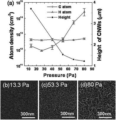
Most PECVD reactors were used for the synthesis of VG sheets on planar substrates, while some practical applications call for the growth of nanostructures on non-planar (e.g., cylindrical) surfaces. Bo et al. proposed a new reactor design for continuous synthesis of VG sheets on cylindrical wire substrates using a modified atmospheric dc normal glow PECVD system.129 Different from the previous practice where a planar substrate was fixed and mounted in a furnace, the newly designed PECVD process was conducted in a four-way quartz cross-tube outside the furnace to enable the free rotation/movement of the cylindrical growth substrates. A U-shaped reactor was used to provide additional residence time for the feed gases inside the furnace and thus enhance the heat transfer. During the VG growth, the simultaneous rotation and axial movement of the cylindrical substrate in a controlled fashion (i.e., the so-called ‘dynamic mode’ synthesis) led to the uniform growth of VG. As shown in Fig. 15a, after 3 min synthesis, the length of the VG growth region could reach ∼30 mm, including a uniform growth region of about 20 mm. Moreover, in the uniform growth region, VG morphology showed excellent uniformity in both the circumferential and the axial directions, as shown in Fig. 18b–d, which are the SEM images of the deposits at three different locations on the wire surface. The above VG growth on a cylindrical substrate could benefit the immediate application of VG coated metallic wires, such as the nanosized corona discharge plasma for indoor electrostatic devices.49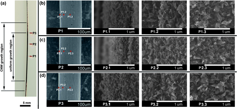 | ||
| Fig. 18 (a) Optical image of the stainless steel wire after 3 min ‘dynamic mode’ VG synthesis in a modified dc normal glow PECVD system; (b–d) SEM images of the deposits at three locations in the uniform growth region. Reprinted with permission from ref. 129. Copyright 2011 American Institute of Physics. | ||
6.4 CNT substrate
Compared with those grown on planar substrates, VG grown on CNTs could lead to the full utilization of all three of its dimensions. VG-on-CNT hierarchical nanostructure attracted certain interest since it provides a higher surface area due to the exposed graphene edges, compared with the pristine CNTs, and thus could possible benefit applications such as electrochemical electrodes, catalyst supports, and gas sensors.61,131 Two methods of producing VG-on-CNT hybrid nanostructure will be described as the following.Parker et al. reported the synthesis of graphenated carbon nanotubes (g-CNTs) in a 915 MHz MW PECVD reactor with 10 kW maximum input power.131,132 In this system, a vertically aligned CNT array was first produced and then the further in situ growth led to the formation of small foliates from the CNT sidewall. With good control of the growth conditions, g-CNTs with different VG densities were obtained, as shown in Fig. 19. High density VG sheets were synthesized on CNTs, as shown in Fig. 19c, via the secondary nucleation on the initially grown foliates. A possible growth mechanism based on the buckling of CNTs with longer growth duration was proposed. This method of growing g-CNTs required a relatively large diameter of CNTs to ensure an easy buckling, benefiting the formation of foliate nucleation site and strain relaxation of external CNT walls; the smallest diameter CNTs exhibiting graphitic foliates in this work was reported as 80 nm.
 | ||
| Fig. 19 SEM images of graphenated carbon nanotubes (g-CNTs): (a) low-density graphene foliates on a CNT, (b) medium-density graphene foliates on a CNT, (c) high-density graphene foliates on a CNT. Reprinted with permission from ref. 131. Copyright 2012 Springer. | ||
Yu et al. conducted VG growth on both the horizontally dispersed and vertically aligned CNTs by an atmospheric dc normal glow discharge PECVD system.61 For this method, there was almost no requirement on the CNT diameter, where VG nanosheets were successfully grown on CNTs of ∼15 nm in diameter. With a 1 min PECVD process, CNT–graphene hybrid structures were obtained with graphene sheets (<10 nm thick) spreading off the host CNTs (Fig. 20a and b), in contrast to the smooth surface of pristine CNTs before the graphene growth. The lateral dimension of the graphene typically ranged from 200 to 500 nm, which is consistent with a ∼300 nm min−1 growth rate previously observed with the same technique and could be controlled by the growth time and the CH4 concentration.34 By simply using a different substrate, graphene growth was also performed on vertically aligned CNTs. Graphene sheets could be grown on the entire external surface of every single vertical CNT (Fig. 20c). The inset of Fig. 20c shows that, although the CNT stem was uniform in diameter, a much larger VG corolla capped the tube tip, suggesting that the VG nanosheets grew faster on the tip portion of a vertical CNT where the local electric field is higher, leading to faster graphene growth near the CNT tip.41 Large graphene sheets with lateral dimensions of nearly 1 μm can be grown in some cases (Fig. 20d). The CNT–graphene interface has significant influence on the characteristics of the CNT–graphene hybrid structure. Fig. 20e is a representative HRTEM image that shows a few-layer graphene sheet growing directly off a host CNT; individual graphene layers can be discerned. The graphene and the host CNT are inherently bonded via sp2 carbons, evidenced by the matching lattice fringes of the graphene and those of CNTs. A noteworthy increase of the I(2D)/I(G) ratio in Raman spectra suggested the presence of more sp2 carbon domains after the graphene growth on CNTs (Fig. 20f). Compared with the method proposed by Parker et al.,131 there was no certain requirement on the CNT diameter. The fusing of VG with CNT into a single unified structure represents a giant step toward engineering interfaces between constituent components in hybrid nanostructures.
 | ||
| Fig. 20 (a) SEM image of VG-on-CNT hybrid structures. (b) TEM image of VG grown on CNTs suspended on a Cu TEM grid. (c) SEM image of VG grown on vertically aligned CNTs; the inset is a TEM image of the tip of a VG-on-CNTs, where the CNT stem (dark) is clearly distinguished from VG (bright). (d) A close view of the VG-on-CNTs tip in panel (c). (e) HRTEM image of a VG-on-CNTs structure showing that the VG is inherently bonded to the host CNT. (f) Raman spectra of pristine CNT (black) and VG-on-CNTs (red) films. Reprinted with permission from ref. 61. Copyright 2011 American Chemical Society. | ||
7 Challenge
The advantages of vertical orientation of the as-grown VG have been extensively reported. Broad VG applications call for further development of VG growth techniques to solve the following three challenges: morphology/structure controlled growth, massive production, and low-temperature growth.As mentioned in the Introduction section, the VG morphology and structure strongly influence the application performance; therefore, the growth of VG in a controlled manner is required. Better understanding of the VG growth mechanism could help provide information and guidance for controlled growth. The first is to identify the key parameter determining the growth orientation.
Different from the CVD of graphene, whose growth mechanism has been well proposed, the initial nucleation and subsequent evolution of VG are yet to be convincingly interpreted. However, previous studies on graphene may spark inspiration eventually leading to a full understanding of VG growth. Reasonably high quality graphene can be grown on transition metal substrates such as Ni,133 Pd,134 Ru,135 Ir,136 or Cu.137 The growth on relatively inexpensive polycrystalline Ni and Cu substrates has triggered particular interest in large-area deposition. However, the fundamental limitation of Ni as a catalyst is that both single and multiple layers of graphene grow simultaneously within small regions (several to tens of microns) over the entire substrate.138 This is a direct result of high carbon solubility in Ni (∼0.6 wt% at 1326 °C). The graphene nucleation on Ni is subjected to a dissolution and a subsequent out-diffusion (precipitation) process. Carbon preferentially precipitates out at the grain boundaries of polycrystalline Ni substrates so that the thickness of the graphite at the grain boundaries is larger than that within the grains. Thus, the number of graphene layers can significantly vary along the surface of Ni.139
On the other hand, the graphene growth on Cu shows a substantially different characteristic since the carbon solubility in Cu is only 0.001–0.008 wt% at 1084 °C.140,141 Thus the graphene nucleation on Cu is on the surface rather than in the bulk. The nucleation can be initiated at active sites of Cu surface, such as impurities, sharp wrinkles, and defects.142–144 CH4 dissociates and is chemically adsorbed on the Cu surface to form active carbon species (CHx).145,146 Then the carbon monomers (CHx) undergo diffusion on the Cu surface and form thermodynamically stable CnHy at the active sites of the Cu surface,146 ultimately leading to the formation of graphene nuclei. Once the graphene nuclei are formed, most of the active carbon species will be captured and consumed in the growth of graphene, reducing the probability that new graphene nuclei will be formed in the nearby areas of the Cu catalyst.142,147 Based on a recent study, the carbon–Cu interaction is weak.148 As a result, the graphene lattice shows no definite epitaxial relationship with the underlying Cu substrate, and can cross Cu grain boundaries.142
Back to the VG growth where the catalyst was commonly not a necessity, much research has been conducted focusing on its initial nucleation stage and the subsequent vertical growth. Kondo et al. suggested that the initially nucleated graphene sheets were randomly orientated; however, those standing almost vertically on the substrate grow faster due to the growth rate difference between the directions along the expanding graphene sheets and along the stacking, the preference in radical diffusion, and the overshadow effect.86 Cheng and Teii also suggested crowding effects due to the dense wall growth that would force the walls to align vertically.109 Zhang et al., attributed the formation of nucleation sites to the protruding particles formed at the substrate surface which were considered to cause accumulation of hydrocarbon ions.58 It was accepted by some groups that the graphene growth orientation underwent a change from initially parallel to perpendicular to the substrate, caused by the formation of new crystalline phases149 or the so-called Volmer–Weber mechanism.79,96 Yoshimura et al. conducted grazing incidence X-ray diffraction study on the as-grown deposits and suggested that it was the formation of a new crystalline phase (possibly a carbon allotrope) at the critical deposition time that changed the orientation of the graphene layers.149 Zhu et al. investigated the initial growth stages of VG and suggested the onset of vertical growth at grain boundaries of polycrystalline Ni substrate as a possibility.96 Malesevic et al. pointed that a base graphite layer was formed parallel to the substrate and then the growth orientation turned to be almost perpendicular to the substrate beginning with the formation of upward curling crack edges (served as the nucleation sites for vertical growth), possibly due to temperature gradients, ion bombardment and mismatch between lattice parameters of the substrate material and graphite.79 After the formation of upward curling crack edges, the further vertical growth of VG nanosheets was possibly attributed to the very high surface mobility of incoming carbon-bearing species, and the electric field perpendicular to substrate (if it exists). A VG growth model combining the effects of carbon diffusion and electric field, as shown in Fig. 21a, was proposed by Zhu et al.96 The high surface diffusion rates, caused by the large difference between the surface adsorption energy (∼0.13 eV) and the surface diffusion energy (∼1.7 eV) for a carbon atom (coming from the growth species) on the graphene surface, could help the migration of carbon atoms along the graphene surface leading to vertical growth. The estimated surface diffusion length was ∼3.7 μm for both ICP and TE-MW PECVD systems with a substrate temperature of 1000 K, which theoretically allows the vertical growth of VG to this length.58,96 Zhang et al. reported that the vertical growth length could reach 4.7 mm (with the help of a dc bias) with a 20 min growth in a TE-MW PECVD reactor (employing CH4/H2), while further growth to 60 min led to the formation of a thick layer of a-C at the interface between the VG and the substrate, which was attributed to the insufficient diffusion of carbon atoms to the top edge of VG with the increasing sheet height.58 Although it was demonstrated that VG nanosheets could be obtained using hot filament CVD where the effect of the electric field was weak,19,27,31,57,66 the introduction of a proper electric field was believed to help the alignment of VG.96,150 A dc bias of several hundreds of volts was thus employed in some TE- and TM-MW systems.58,78 Soin et al. suggested that the governing factors for non-catalytic growth of VG are plasma chemistry and the electric field.50 Wu et al. provided relevant evidence about the significant role of electric field on the formation of carbon deposits and the growth orientation of graphene layers, by introducing a substrate perpendicular to the growth substrate.13,150 Similarly, a grounded conducting metallic cylinder was vertically placed on the grounded substrate by Zhu et al., and they found the growth orientation of VG followed the local electric field direction, as shown in Fig. 21b.96
 | ||
Fig. 21 (a) Schematic illustration of VG growth model. ![[E with combining right harpoon above (vector)]](https://www.rsc.org/images/entities/i_char_0045_20d1.gif) : direction of the electric field near a substrate surface; CHx: carbon-bearing growth species impinging from the gas phase; Cg: growth species diffuse along VG surface; H: atomic hydrogen impinging from the gas phase; CHy: defects removed from VG by atomic hydrogen etching effect. (b) SEM image of aligned VG on Si substrate formed around a grounded metal electrode. The direction of the nanosheet alignment is along the radial direction of the round electrode. Reprinted with permission from ref. 96. Copyright 2007 Elsevier. : direction of the electric field near a substrate surface; CHx: carbon-bearing growth species impinging from the gas phase; Cg: growth species diffuse along VG surface; H: atomic hydrogen impinging from the gas phase; CHy: defects removed from VG by atomic hydrogen etching effect. (b) SEM image of aligned VG on Si substrate formed around a grounded metal electrode. The direction of the nanosheet alignment is along the radial direction of the round electrode. Reprinted with permission from ref. 96. Copyright 2007 Elsevier. | ||
Another important issue is the careful selection of growth precursors and the feed gas proportion. VG nanosheets grown with using CH4/N2 (ref. 50) or CH4/H2 (ref. 83) precursors were observed using XPS to have ∼4.5% (ref. 50) or 5% (ref. 83) oxygen. This small amount of oxygen was considered to be related to sample exposure to the ambient environment,50 and it was unable to be removed by a dc hydrogen plasma treatment at 700 °C although the surface could become rough and the surface-to-volume ratio could be enlarged.83 When H2O was introduced into the growth system, VG nanosheets contained 71.1% non-oxygenated ring C, 18.5% sp3 C hybridized to C (C–C), 9.1% C in C–OH bonds, 1.1% carboxylate carbon (OC–OH), and <0.2% carbonyl carbon. After a thermal annealing in H2 for 2 h at 900 °C, only a small fraction of C in C–OH of 1.7% remained in the VG nanosheets and C in CC and C–C bonds increased to 72.8% and 25.5%, respectively. Furthermore, it is crucial to select a proper a-C etchant for a certain plasma source and control well its ratio in the feedstock gases aiming at high quality growth (e.g., crystalline graphitic structure and the sharp edges). Although the a-C etchant sources for different plasma sources could be different, most a-C etchant will simultaneously etch a-C, sp2 and sp3 hybridized carbon. Typically, the OH radicals will help to etch a-C while an overload of OH radicals will destroy the as-grown VG nanosheets.34
Meanwhile, growth of VG at a high growth rate on large areas remains a critical prerequisite for industrial applications. Compared with graphene prepared by chemical method, i.e., synthesis of graphene oxide (GO) by the modified Hummer's method and the subsequent reduction of GO,151 PECVD synthesis can result in the orientated growth of graphene nanosheets with non-agglomerated morphology; however, its disadvantages include a low yield and a relatively low growth rate, which are potential inherent drawbacks of PECVD techniques (not only for the growth of VG). It should be noted that an important factor leading to these disadvantages is the operating pressure. As mentioned in Section 5, the feedstock gas flow rate and plasma energy are two competing factors: most PECVD processes are conducted at a low pressure to achieve a relatively long mean free path of electrons while the massive production of VG calls for a large volume of gas input. From this point of view, the atmospheric growth with elevated plasma energy could be used to solve this problem.
Finally, the growth of high-quality VG at a lower temperature would make it more practical in many aspects. For example, fabrication of VG on high-performance display glass needs a growth temperature lower than 660 °C.152 Furthermore, VG would become compatible with flexible substrates (e.g., plastics) by further lowering the temperature, opening new applications of VG in the area of flexible electronic devices.153
8 Conclusions
PECVD employing a variety of plasma sources such as MW, RF, and dc discharges with different reactor configurations has been successfully demonstrated for VG growth. The VG growth can be realized not only on the full- or selected-area of convenient planar substrates, but also on cylindrical and CNT substrates. While extensive studies have been conducted to reveal the influence of various key parameters, such as feedstock gas type and proportion, temperature and pressure, electric field and localized current density, on plasma behavior and VG growth performance, it is still a challenge to build a unified theory to unveil the growth mechanism (e.g., the detailed growth process, key species influencing VG morphology and structure, and the critical factor to aligned growth, etc.), and to provide guidance for optimum growth conditions (e.g., the selection of a-C etchants, the proper gas proportion, and the optimized growth temperature and pressure for specific applications) for different plasma sources. Further understanding of several key issues on controlled VG growth and plasma chemistry is warranted for fast, large-scale production of high quality VG and its successful applications.Acknowledgements
The authors acknowledge the financial support from the National Basic Research Program of China (973 Program, no. 2011CB201500). Z. Bo acknowledges the Foundation of National Excellent Doctoral Dissertation of China (no. 201238), the Important Project on Science and Technology of Zhejiang Province (no. 2008C13024-1), the Specialized Research Fund for the Doctoral Program of Higher Education (no. 20120101120140), and the Qianjiang Talent Project of Zhejiang Province (no. 2012R10028). J. Chen acknowledges the financial support from the National Science Foundation (no. CMMI-0900509), and the Department of Energy (no. DE-EE-0003208).Notes and references
- A. V. Melechko, V. I. Merkulov, T. E. McKnight, M. A. Guillorn, K. L. Klein, D. H. Lowndes and M. L. Simpson, J. Appl. Phys., 2005, 97, 041301 CrossRef.
- X. D. Wang, C. J. Summers and Z. L. Wang, Nano Lett., 2004, 4, 423–426 CrossRef CAS.
- D. Whang, S. Jin, Y. Wu and C. M. Lieber, Nano Lett., 2003, 3, 1255–1259 CrossRef CAS.
- P. M. Ajayan, O. Stephan, C. Colliex and D. Trauth, Science, 1994, 265, 1212–1214 CAS.
- W. Z. Li, S. S. Xie, L. X. Qian, B. H. Chang, B. S. Zou, W. Y. Zhou, R. A. Zhao and G. Wang, Science, 1996, 274, 1701–1703 CrossRef CAS.
- S. S. Fan, M. G. Chapline, N. R. Franklin, T. W. Tombler, A. M. Cassell and H. J. Dai, Science, 1999, 283, 512–514 CrossRef CAS.
- R. H. Baughman, C. X. Cui, A. A. Zakhidov, Z. Iqbal, J. N. Barisci, G. M. Spinks, G. G. Wallace, A. Mazzoldi, D. De Rossi, A. G. Rinzler, O. Jaschinski, S. Roth and M. Kertesz, Science, 1999, 284, 1340–1344 CrossRef CAS.
- C. V. Nguyen, L. Delzeit, A. M. Cassell, J. Li, J. Han and M. Meyyappan, Nano Lett., 2002, 2, 1079–1081 CrossRef CAS.
- I. Janowska, G. Wine, M. J. Ledoux and C. Pham-Huu, J. Mol. Catal. A: Chem., 2007, 267, 92–97 CrossRef CAS.
- I. Janowska, S. Hajiesmaili, D. Begin, V. Keller, N. Keller, M.-J. Ledoux and C. Pham-Huu, Catal. Today, 2009, 145, 76–84 CrossRef CAS.
- K. S. Novoselov, A. K. Geim, S. V. Morozov, D. Jiang, Y. Zhang, S. V. Dubonos, I. V. Grigorieva and A. A. Firsov, Science, 2004, 306, 666–669 CrossRef CAS.
- K. S. Novoselov, A. K. Geim, S. V. Morozov, D. Jiang, M. I. Katsnelson, I. V. Grigorieva, S. V. Dubonos and A. A. Firsov, Nature, 2005, 438, 197–200 CrossRef CAS.
- Y. H. Wu, B. J. Yang, B. Y. Zong, H. Sun, Z. X. Shen and Y. P. Feng, J. Mater. Chem., 2004, 14, 469–477 RSC.
- E. Luais, M. Boujtita, A. Gohier, A. Tailleur, S. Casimirius, M. A. Djouadi, A. Granier and P. Y. Tessier, J. Appl. Phys., 2009, 95, 014104 Search PubMed.
- S. C. Shin, A. Yoshimura, T. Matsuo, M. Mori, M. Tanimura, A. Ishihara, K.-i. Ota and M. Tachibana, J. Appl. Phys., 2011, 110, 104308 CrossRef.
- H. G. Jain, H. Karacuban, D. Krix, H. W. Becker, H. Nienhaus and V. Buck, Carbon, 2011, 49, 4987–4995 CrossRef CAS.
- A. Malesevic, S. Vizireanu, R. Kemps, A. Vanhulsel, C. Van Haesendonck and G. Dinescu, Carbon, 2007, 45, 2932–2937 CrossRef CAS.
- T. Dikonimos, L. Giorgi, R. Giorgi, N. Lisi, E. Salernitano and R. Rossi, Diamond Relat. Mater., 2007, 16, 1240–1243 CrossRef CAS.
- S. Shimabukuro, Y. Hatakeyama, M. Takeuchi, T. Itoh and S. Nonomura, Thin Solid Films, 2008, 516, 710–713 CrossRef CAS.
- W. Takeuchi, M. Ura, M. Hiramatsu, Y. Tokuda, H. Kano and M. Hori, Appl. Phys. Lett., 2008, 92, 213103 CrossRef.
- B. J. Yang, Y. H. Wu, B. Y. Zong and Z. X. Shen, Nano Lett., 2002, 2, 751–754 CrossRef CAS.
- T. Mori, M. Hiramatsu, K. Yamakawa, K. Takeda and M. Hori, Diamond Relat. Mater., 2008, 17, 1513–1517 CrossRef CAS.
- M. Hiramatsu, K. Shiji, H. Amano and M. Hori, Appl. Phys. Lett., 2004, 84, 4708–4710 CrossRef CAS.
- G. Sato, T. Morio, T. Kato and R. Hatakeyama, Jpn. J. Appl. Phys., 2006, 45, 5210–5212 CrossRef CAS.
- A. T. H. Chuang, B. O. Boskovic and J. Robertson, Diamond Relat. Mater., 2006, 15, 1103–1106 CrossRef CAS.
- K. Yu, Z. Bo, G. Lu, S. Mao, S. Cui, Y. Zhu, X. Chen, R. S. Ruoff and J. Chen, Nanoscale Res. Lett., 2011, 6, 202 CrossRef.
- P. A. Eslami, M. Ghoranneviss, S. Moradi, P. A. Azar, S. A. Khorrami and S. N. Laheghi, Fullerenes, Nanotubes, Carbon Nanostruct., 2011, 19, 237–249 CrossRef CAS.
- C. X. Zhang, J. Hu, X. K. Wang, X. D. Zhang, H. Toyoda, M. Nagatsu and Y. D. Meng, Carbon, 2012, 50, 3731–3738 CrossRef CAS.
- S. Kondo, M. Hori, K. Yamakawa, S. Den, H. Kano and M. Hiramatsu, J. Vac. Sci. Technol., B: Microelectron. Nanometer Struct.–Process., Meas., Phenom., 2008, 26, 1294–1300 CrossRef CAS.
- S. Shimada, K. Teii and M. Nakashima, Diamond Relat. Mater., 2010, 19, 956–959 CrossRef CAS.
- S. Shimabukuro, Y. Hatakeyama, M. Takeuchi, T. Itoh and S. Nonomura, Jpn. J. Appl. Phys., 2008, 47, 8635–8640 CrossRef CAS.
- P. Hojati-Talemi and G. P. Simon, Carbon, 2010, 48, 3993–4000 CrossRef CAS.
- K. Teii, S. Shimada, M. Nakashima and A. T. H. Chuang, J. Appl. Phys., 2009, 106, 084303 CrossRef.
- Z. Bo, K. H. Yu, G. H. Lu, P. X. Wang, S. Mao and J. H. Chen, Carbon, 2011, 49, 1849–1858 CrossRef CAS.
- X. Zhao, H. Tian, M. Zhu, K. Tian, J. J. Wang, F. Kang and R. A. Outlaw, J. Power Sources, 2009, 194, 1208–1212 CrossRef CAS.
- Z. P. Wang, M. Shoji and H. Ogata, Appl. Surf. Sci., 2011, 257, 9082–9085 CrossRef CAS.
- J. N. Tiwari, R. N. Tiwari, G. Singh and K. L. Lin, Plasmonics, 2010, 6, 67–73 CrossRef.
- M. Y. Zhu, R. A. Outlaw, M. Bagge-Hansen, H. J. Chen and D. M. Manos, Carbon, 2011, 49, 2526–2531 CrossRef CAS.
- M. Y. Chen, C. M. Yeh, J. S. Syu, J. Hwang and C. S. Kou, Nanotechnology, 2007, 18, 185706 CrossRef.
- S. Wang, J. Wang, P. Miraldo, M. Zhu, R. Outlaw, K. Hou, X. Zhao, B. C. Holloway, D. Manos, T. Tyler, O. Shenderova, M. Ray, J. Dalton and G. McGuire, Appl. Phys. Lett., 2006, 89, 183103 CrossRef.
- K. H. Yu, P. X. Wang, G. H. Lu, K. H. Chen, Z. Bo and J. H. Chen, J. Phys. Chem. Lett., 2011, 2, 537–542 CrossRef CAS.
- H. Kim, Z. Wen, K. Yu, O. Mao and J. Chen, J. Mater. Chem., 2012, 22, 15514–15518 RSC.
- N. G. Shang, P. Papakonstantinou, M. McMullan, M. Chu, A. Stamboulis, A. Potenza, S. S. Dhesi and H. Marchetto, Adv. Funct. Mater., 2008, 18, 3506–3514 CrossRef CAS.
- W. C. Shih, J. M. Jeng, C. T. Huang and J. T. Lo, Vacuum, 2010, 84, 1452–1456 CrossRef CAS.
- T. C. Hung, C. F. Chen and W. T. Whang, Electrochem. Solid-State Lett., 2009, 12, K41–K44 CrossRef CAS.
- J. J. Wang, M. Y. Zhu, R. A. Outlaw, X. Zhao, D. M. Manos, B. C. Holloway and V. P. Mammana, Appl. Phys. Lett., 2004, 85, 1265–1267 CrossRef CAS.
- O. Tanaike, N. Kitada, H. Yoshimura, H. Hatori, K. Kojima and M. Tachibana, Solid State Ionics, 2009, 180, 381–385 CrossRef CAS.
- A. Sharma, T. Kyotani and A. Tomita, Carbon, 2000, 38, 1977–1984 CrossRef CAS.
- Z. Bo, K. Yu, G. Lu, S. Cui, S. Mao and J. Chen, Energy Environ. Sci., 2011, 4, 2525–2528 CAS.
- N. Soin, S. S. Roy, T. H. Lim and J. A. D. McLaughlin, Mater. Chem. Phys., 2011, 129, 1051–1057 CrossRef CAS.
- K. Hou, R. A. Outlaw, S. Wang, M. Y. Zhu, R. A. Quinlan, D. M. Manos, M. E. Kordesch, U. Arp and B. C. Holloway, Appl. Phys. Lett., 2008, 92, 133112 CrossRef.
- T. Tyler, O. Shenderova, M. Ray, J. Dalton, J. Wang, R. Outlaw, M. Zhu, X. Zhao, G. McGuire and B. C. Holloway, J. Vac. Sci. Technol., B: Microelectron. Nanometer Struct.–Process., Meas., Phenom., 2006, 24, 2295–2301 CrossRef CAS.
- W. C. Shih, J. M. Jeng, J. T. Lo, H. C. Chen and I. N. Lin, J. Mater. Sci.: Mater. Electron., 2009, 21, 926–931 CrossRef.
- W. Takeuchi, H. Kondo, T. Obayashi, M. Hiramatsu and M. Hori, Appl. Phys. Lett., 2011, 98, 123107 CrossRef.
- D. Banerjee, S. Mukherjee and K. K. Chattopadhyay, Appl. Surf. Sci., 2011, 257, 3717–3722 CrossRef CAS.
- N. Jiang, H. X. Wang, H. Sasaoka, T. Deno and K. Nishimura, Mater. Lett., 2010, 64, 2025–2027 CrossRef CAS.
- N. G. Shang, F. C. K. Au, X. M. Meng, C. S. Lee, I. Bello and S. T. Lee, Chem. Phys. Lett., 2002, 358, 187–191 CrossRef CAS.
- Y. Zhang, J. Du, S. Tang, P. Liu, S. Deng, J. Chen and N. Xu, Nanotechnology, 2012, 23, 015202 CrossRef.
- J. H. Deng, R. T. Zheng, Y. Zhao and G. A. Cheng, ACS Nano, 2012, 6, 3727–3733 CrossRef CAS.
- V. A. Krivchenko, A. A. Pilevsky, A. T. Rakhimov, B. V. Seleznev, N. V. Suetin, M. A. Timofeyev, A. V. Bespalov and O. L. Golikova, J. Appl. Phys., 2010, 107, 014315 CrossRef.
- K. H. Yu, G. H. Lu, Z. Bo, S. Mao and J. H. Chen, J. Phys. Chem. Lett., 2011, 2, 1556–1562 CrossRef CAS.
- M. Cai, R. A. Outlaw, S. M. Butler and J. R. Miller, Carbon, 2012, 50, 5481–5488 CrossRef CAS.
- J. R. Miller, R. A. Outlaw and B. C. Holloway, Science, 2010, 329, 1637–1639 CrossRef CAS.
- Z. Bo, Z. Wen, H. Kim, G. Lu, K. Yu and J. Chen, Carbon, 2012, 50, 4379–4387 CrossRef CAS.
- X. C. Xiao, P. Liu, J. S. Wang, M. W. Verbrugge and M. P. Balogh, Electrochem. Commun., 2011, 13, 209–212 CrossRef CAS.
- L. Giorgi, T. D. Makris, R. Giorgi, N. Lisi and E. Salernitano, Sens. Actuators, B, 2007, 126, 144–152 CrossRef CAS.
- Y. H. Wu, T. Yu and Z. X. Shen, J. Appl. Phys., 2010, 108, 071301 CrossRef.
- J. J. Wang, M. Y. Zhu, R. A. Outlaw, X. Zhao, D. M. Manos and B. C. Holloway, Carbon, 2004, 42, 2867–2872 CrossRef CAS.
- K. Shiji, M. Hiramatsu, A. Enomoto, N. Nakamura, H. Amano and M. Hori, Diamond Relat. Mater., 2005, 14, 831–834 CrossRef CAS.
- S. Vizireanu, S. D. Stoica, C. Luculescu, L. C. Nistor, B. Mitu and G. Dinescu, Plasma Sources Sci. Technol., 2010, 19, 034016 CrossRef.
- K. Yu, Z. Wen, H. Pu, G. Lu, Z. Bo, H. Kim, Y. Qian, E. Andrew, S. Mao and J. Chen, J. Mater. Chem. A, 2013, 1, 188–193 CAS.
- J. J. Yoo, K. Balakrishnan, J. S. Huang, V. Meunier, B. G. Sumpter, A. Srivastava, M. Conway, A. L. M. Reddy, J. Yu, R. Vajtai and P. M. Ajayan, Nano Lett., 2011, 11, 1423–1427 CrossRef CAS.
- E. Cappelli, S. Orlando, G. Mattei, C. Scilletta, F. Corticelli and P. Ascarelli, Appl. Phys. A: Mater. Sci. Process., 2004, 79, 2063–2068 CrossRef CAS.
- K. Ostrikov and S. Xu, Plasma-Aided Nanofabrication, Wiley-VCH, Weinheim, 2007 Search PubMed.
- M. S. Bell, K. B. K. Teo, R. G. Lacerda, W. I. Milne, D. B. Hash and M. Meyyappan, Pure Appl. Chem., 2006, 78, 1117–1125 CrossRef CAS.
- K. Ostrikov, Plasma Nanoscience, Wiley-VCH, Weinheim, 2008 Search PubMed.
- Y. Ando, X. Zhao and M. Ohkohchi, Carbon, 1997, 35, 153–158 CrossRef CAS.
- Y. H. Wu, P. W. Qiao, T. C. Chong and Z. X. Shen, Adv. Mater., 2002, 14, 64–67 CrossRef CAS.
- A. Malesevic, R. Vitchev, K. Schouteden, A. Volodin, L. Zhang, G. Van Tendeloo, A. Vanhulsel and C. Van Haesendonck, Nanotechnology, 2008, 19, 305604 CrossRef.
- L. Y. Zeng, D. Lei, W. B. Wang, J. Q. Liang, Z. Q. Wang, N. Yao and B. L. Zhang, Appl. Surf. Sci., 2008, 254, 1700–1704 CrossRef CAS.
- B. P. C. Rao, R. Maheswaran, S. Ramaswamy, O. Mahapatra, C. Gopalakrishanan and D. J. Thiruvadigal, Fullerenes, Nanotubes, Carbon Nanostruct., 2009, 17, 625–635 CrossRef CAS.
- A. N. Obraztsov, A. P. Volkov, K. S. Nagovitsyn, K. Nishimura, K. Morisawa, Y. Nakano and A. Hiraki, J. Phys. D: Appl. Phys., 2002, 35, 357–362 CrossRef CAS.
- N. Jiang, H. X. Wang, H. Zhang, H. Sasaoka and K. Nishimura, J. Mater. Chem., 2010, 20, 5070–5073 RSC.
- W. Takeuchi, H. Sasaki, S. Kato, S. Takashima, M. Hiramatsu and M. Hori, J. Appl. Phys., 2009, 105, 113305 CrossRef.
- M. Hiramatsu and M. Hori, International Conference of Microprocesses and Nanotechnology, 2005, pp. 248–249 Search PubMed.
- S. Kondo, S. Kawai, W. Takeuchi, K. Yamakawa, S. Den, H. Kano, M. Hiramatsu and M. Hori, J. Appl. Phys., 2009, 106, 094302 CrossRef.
- V. A. Krivchenko, V. V. Dvorkin, N. N. Dzbanovsky, M. A. Timofeyev, A. S. Stepanov, A. T. Rakhimov, N. V. Suetin, O. Y. Vilkov and L. V. Yashina, Carbon, 2012, 50, 1477–1487 CrossRef CAS.
- S. Mori, T. Ueno and M. Suzuki, Diamond Relat. Mater., 2011, 20, 1129–1132 CrossRef CAS.
- H. Chatei, M. Belmahi, M. B. Assouar, L. Le Brizoual, P. Bourson and J. Bougdira, Diamond Relat. Mater., 2006, 15, 1041–1046 CrossRef CAS.
- K. Kobashi, K. Nishimura, Y. Kawate and T. Horiuchi, Phys. Rev. B, 1988, 38, 4067–4084 CrossRef CAS.
- F. Silva, X. Bonnin, J. Scharpf and A. Pasquarelli, Diamond Relat. Mater., 2010, 19, 397–403 CrossRef CAS.
- H. Sugai, I. Ghanashev and K. Mizuno, Appl. Phys. Lett., 2000, 77, 3523–3525 CrossRef CAS.
- M. Nagatsu, G. Xu, I. Ghanashev, M. Kanoh and H. Sugai, Plasma Sources Sci. Technol., 1997, 6, 427–434 CrossRef CAS.
- P. Chabert and N. Braithwaite, Physics of Radio-Frequency Plasmas, Cambridge University Press, New York, 2011 Search PubMed.
- J. Hopwood, Plasma Sources Sci. Technol., 1992, 1, 109–116 CrossRef CAS.
- M. Y. Zhu, J. J. Wang, B. C. Holloway, R. A. Outlaw, X. Zhao, K. Hou, V. Shutthanandan and D. M. Manos, Carbon, 2007, 45, 2229–2234 CrossRef CAS.
- A. N. Obraztsov, A. A. Zolotukhin, A. O. Ustinov, A. P. Volkov, Y. Svirko and K. Jefimovs, Diamond Relat. Mater., 2003, 12, 917–920 CrossRef CAS.
- S. Kurita, A. Yoshimura, H. Kawamoto, T. Uchida, K. Kojima, M. Tachibana, P. Molina-Morales and H. Nakai, J. Appl. Phys., 2005, 97, 104320 CrossRef.
- B. M. Kostya Ostrikov, U. Cvelbar and A. B. Murphy, J. Phys. D: Appl. Phys., 2011, 44, 174001 CrossRef.
- M. Y. Zhu, J. J. Wang, R. A. Outlaw, K. Hou, D. M. Manos and B. C. Holloway, Diamond Relat. Mater., 2007, 16, 196–201 CrossRef CAS.
- A. P. Paranjpe, J. P. McVittie and S. A. Self, J. Appl. Phys., 1990, 67, 6718–6727 CrossRef CAS.
- J. Hopwood, C. R. Guarnieri, S. J. Whitehair and J. J. Cuomo, J. Vac. Sci. Technol., A, 1993, 11, 152–156 CAS.
- M. Lieberman and A. Lichtenberg, Principles of Plasma Discharges and Materials Processing, John Wiley & Sons, Inc., New Jersey, 2005 Search PubMed.
- K. K. Chattopadhyay and S. Matsumoto, Appl. Phys. Lett., 1995, 67, 3972–3974 CrossRef CAS.
- F. Paschen, Ann. Phys. Chem., 1889, 273, 69–75 Search PubMed.
- I. B. Denysenko, S. Xu, J. D. Long, P. P. Rutkevych, N. A. Azarenkov and K. Ostrikov, J. Appl. Phys., 2004, 95, 2713–2724 CrossRef CAS.
- Z. H. Ni, H. M. Fan, Y. P. Feng, Z. X. Shen, B. J. Yang and Y. H. Wu, J. Chem. Phys., 2006, 124, 204703 CrossRef CAS.
- N. Soin, S. S. Roy, C. O'Kane, J. A. D. McLaughlin, T. H. Lim and C. J. D. Hetherington, CrystEngComm, 2011, 13, 312–318 RSC.
- C. Y. Cheng and K. Teii, IEEE Trans. Plasma Sci., 2012, 40, 1783–1788 CrossRef CAS.
- L. G. Cancado, K. Takai, T. Enoki, M. Endo, Y. A. Kim, H. Mizusaki, A. Jorio, L. N. Coelho, R. Magalhaes-Paniago and M. A. Pimenta, Appl. Phys. Lett., 2006, 88, 163106 CrossRef.
- K. Teii and T. Ikeda, Appl. Phys. Lett., 2007, 90, 111504 CrossRef.
- B. L. French, J. J. Wang, M. Y. Zhu and B. C. Holloway, J. Appl. Phys., 2005, 97, 114317 CrossRef.
- D. M. Gruen, Annu. Rev. Mater. Sci., 1999, 29, 211–259 CrossRef CAS.
- M. Hiramatsu, K. Kato, C. H. Lau, J. S. Foord and M. Hori, Diamond Relat. Mater., 2003, 12, 365–368 CrossRef CAS.
- A. N. Goyette, Y. Matsuda, L. W. Anderson and J. E. Lawler, J. Vac. Sci. Technol., A, 1998, 16, 337–340 CAS.
- T. Shiomi, H. Nagai, K. Kato, M. Hiramatsu and M. Nawata, Diamond Relat. Mater., 2001, 10, 388–392 CrossRef CAS.
- W. Zhu, A. Inspektor, A. R. Badzian, T. McKenna and R. Messier, J. Appl. Phys., 1990, 68, 1489–1496 CrossRef CAS.
- M. Hori, H. Kondo and M. Hiramatsu, J. Phys. D: Appl. Phys., 2011, 44, 174027 CrossRef.
- C. Yamabe, S. J. Buckman and A. V. Phelps, Phys. Rev. A: At., Mol., Opt. Phys., 1983, 27, 1345–1352 CrossRef CAS.
- N. G. Shang, T. Staedler and X. Jiang, Appl. Phys. Lett., 2006, 89, 103112 CrossRef.
- E. G. Wang, Z. G. Guo, J. Ma, M. M. Zhou, Y. K. Pu, S. Liu, G. Y. Zhang and D. Y. Zhong, Carbon, 2003, 41, 1827–1831 CrossRef CAS.
- T. Vandevelde, T. D. Wu, C. Quaeyhaegens, J. Vlekken, M. D'Olieslaeger and L. Stals, Thin Solid Films, 1999, 340, 159–163 CrossRef CAS.
- H. Kersten, H. Deutsch, H. Steffen, G. M. W. Kroesen and R. Hippler, Vacuum, 2001, 63, 385–431 CrossRef CAS.
- A. Fridman and L. Kennedy, Plasma Physics and Engineering, Taylor & Francis, New York, 2006 Search PubMed.
- V. Krivchenko, P. Shevnin, A. Pilevsky, A. Egorov, N. Suetin, V. Sen, S. Evlashin and A. Rakhimov, J. Mater. Chem., 2012, 22, 16458–16464 RSC.
- Y. Yang, H. Kim, A. Starikovskiy, A. Fridman and Y. I. Cho, Water Res., 2010, 44, 3659–3668 CrossRef CAS.
- Y. Yang, H. Kim, A. Starikovskiy, Y. I. Cho and A. Fridman, Rev. Sci. Instrum., 2011, 82, 096103 CrossRef CAS.
- Y. H. Wu, B. J. Yang, G. C. Han, B. Y. Zong, H. Q. Ni, P. Luo, T. C. Chong, T. S. Low and Z. X. Shen, Adv. Funct. Mater., 2002, 12, 489–494 CrossRef CAS.
- Z. Bo, S. M. Cui, K. H. Yu, G. H. Lu, S. Mao and J. H. Chen, Rev. Sci. Instrum., 2011, 82, 086116 CrossRef.
- M. Hiramatsu and M. Hori, Carbon Nanowalls: Synthehesis and Emerging Application, Springer, New York, 2010 Search PubMed.
- C. B. Parker, A. S. Raut, B. Brown, B. R. Stoner and J. T. Glass, J. Mater. Res., 2012, 27, 1046–1053 CrossRef CAS.
- H. Cui, O. Zhou and B. R. Stoner, J. Appl. Phys., 2000, 88, 6072–6074 CrossRef CAS.
- K. S. Kim, Y. Zhao, H. Jang, S. Y. Lee, J. M. Kim, K. S. Kim, J. H. Ahn, P. Kim, J. Y. Choi and B. H. Hong, Nature, 2009, 457, 706–710 CrossRef CAS.
- S. Y. Kwon, C. V. Ciobanu, V. Petrova, V. B. Shenoy, J. Bareno, V. Gambin, I. Petrov and S. Kodambaka, Nano Lett., 2009, 9, 3985–3990 CrossRef CAS.
- P. W. Sutter, J. I. Flege and E. A. Sutter, Nat. Mater., 2008, 7, 406–411 CrossRef CAS.
- J. Coraux, A. T. N'Diaye, C. Busse and T. Michely, Nano Lett., 2008, 8, 565–570 CrossRef CAS.
- X. Li, W. Cai, J. An, S. Kim, J. Nah, D. Yang, R. Piner, A. Velamakanni, I. Jung, E. Tutuc, S. K. Banerjee, L. Colombo and R. S. Ruoff, Science, 2009, 324, 1312–1314 CrossRef CAS.
- A. N. Obraztsov, E. A. Obraztsova, A. V. Tyurnina and A. A. Zolotukhin, Carbon, 2007, 45, 2017–2021 CrossRef CAS.
- C. Mattevi, H. Kim and M. Chhowalla, J. Mater. Chem., 2011, 21, 3324–3334 RSC.
- C. Oshima and A. Nagashima, J. Phys.: Condens. Matter, 1997, 9, 1–20 CrossRef CAS.
- G. A. Lopez and E. Mittemeijer, Scr. Mater., 2004, 51, 1–5 CrossRef CAS.
- Q. Yu, L. A. Jauregui, W. Wu, R. Colby, J. Tian, Z. Su, H. Cao, Z. Liu, D. Pandey, D. Wei, T. F. Chung, P. Peng, N. P. Guisinger, E. A. Stach, J. Bao, S.-S. Pei and Y. P. Chen, Nat. Mater., 2011, 10, 443–449 CrossRef CAS.
- H. Wang, G. Wang, P. Bao, S. Yang, W. Zhu, X. Xie and W.-J. Zhang, J. Am. Chem. Soc., 2012, 134, 3627–3630 CrossRef CAS.
- Z. Luo, Y. Lu, D. W. Singer, M. E. Berck, L. A. Somers, B. R. Goldsmith and A. T. C. Johnson, Chem. Mater., 2011, 23, 1441–1447 CrossRef CAS.
- R. G. Van Wesep, H. Chen, W. Zhu and Z. Zhang, J. Chem. Phys., 2011, 134, 171105 CrossRef.
- W. Zhang, P. Wu, Z. Li and J. Yang, J. Phys. Chem. C, 2011, 115, 17782–17787 CAS.
- Z. Yan, J. Lin, Z. Peng, Z. Sun, Y. Zhu, L. Li, C. Xiang, E. L. Samuel, C. Kittrell and J. M. Tour, ACS Nano, 2012, 6, 9110–9117 CrossRef CAS.
- H. Kim, C. Mattevi, M. R. Calvo, J. C. Oberg, L. Artiglia, S. Agnoli, C. F. Hirjibehedin, M. Chhowalla and E. Saiz, ACS Nano, 2012, 6, 3614–3623 CrossRef CAS.
- H. Yoshimura, S. Yamada, A. Yoshimura, I. Hirosawa, K. Kojima and M. Tachibana, Chem. Phys. Lett., 2009, 482, 125–128 CrossRef CAS.
- Y. H. Wu, Nano Lett., 2002, 2, 355–359 CrossRef CAS.
- S. Park, J. H. An, R. D. Piner, I. Jung, D. X. Yang, A. Velamakanni, S. T. Nguyen and R. S. Ruoff, Chem. Mater., 2008, 20, 6592–6594 CrossRef CAS.
- Z. F. Ren, Z. P. Huang, J. W. Xu, J. H. Wang, P. Bush, M. P. Siegal and P. N. Provencio, Science, 1998, 282, 1105–1107 CrossRef CAS.
- V. C. Tung, L. M. Chen, M. J. Allen, J. K. Wassei, K. Nelson, R. B. Kaner and Y. Yang, Nano Lett., 2009, 9, 1949–1955 CrossRef CAS.
| This journal is © The Royal Society of Chemistry 2013 |