 Open Access Article
 This Open Access Article is licensed under a
 Creative Commons Attribution 3.0 Unported Licence
The origin of off-resonance non-linear optical activity of a gold chiral nanomaterial†
Nadia
Abdulrahman
a,
Christopher D.
Syme
a,
Calum
Jack
a,
Affar
Karimullah
ab,
Laurence D.
Barron
a,
Nikolaj
Gadegaard
b and
Malcolm
Kadodwala
*a
aSchool of Chemistry, University of Glasgow, Joseph Black Building, Glasgow G12 8QQ, UK. E-mail: malcolm.kadodwala@glasgow.ac.uk
bDivision of Biomedical Engineering, School of Engineering, University of Glasgow, Rankine Building, Glasgow G12 8LT, UK
First published on 22nd October 2013
Abstract
We demonstrate that engineered artificial gold chiral nanostructures display significant levels of non-linear optical activity even without plasmonic enhancement. Our work suggests that although plasmonic excitation enhances the intensity of second harmonic emission it is not a prerequisite for significant non-linear (second harmonic) optical activity. It is also shown that the non-linear optical activities of both the chiral nanostructures and simple chiral molecules on surfaces have a common origin, namely pure electric dipole excitation. This is a surprising observation given the significant difference in length scales, three orders of magnitude, between the nanostructures and simple chiral molecules. Intuitively, given that the dimensions of the nanostructures are comparable to the wavelength of visible light, one would expect non-localised higher multipole excitation (e.g. electric quadrupole and magnetic dipole) to make the dominant contribution to non-linear optical activity. This study provides experimental evidence that the electric dipole origin of non-linear optical activity is a generic phenomenon which is not limited to sub-wavelength molecules and assemblies. Our work suggests that viewing non-plasmonic nanostructures as “meta-molecules” could be useful for rationally designing substrates for optimal non-linear optical activity.
Introduction
Chiral plasmonic metamaterials have provoked considerable interest due to their unique optical properties. These materials can, inter alia, provide a route to negative refraction,1 act as broad band polarisers,2 and be used for ultrasensitive detection and characterisation of biological materials.3 The non-linear optical properties, and second harmonic generation (SHG) in particular, of plasmonic nanomaterials is currently a fertile area of investigation.4 Here we present an investigation of the origins of the non-linear optical activity displayed by chiral plasmonic planar nanomaterials using non-resonant optically active (OA)-second harmonic generation (SHG). We are able to probe the microscopic origins of the optical activity of the plasmonic metamaterials by utilising non-resonant scattering conditions. From measurements on left- and right-handed nanostructured substrates as well as racemic (both left and right in equal ratio) mixtures we have been able to demonstrate optical activity for off-resonance fundamental and second harmonic (SH) wavelengths. Crucially, by being able to model the SH emission using a plane wave based formalism valid for off-resonance scattering, since localised evanescent fields are not produced, we show that optical activity displayed by the chiral plasmonic materials is predominately electric dipole in origin. This is an unexpected result given that for metamaterials consisting of nanostructures with dimensions comparable to the wavelength of light, it would be expected that non-localised higher multipole excitation would make the dominant contribution to non-linear optical activity. Electric dipole excitation is the principal contribution in non-linear optical activity from aligned molecular chiral media. Our work suggests that the paradigm of artificial molecules,5 can be extended to rationalising the origins of optical activity in nanomaterials, thereby providing a framework for the rational design of nanomaterials for optimal non-linear optical activity.Although less extensively studied than molecular systems there is growing activity in SHG measurements of planar (plasmonic) nano/metamaterials. The SHG studies of plasmonic nanomaterials reported to date4,6–17 have focussed on resonantly excited systems i.e. a plasmonic mode of the nanostructure overlaps the wavelength of the incident fundamental light. Under such resonant conditions localised high intensity evanescent EM fields are generated in the vicinity of the nanostructure surfaces, resulting in a strongly varying field distribution over the nanostructure. Valev and co-workers have imaged these localised fields, or hot spots, in SHG microscopy experiments on micron sized nanostructures.10 Resonant excitation, and the subsequent generation of hot spots, leads to enhanced SH emission when compared to an unstructured surface. However, the presence of the hot-spots also means the properties of the nanostructures, in particular the second order susceptibility (χ2), exhibit strong spatial variation over the length scale of a wavelength. Therefore, SHG emission cannot be interpreted with the formalism used for molecular materials, which assumes a homogeneous χ2. To overcome such difficulties, Kauranen and co-workers have introduced the concept of a macroscopic nonlinear response tensor (NRT), which treats the sample as a ‘black box’, with the input and output radiation fields being the important parameters.14,18,19 Clearly, the microscopic origins of the SH emission is not an intrinsic parameter to the modelling in this approach.
Since in the present study we performed SHG under a non-resonant condition, there were no strongly spatially varying fields across the nanostructures. Hence the properties of the substrates can be assumed to be homogeneous and the plane wave based formalism used to describe molecular systems is valid for the metamaterials studied, and the microscopic origins of the SHG response can be determined.20–24
Optically active second harmonic generation (OA-SHG), utilising a range of measurement methodologies, has been widely used to probe the structure, including chirality, of (bio)molecular materials,24–30 and adsorbate-induced chiral perturbations of the electronic structure of achiral metal surfaces.31–33 The non-linear optical activity displayed by chiral metamaterials has been investigated less extensively.4,6–16 The focus of these studies has primarily been to utilise OA-SHG measurements to detect the chirality of the component nanostructures, and have not focussed on the origins of the non-linear optical activity.
Unlike linear optical activity in bulk isotropic chiral media, which requires interference between electric and magnetic dipole excitation,34 linear and non-linear optical activity of chiral interfaces can originate in pure electric dipole, electric quadrupole, and magnetic dipole excitations.21–24,35,36 The relative contributions of electric dipole and higher multipole terms, magnetic dipole and electric quadrupole, to non-linear optical activity has been an area of discussion in the literature. The current consensus is that pure electric dipole excitation is the dominant contribution to non-linear optical activity of molecular systems,28 although there is an example of where higher multipole contributions are comparable to electric dipole.37 Initially the large asymmetries observed in non-linear optical activity of molecular monolayers was used as prima facie evidence for the dominant contribution of electric dipole excitation.30 Subsequently, this hypothesis was more firmly established by both experiment38–40 and theory.36
The nanostructures studied in the present work display chirality on a significantly longer length scale, hundreds of nm, than the molecular and supramolecular systems previously investigated with non-linear techniques.24–30 Since the dimensions of the nanostructures are comparable with the wavelength of the fundamental and SH light, intuitively one may expect the relative contribution of non-localised higher multipole excitations to non-linear optical activity to be increased compared to molecular/supramolecular systems. This is the question that the current study seeks to address.
Experimental
We performed measurements on planar chiral nanostructured continuous films which were produced using electron beam lithography. The left-handed, right-handed and racemic nanofilms were fabricated in a two-step process. Firstly, gammadian structures of length 400 nm and thickness 130 nm (plus a 5 nm Ti adhesion layer) were fabricated on a native oxide covered silicon substrate and arranged in a square lattice with a periodicity of 800 nm. The substrates consisted of alternate 320 × 320 μm squares of nanostructures and bare substrate arranged in a checker board pattern to cover a total area of 4.8 × 4.8 mm. Subsequently, these structures were covered with a 60 nm thick Au film. SEM images of the left, right and racemic structures are shown in Fig. 1.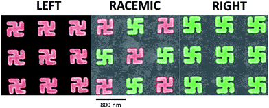 | ||
| Fig. 1 SEM images of the left (red), right (green) and racemic substrates collected post laser irradiation. | ||
To investigate the origin of the SHG we used a method previously applied to chiral molecular layers.24–30 This involves measuring the dependence of the s- or p-polarised components of the SH emission on the orientation of the linearly polarised incident light with respect to the scattering plane (denoted by the angle θ). The OA-SHG measurements were performed using a system described in detail elsewhere31–33,41 and which utilises a Nd:YAG pulsed laser (Quanta Ray Coherent Ltd) (8 ns, 1064 nm). The light was incident at the sample at an angle of 60° to the surface normal (see ESI†). Neither the fundamental (1064 nm) nor the SH (532 nm) wavelengths were resonant with any plasmonic mode of the nanomaterials (see ESI†). This was verified by extinction spectra collected from the substrates. The data were collected using energy densities of 5.3 mJ cm−2 over an area of ∼1 cm2. That this was insufficient to cause damage to the nanomaterials was confirmed by SEM measurements post laser irradiation (Fig. 1).
Theory
The electric dipole and higher multipole contributions to the SHG signal can be analysed through angle dependent measurements to yield the origin of the SHG emission,23,35,37,42,43 which enables the amplitude of the SH electric field observed in a (OA-)SHG measurement to be expressed as| Ei(2ω) = fiEp2(ω) + giEs2(ω) + hiEp(ω)Es(ω), | (1) |
The electric quadrupole and magnetic dipole elements cannot be distinguished based solely on symmetry properties. Consequently, for the type of OA-SHG measurement we have performed they are generally considered as a combined single higher multipole term.40 Kauranen et al.43 have reformulated fi, gi and hi (where i = s, p) to separate out the electric dipole (ED) and combined magnetic dipole and electric quadrupole (MD/EQ) terms:
| fp = fMD/EQp + fEDp | (2a) |
| gp = gMD/EQp + gEDp | (2b) |
| hp = hMD/EQp + hEDp | (2c) |
| fs = fMD/EQs + fEDs | (2d) |
| gs = gMD/EQs | (2e) |
| hs = hMD/EQs + hEDs | (2f) |
The multipole terms for fi, gi and hi have magnetic dipole and electric quadrupole tensor elements in common. Based on the symmetry properties of the tensor elements that constitute fMD/EQi, fEDi, gMD/EQi, gEDi, hMD/EQi and hEDi, the coefficients fs, gs and hp are only non-zero for chiral interfaces and reverse sign on changing the handedness of the surfaces. It is important to note that in contrast to the other terms, gs only depends on a multipole contribution. As will be seen later, the observation of a zero value for gs is the basis of our assignment of an electric dipole mechanism.
Since Ep = E![[thin space (1/6-em)]](https://www.rsc.org/images/entities/char_2009.gif) cosθ and Es = Esinθ, where E is the intensity of the incident field and θ is the angle of the electric field vector with respect to the scattering plane, the dependence of SH emission for a particular SH polarisation (i = s or p) is
cosθ and Es = Esinθ, where E is the intensity of the incident field and θ is the angle of the electric field vector with respect to the scattering plane, the dependence of SH emission for a particular SH polarisation (i = s or p) is
| Ii(2ω) = E4(ω)[|fi|2cos4θ + |gi|2sin4θ + (hig*i + h*igi)sin3θ cosθ + (hif*i + h*ifi)sinθ cos3θ + (fig*i + f*igi + |hi|2)sin2θ cos2θ] | (3) |
Eqn (3) can be simplified by defining real coefficients,
| αi = E4(ω)|fi|2, | (4) |
| βi = E4(ω)(fig*i + f*igi + |hi|2) | (5) |
| γi = E4(ω)|gi|2, | (6) |
| δi = E4(ω)(hif*i + h*ifi), | (7) |
| εi = E4(ω)(hig*i + h*igi) | (8) |
| Ii(2ω) = αicos4θ + βisin2θ cos2θ + γisin4θ + δisinθ cos3θ + εisin3θ cosθ, | (9) |
An expression with an identical form to eqn (9) has been used previously for the SH emission from nanoparticles in solution,45–48 derived using a framework developed by Dadap et al.49 However, the interpretation of the coefficients is fundamentally different for nanoparticles and surfaces. For the case of nanoparticles, using the Dadap framework, electric quadrupole and magnetic dipole contributions are separable in an experimental measurement.23 Capretti et al. subsequently fitted (resonant) SH data from periodic arrays of nanoparticles deposited on substrates using eqn (9) based on the interpretation of the fitting parameters for solution phase nanoparticles.50
Using eqn (4–9), and the fact that fs, gs and hp are only non-zero for chiral surfaces, an effective list of “selection rules” for the coefficients αi, βi, γi, δi and εi can be formulated which predict how, based solely on symmetry, they respond to surface chirality (ESI†). Although the assumption that fs, gs and hp are only non-zero for chiral molecular monolayers25,28,29 holds well, it can break down for nanostructures. This is because the higher multipole excitations (magnetic dipole and electric quadrupole) generate emission from the non-chiral, and centrosymmetric, gold crystallites which make up the nanostructures.15,16,51,52 Consequently, coefficients which should formally be zero for a nonchiral structure may well be non-zero for nanostructures. The enhanced multipolar SH emission from the achiral bulk of nanostructures has previous been attributed to both retardation effects and the presence of (atomic scale) defects in the nanostructures.
Results and discussion
The SHG measurements, Fig. 2, are displayed using polar plots. Zero degrees corresponds to the electric field vector of the incident beam being parallel to the scattering plane (p-polarised); at 90° the electric field vector is normal to the scattering (s-polarised). Due to the checker board structure of the substrates, the SH signals will have a 50:50 contribution from both plain Au and nanostructured regions. Consequently, three fits are shown with each set of experimental data in Fig. 2: a fit for the 60 nm thick plain Au substrate (reduced by 50%); and a fit for the collected data minus the 50% plain Au profile, which is effectively the profile of the nanostructured regions; and a sum of the two fits. It is important to note that there was no enhancement in the SH emission intensities from the nanostructured substrates relative to the plain Au films, indicative of the non-resonant scattering conditions used in the measurements.
 | ||
| Fig. 2 Dependence of the p- and s-polarised emission of the SHG emission on the pump polarisation orientation, θ, (scatter plots) together with fits to Au by eqn (9) (red fits to 60 nm thick Au film reduced by 50%, blue is a fit to the experimental data minus 50% of the 60 nm thick Au film, and black is the sum of two fits). For the s-polarised racemic plot, experimental data (black open circles) are compared with the average of the left- and right-handed s-polarised profiles (green open circles). | ||
From inspection of the plots in Fig. 2 it can be seen that the p-polarised emission plots do not display a significant level of chiral asymmetry between enantiomeric structures. In contrast, s-polarised profiles have a far more complex dependence and display significant asymmetry between enantiomeric structures. The intensity of s-polarised emission is an order of magnitude less than for p-polarised; so these profiles have a greater degree of scatter between experiments as represented by the error bars in the plots. A feature shared by all the profiles (s and p) collected from the nanostructured substrates, and the s-polarised profile for the 60 nm Au film, is that they are not symmetric about the scattering plane (0° on the plot). This behaviour was observed in a previous SHG study of plasmonic nanostructured materials.50 As will now be discussed, this asymmetry is due to both chirality-dependent electric dipole contributions and (achiral) bulk higher multipole contributions to the SH emission.
Tables 1 and 2 show the measured coefficients for the fits of the 60 nm thick Au film and the nanostructured regions shown in Fig. 2. The p-polarised profile for the 60 nm thick Au film is fitted with only the symmetry allowed coefficients αp, βp and γp. In contrast, the s-polarised profiles for the 60 nm thick Au film require all five fitting coefficients even though only βs is symmetry allowed for surface emission. βs is, however, the largest coefficient, being three times larger than δs and at least an order of magnitude bigger than the other three. As explained above, the reason for the non-zero values for the symmetry forbidden coefficients is due to the emission from the bulk gold.
| Coefficient | 60 nm Au film | Left | Right | Racemic |
|---|---|---|---|---|
| α p | 9.38 ± 0.20 | 9.90 ± 0.11 | 10.06 ± 0.11 | 10.06 ± 0.20 |
| β p | 1 | 1.69 ± 0.20 | 1.24 ± 0.20 | 1.45 ± 0.20 |
| γ p | 0.17 ± 0.11 | 0 | 0 | 0 |
| (δp) | 0 | 5.30 ± 0.20 | 4.54 ± 0.20 | 3.66 ± 0.20 |
| (εp) | 0 | 0 | 0 | 0 |
| Coefficient | 60 nm Au film | Left | Right | Racemic |
|---|---|---|---|---|
| (αs) | 0.11 ± 0.08 | 0.45 ± 0.08 | 0.30 ± 0.08 | 0.22 ± 0.08 |
| β s | 1 | 0.32 ± 0.08 | 0.20 ± 0.08 | 0.23 ± 0.08 |
| (γs) | 0.09 ± 0.08 | 0 | 0 | 0 |
| (δs) | 0.29 ± 0.08 | 0.77 ± 0.07 | 0.12 ± 0.08 | 0.41 ± 0.06 |
| (εs) | 0.02 ± 0.08 | 0 | 0 | 0 |
The s-polarised profiles for the nanostructured substrates exhibit behaviour consistent with a chiroptical response: left, right and racemic profiles differ; the racemic profile is equivalent to a 50:50 mixture of those obtained from left- and right-handed substrates. The chiral sensitivity displayed by these profiles demonstrate that the s-polarised SH signal is not dominated by multipolar bulk emission. The presence of defects, atomic scale and larger scale heterogeneities produced in the fabrication process, can enhance higher multipole bulk SH emission. Consequently high atomic defect densities and/or poor quality fabrication can lead to SH emission dominated by higher multipole effects.53 Furthermore, the observation that the racemic profile is equivalent to a 50:50 mixture of left and right indicates that the samples display similar levels of higher multipole bulk emission: this implicitly suggests that the three samples have similar levels of defects. The s-profiles for the nanostructured contributions are fitted to αs, βs and δs; only the latter parameter exhibits a significant change between left, right and racemic substrates within the precision of our measurements.
The s-polarised fitting parameters are entirely self-consistent. Since γs = 0, then from eqn (6), gs = 0. This means that, since εs is dependent on gs (as per eqn (8)), then it also must equal zero. Another effect of gs being equal to zero is that, from eqn (5), βs = |hs|2, which means that βs is not sensitive to chirality. Consequently the only parameter which should be sensitive to chirality is δs, which is what is seen. Although δs displays the expected sensitivity to chirality, it also must have a contribution from the multipole emission from the achiral bulk of the nanostructures, since for “pure” chiral emission δs would have to be of equal magnitude but of a different sign for left and right-handed substrates, and importantly it would also be zero for the racemic structure, which it is not.
The relative bulk and chiral contributions to the δs value can be described by
| δs = δbulks ± δchirals |
 .
.
The p-polarised nanostructured profiles, in contrast to the 60 nm Au film, are also only fitted with three parameters αp, βp and δp; the latter shows a slight chiral sensitivity, with  . The reduction in chiral sensitivity in the p-polarised measurements is indicative of the SH signal being dominated by bulk multipole emission to a greater extent than for s-polarised emission. It should also be pointed out that
  ratio also parameterises the chiral asymmetry in the SH response between left and right hand substrates. The level of asymmetry observed, 10–100%, is of the same order of magnitude as that observed in noble metal structures under plasmonic resonance conditions.4,6–16
The fitting procedure provides evidence on the origins of non-linear optical activity displayed in the s-polarised data, in particular the fact that gs is equal to zero is highly informative. The chiral dependence of gs derives solely from multipole (magnetic dipole and electric quadrupole) tensor elements; indeed non-zero values of gs have been used in previous studies to indicate higher multipole contribution to optical activity.37 Since, within the precision of our measurements, we have a zero value for gs, this indicates that the dominant contribution to optical activity is χeeexyz, the chirally-dependent electric dipole term.23
Conclusions
We have demonstrated that, under non-resonance conditions, chiral gold nanostructures display significant levels of optical activity, tens of percent, comparable to values observed with plasmonic enhancement.4,6–17 This clearly shows that plasmonic excitation is not a prerequisite for non-linear optical activity in chiral noble metal nanomaterials. The non-linear optical activity of chiral metamaterials is dominated by the electric dipole, rather than the (non-localised) higher multipole interactions. When placed in context with the results of previous non-linear optical activity studies, this suggests that the dominance of the electric dipole contribution to non-linear optical activity spans a length scale from the molecular to hundreds of nanometres, i.e. it is a generic phenomenon not confined to sub-wavelength structures. Although the paradigm of artificial molecules5 has been used to rationalise the plasmonic properties of individual and assemblies of nanostructures, our study would suggest that a “molecular” view of non-plasmonic nanostructures may be useful for rationally designing metamaterials for optimal non-linear optical activity.Acknowledgements
This work was supported by EPSRC and the Leverhulme Trust (M.K. and N.G.). C.S. acknowledges EPSRC for funding. N.A.A. acknowledges the Iraqi Government for the award of a PhD studentship. C.J. acknowledges the EPSRC for the award of a studentship.Notes and references
- J. B. Pendry, Science, 2004, 306, 1353–1355 CrossRef CAS PubMed.
- J. K. Gansel, M. Thiel, M. S. Rill, M. Decker, K. Bade, V. Saile, G. von Freymann, S. Linden and M. Wegener, Science, 2009, 325, 1513–1515 CrossRef CAS PubMed.
- E. Hendry, T. Carpy, J. Johnston, M. Popland, R. V. Mikhaylovskiy, A. J. Lapthorn, S. M. Kelly, L. D. Barron, N. Gadegaard and M. Kadodwala, Nat. Nanotechnol., 2010, 5, 783–787 CrossRef CAS PubMed.
- M. Kauranen and A. V. Zayats, Nat. Photonics, 2012, 6, 737–748 CrossRef CAS.
- H. Wang, D. W. Brandl, P. Nordlander and N. J. Halas, Acc. Chem. Res., 2007, 40, 53–62 CrossRef CAS PubMed.
- E. A. Mamonov, T. V. Murzina, I. A. Kolmychek, A. I. Maydykovsky, V. K. Valev, A. V. Silhanek, T. Verbiest, V. V. Moshchalkov and O. A. Aktsipetrov, Opt. Express, 2012, 20, 8518–8523 CrossRef CAS PubMed.
- V. K. Valev, B. D. Clercq, X. Zheng, D. Denkova, E. J. Osley, S. Vandendriessche, A. V. Silhanek, V. Volskiy, P. A. Warburton, G. A. E. Vandenbosch, M. Ameloot, V. V. Moshchalkov and T. Verbiest, Opt. Express, 2012, 20, 256–264 CrossRef CAS PubMed.
- E. Mamonov, I. Kolmychek, T. Murzina, A. Maydykovsky, O. Aktsipetrov, V. Valev, T. Verbiest, A. Silhanek and V. Moshchalkov, J. Phys.: Conf. Ser., 2012, 352, 012029 CrossRef.
- V. K. Valev, A. V. Silhanek, N. Verellen, W. Gillijns, P. Van Dorpe, O. A. Aktsipetrov, G. A. E. Vandenbosch, V. V. Moshchalkov and T. Verbiest, Phys. Rev. Lett., 2010, 104, 127401 CrossRef CAS.
- V. K. Valev, N. Smisdom, A. V. Silhanek, B. De Clercq, W. Gillijns, M. Ameloot, V. V. Moshchalkov and T. Verbiest, Nano Lett., 2009, 9, 3945–3948 CrossRef CAS PubMed.
- M. J. Huttunen, G. Bautista, M. Decker, S. Linden, M. Wegener and M. Kauranen, Opt. Mater. Express, 2011, 1, 46–56 CrossRef CAS.
- M. J. Huttunen, M. Virkki, M. Erkintalo, M. Kauranen, E. Vuorimaa, A. Efimov and H. Lemmetyinen, 2010 Conference on Lasers and Electro-Optics (Cleo) and Quantum Electronics and Laser Science Conference (Qels), 2010 Search PubMed.
- M. J. Huttunen, M. Erkintalo and M. Kauranen, J. Opt. A: Pure Appl. Opt., 2009, 11, 034006 CrossRef.
- H. Husu, B. K. Canfield, J. Laukkanen, B. Bai, M. Kuittinen, J. Turunen and M. Kauranen, Appl. Phys. Lett., 2008, 93, 183115 CrossRef.
- R. Czaplicki, M. Zdanowicz, K. Koskinen, J. Laukkanen, M. Kuittinen and M. Kauranen, Opt. Express, 2011, 19, 26866–26871 CrossRef CAS PubMed.
- B. K. Canfield, S. Kujala, K. Laiho, K. Jefimovs, J. Turunen and M. Kauranen, Opt. Express, 2006, 14, 950–955 CrossRef.
- B. K. Canfield, H. Husu, J. Laukkanen, B. F. Bai, M. Kuittinen, J. Turunen and M. Kauranen, Nano Lett., 2007, 7, 1251–1255 CrossRef CAS PubMed.
- B. K. Canfield, S. Kujala, K. Jefimovs, Y. Svirko, J. Turunen and M. Kauranen, J. Opt. A: Pure Appl. Opt., 2006, 8, S278–S284 CrossRef.
- M. Zdanowicz, S. Kujala, H. Husu and M. Kauranen, New J. Phys., 2011, 13, 023025 CrossRef.
- P. S. Pershan, J. Res. Natl. Bur. Stand., Sect. D, 1964, 68, 671–672 Search PubMed.
- J. J. Maki, T. Verbiest, M. Kauranen, S. VanElshocht and A. Persoons, J. Chem. Phys., 1996, 105, 767–772 CrossRef CAS.
- T. Verbiest, M. Kauranen, J. J. Maki, M. N. Teerenstra, A. J. Schouten, R. J. M. Nolte and A. Persoons, J. Chem. Phys., 1995, 103, 8296–8298 CrossRef CAS.
- J. J. Maki, M. Kauranen and A. Persoons, Phys. Rev. B: Condens. Matter Mater. Phys., 1995, 51, 1425–1434 CrossRef CAS.
- M. Kauranen, T. Verbiest, J. J. Maki and A. Persoons, J. Chem. Phys., 1994, 101, 8193–8199 CrossRef CAS.
- P. Fischer and F. Hache, Chirality, 2005, 17, 421–437 CrossRef CAS PubMed.
- L. Persechini and J. F. McGilp, Phys. Status Solidi B, 2012, 249, 1155–1159 CrossRef CAS.
- E. L. DeWalt, V. J. Begue, J. A. Ronau, S. Z. Sullivan, C. Das and G. J. Simpson, Acta Crystallogr., Sect. D: Biol. Crystallogr., 2013, 69, 74–81 CrossRef CAS PubMed.
- G. J. Simpson, ChemPhysChem, 2004, 5, 1301–1310 CrossRef CAS PubMed.
- T. Verbiest, M. Kauranen, A. Persoons, M. Ikonen, J. Kurkela and H. Lemmetyinen, J. Am. Chem. Soc., 1994, 116, 9203–9205 CrossRef CAS.
- T. Petrallimallow, T. M. Wong, J. D. Byers, H. I. Yee and J. M. Hicks, J. Phys. Chem., 1993, 97, 1383–1388 CrossRef CAS.
- N. Bovet, N. McMillan, N. Gadegaard and M. Kadodwala, J. Phys. Chem. B, 2007, 111, 10005–10011 CrossRef CAS PubMed.
- A. Mulligan, I. Lane, G. B. D. Rousseau, S. M. Johnston, D. Lennon and M. Kadodwala, J. Phys. Chem. B, 2006, 110, 1083–1090 CrossRef CAS PubMed.
- A. Mulligan, I. Lane, G. B. D. Rousseau, S. M. Johnston, D. Lennon and M. Kadodwala, Angew. Chem., Int. Ed., 2005, 44, 1830–1833 CrossRef CAS PubMed.
- L. D. Barron, Molecular light scattering and optical activity, Cambridge University Press, Cambridge, UK, 2nd edn, 2004 Search PubMed.
- P. S. Pershan, Phys. Rev., 1963, 130, 919–929 CrossRef.
- L. Hecht and L. D. Barron, Chem. Phys. Lett., 1994, 225, 525–530 CrossRef CAS.
- M. C. Schanne-Klein, F. Hache, A. Roy, C. Flytzanis and C. Payrastre, J. Chem. Phys., 1998, 108, 9436–9443 CrossRef CAS.
- P. Fischer and A. C. Albrecht, Laser Phys., 2002, 12, 1177–1181 CAS.
- P. Fischer and A. C. Albrecht, Bull. Chem. Soc. Jpn., 2002, 75, 1119–1124 CrossRef CAS.
- M. A. Belkin, Y. R. Shen and C. Flytzanis, Chem. Phys. Lett., 2002, 363, 479–485 CrossRef CAS.
- A. Mulligan, I. Lane, G. B. D. Rousseau, L. Hecht, S. M. Johnston, D. Lennon and M. Kadodwala, Chem. Commun., 2004, 2492–2493 RSC.
- F. Hache, H. Mesnil and M. C. Schanne-Klein, J. Chem. Phys., 2001, 115, 6707–6715 CrossRef CAS.
- M. Kauranen, T. Verbiest and A. Persoons, J. Mod. Opt., 1998, 45, 403–423 CrossRef CAS.
- P. Guyotsionnest, W. Chen and Y. R. Shen, Phys. Rev. B: Condens. Matter Mater. Phys., 1986, 33, 8254–8263 CrossRef.
- J. Butet, G. Bachelier, I. Russier-Antoine, C. Jonin, E. Benichou and P. F. Brevet, Photonic and Phononic Properties of Engineered Nanostructures, 2011, vol. 7946 Search PubMed.
- G. Bachelier, J. Butet, I. Russier-Antoine, C. Jonin, E. Benichou and P. F. Brevet, Phys. Rev. B: Condens. Matter Mater. Phys., 2010, 82, 235403 CrossRef.
- J. Butet, G. Bachelier, I. Russier-Antoine, C. Jonin, E. Benichou and P. F. Brevet, Phys. Rev. Lett., 2010, 105, 077401 CrossRef CAS.
- G. Bachelier, I. Russier-Antoine, E. Benichou, C. Jonin and P. F. Brevet, J. Opt. Soc. Am. B, 2008, 25, 955–960 CrossRef CAS.
- J. I. Dadap, J. Shan, K. B. Eisenthal and T. F. Heinz, Phys. Rev. Lett., 1999, 83, 4045–4048 CrossRef CAS.
- A. Capretti, G. F. Walsh, S. Minissale, J. Trevino, C. Forestiere, G. Miano and L. Dal Negro, Opt. Express, 2012, 20, 15797–15806 CrossRef CAS PubMed.
- A. Benedetti, M. Centini, M. Bertolotti and C. Sibilia, Opt. Express, 2011, 19, 26752–26767 CrossRef PubMed.
- F. X. Wang, F. J. Rodriguez, W. M. Albers, R. Ahorinta, J. E. Sipe and M. Kauranen, Phys. Rev. B: Condens. Matter Mater. Phys., 2009, 80, 233402 CrossRef.
- M. Kauranen, H. Husu, S. Kujala, B. K. Canfield, J. Laukkanen, B. F. Bai, M. Kuittinen, J. Turunen, J. Kontio, J. Viheriala, T. Niemi, E. Chandler and J. A. Squier, Plasmonics: Metallic Nanostructures and Their Optical Properties Vi, 2008, vol. 7032, p. J321 Search PubMed.
Footnote |
| † Electronic supplementary information (ESI) available: Schematic of experimental geometry, extinction and ORD spectra of nanostructured substrates, table of selection rules for fitting parameters. See DOI: 10.1039/c3nr04746f |
| This journal is © The Royal Society of Chemistry 2013 |