 Open Access Article
 This Open Access Article is licensed under a
 Creative Commons Attribution 3.0 Unported Licence
Fabrication of molecular nanopatterns at aluminium oxide surfaces by nanoshaving of self-assembled monolayers of alkylphosphonates
Osama El Zubir, Iain Barlow, Graham J. Leggett* and Nicholas H. Williams*
Department of Chemistry, University of Sheffield, Brook Hill, Sheffield S3 7HF, UK. E-mail: Graham.Leggett@sheffield.ac.uk; N.H.Williams@Sheffield.ac.uk
First published on 16th September 2013
Abstract
Nanoshaving, by tracing an atomic force microscope probe across a surface at elevated load, has been used to fabricate nanostructures in self-assembled monolayers of alkylphosphonates adsorbed at aluminium oxide surfaces. The simple process is implemented under ambient conditions. Because of the strong bond between the alkylphosphonates and the oxide surface, loads in excess of 400 nN are required to pattern the monolayer. Following patterning of octadecylphosphonate SAMs, adsorption of aminobutyl phosphonate yielded features as small as 39 nm. Shaving of monolayers of aryl azide-terminated alkylphosphonates, followed by attachment of polyethylene glycol to unmodified regions in a photochemical coupling reaction, yielded 102 nm trenches into which NeutrAvidin coated, dye-labelled, polymer nanospheres could be deposited, yielding bright fluorescence with little evidence of non-specific adsorption to other regions of the surface. Structures formed in alkylphosphonate films by nanoshaving were used to etch structures into the underlying metal. Because of the isotropic nature of the etch process, and the large grain size, some broadening was observed, but features 25–35 nm deep and 180 nm wide were fabricated.
Introduction
Scanning probe microscopy (SPM) techniques have been widely employed to fabricate nanostructures at metal and semiconductor surfaces. Not only do local probe techniques offer very high resolution, but they are compatible with a wide range of environments.1,2 Self-assembled monolayers (SAMs)3–7 have proved to be ideal resist materials for such fabrication methods, and a combination of SAMs and scanning probe lithography has proved to be a very fruitful means to fabricate molecular nanostructures. A wide variety of methods has been developed that can be grouped loosely into two categories. First, localised chemical modification can be achieved by constructive nanolithography and near-field optical methods. In constructive nanolithography,8,9 an atomic force microscope (AFM) probe at a potential difference relative to the sample is used to initiate localized oxidation, facilitating subsequent functionalisation in a wide variety of ways to yield surface chemical patterns and metal nanostructures.9–11 In scanning near-field photolithography (SNP),12,13 a near-field optical probe is used to cause a localized photochemical modification,12 the initiation of a specific photochemical reaction14 or the removal of a photocleavable protecting group.15,16 Patterned SAMs formed by SNP may be used as templates for the formation of molecular and biomolecular nanostructures14,17–19 and fabrication over macroscopic areas using parallel near-field probe arrays has recently been reported.20Second, physical deposition and removal of material may be used to sculpt molecular surfaces at the nanoscale. In dip-pen nanolithography (DPN)21,22 an AFM probe is “inked” with a solution of an adsorbate, and used to deposit patterns onto a substrate. A wide variety of “inks” have been used,23–26 and the method has been parallelised27,28 with arrays containing as many as 55![[thin space (1/6-em)]](https://www.rsc.org/images/entities/char_2009.gif) 000 pens being reported.29 An alternate approach is the physical removal of material. Nanoshaving and nanografting were first demonstrated by Liu and co-workers, and rely upon the use of an AFM probe to remove material from a fully-formed monolayer.30–33 In nanoshaving, an SPM tip is used to scratch a surface either mechanically or electrochemically. In nanografting, the process is carried out under a solution of an appropriate adsorbate and displacement of molecules by an AFM tip is followed rapidly by the adsorption of new adsorbates.30 Mechanical displacement of SAMs by an AFM probe is a simple, inexpensive technique that appears to be a promising approach to the fabrication of a diversity of materials including biomolecules34–37 and polymer brushes.36,38
000 pens being reported.29 An alternate approach is the physical removal of material. Nanoshaving and nanografting were first demonstrated by Liu and co-workers, and rely upon the use of an AFM probe to remove material from a fully-formed monolayer.30–33 In nanoshaving, an SPM tip is used to scratch a surface either mechanically or electrochemically. In nanografting, the process is carried out under a solution of an appropriate adsorbate and displacement of molecules by an AFM tip is followed rapidly by the adsorption of new adsorbates.30 Mechanical displacement of SAMs by an AFM probe is a simple, inexpensive technique that appears to be a promising approach to the fabrication of a diversity of materials including biomolecules34–37 and polymer brushes.36,38
The most significant limitation on nanoshaving is the mechanical nature of the process – it must be feasible to remove adsorbate molecules from the SAM (resist) without substantially damaging the underlying substrate. For alkylthiolates, molecular displacement occurs at loads that are too small to yield significant damage to the underlying substrate. For oxide surfaces, however, where adsorbates may be more strongly bound, the situation is less clear. The focus of the present work is the fabrication of nanostructures in SAMs of alkyl- and aryl-phosphonates assembled on aluminium oxide. With the exception of silicon dioxide, there has been little work on the nanopatterning of SAMs on oxide surfaces, despite their technological importance. However, phosphonates assemble to form dense, highly ordered SAMs on aluminium oxide (and, indeed, on the oxides of titanium and niobium) that exhibit excellent ambient stability and very low numbers of gauche defects.39–47 Because of the importance of alumina in many applications (for example, it has excellent dielectric properties), the availability of simple, inexpensive routes to the fabrication of molecular nanostructures on aluminium oxide surfaces would be attractive. Previously, Liakos48et al. and Torun et al.49 reported the modification monolayers of alkylphosphonates on alumina single crystal surfaces by nanoshaving/nanografting. In the former case, small changes in height were reported, with no subsequent functionalization of the surface, while in the latter, the alkylphosphonate was replaced by a similar but slightly longer adsorbate. A significant feature of these papers was the use of single crystals, which have very limited technological applications. Here we report studies of the use of nanoshaving to pattern SAMs of phosphonates on polycrystalline films, suitable for use in many technological applications. Such films exhibit a comparatively large grain size, which is expected to have a strong influence on lithographic processing. However, we nevertheless demonstrate a minimum feature size of 39 nm, over an order of magnitude smaller than demonstrated by Torun et al., and demonstrate the subsequent elaboration of patterns by functionalization with contrasting adsorbates, wet etching and proteins. In particular we provide the first example of a protein nanoline on alumina, with a linewidth of 102 nm.
Experimental
Glass microscope slides were coated with 10 nm of chromium and 30 nm of aluminium by thermal evaporation under a pressure of 1.0 × 10⁻⁶ mbar at a rate of <1 nm s−1. The samples were exposed to the ambient environment for 40 min to allow formation of a native oxide film. The aluminium-coated glass slides were immersed in 5 mmol dm−3 solutions of n-octadecylphosphonic acid (ODPA) in ethanol for at least 12 h to form self-assembled monolayers. Otherwise, aluminium-coated glass slides were immersed in 5 mmol dm−3 solutions of [11-(4-azido-benzoylamino)-undecyl]-phosphonic acid in ethanol for at least 12 h to form self-assembled monolayers. The synthesis of [11-(4-azido-benzoylamino)-undecyl]-phosphonic acid has been described elsewhere.50 These SAMs were coupled to methoxypolyethylene glycol amine (PEG-NH2, Fluka) by exposure of the sample to a UV-laser (Kimmon model IK3202R-D, HeCd) at 325 nm and a power of 12 mW for 6 min in the presence of a solution of PEG-NH2 in ethanol (0.1 mol dm−3).Samples were rinsed in ethanol and dried under flowing nitrogen. SAMs of ODPA were characterized by contact angle measurement using a Rame-Hart model 100-00-230 contact angle goniometer and a drop size of about 2 μL.
X-ray photoelectron spectroscopy (XPS) was performed using a Kratos Axis Ultra spectrometer (Kratos Analytical, Manchester, UK), equipped with a monochromatized Al Kα X-ray source. The XPS spectra were analysed by the CasaXPS program (Casa, http://www.casaxps.com, UK).
Atomic force microscopy (AFM) was used for SAM characterization and modification under ambient conditions. A Digital Instruments Multimode Nanoscope IIIa (Digital Instruments, Cambridge, U.K.) and Veeco diCaliber were employed. Silicon nitride (Si3N4) cantilevers (Veeco; spring constant ca. 0.1 N m−1) were used in contact mode to image SAMs. Stiff silicon tapping-mode cantilevers (Veeco MPP-11100-W; spring constant between 20 and 50 N m−1) were used to scratch sample surfaces. The dimensions of the Si probes were: height 15–20 μm; radius of curvature 10 and 12 nm; front angle 15 ± 2°; the rear angle 25 ± 2°; side angle 17.5 ± 2°.
Results and discussion
Characterisation of SAMs
SAMs formed by the adsorption of n-octadecylphosphonic acid (ODPA) on aluminium oxide yielded advancing water contact angles of between 106° and 116°, consistent with previously published data,51 confirming the formation of close-packed films. XPS P2p and C1s spectra (Fig. 1) were also consistent with previous reports. The P2p region was fitted with two components. The component at 133.3 eV is attributed to the phosphonate group,52 and the one at 138.6 eV may be attributed to the presence of phosphorus at a higher oxidation level, likely phosphate.51Fig. 1(b) shows the high resolution spectrum of the C1s region. The C1s peak was fitted with two components. The main component at 285 eV is attributed to an aliphatic carbon chain and indicates the ODPA monolayer is bonded to the Al2O3 surface. The source of the small peak at 285.7 eV is not clear, but it may be arise from the bond between the C atom and the P atom53 and/or from trace amounts of contamination. The XPS spectra of P2p and C1s are similar to those reported previously.51,54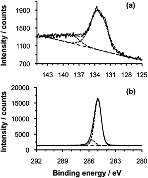 | ||
| Fig. 1 (a) P2p and (b) C1s regions of the XPS spectra of n-octadecylphosphonic acid monolayer on aluminium oxide. | ||
The feasibility of patterning alkylphosphonate SAMs by nanoshaving was examined. Because of the very strong bond known to exist between the alkylphosphonate and the oxide surface, it was necessary to employ substantial loads. Lines were traced across the samples using silicon (Tapping Mode) probes with large force constants (20 to 50 N m−1). The samples were then immersed in a solution of an adsorbate with a contrasting terminal group, and subsequently imaged in contact mode using friction force microscopy (FFM).55,56 FFM yields contrast differences for regions of the surface with different surface free energies;57–60 it was hypothesized that removal of a hydrophobic alkylphosphonate, and its replacement by an adsorbate with a polar tail group, would yield a local increase in the surface free energy and hence an increase in the friction force.
Nanoshaving was carried out with the probe operating in air. It was found that damage began to be observed at loads greater than 50 nN, but while adsorbates were displaced from the surface, lines fabricated at loads smaller than 400 nN were generally discontinuous, suggesting incomplete removal of material from the surface. In addition to the expected stability of the SAM, resulting from the strong interaction between the phosphonate and the oxide, the high roughness of aluminium oxide made patterning difficult at low loads. Fig. 2(a) and (b) show FFM images of structures formed in an ODPA on aluminium oxide surface by nanoshaving under a load of 630 nN. In Fig. 2(a) the sample was immersed in a 1 mM aqueous solution of 4-aminobutylphosphonic acid for 20 min, and in Fig. 2(b), the sample was immersed in a 1 mM solution of 16-phosphono-hexadecanoic acid in ethanol for 30 min. In both cases, the polar tail group of the second adsorbate gave clear contrast with the surrounding, low surface energy regions functionalized by ODPA in FFM images. Topographical images of nanolines exhibited no contrast, confirming that nanoshaving removed only the adsorbate, without damaging the substrate (for example, Fig. 2(c), which shows the same region imaged by FFM in Fig. 2(b)). However, it was found that clear, fully continuous lines were only observed for features formed using larger loads in the lithographic step, in excess of 1 μN (Fig. 2(d)). At lower loads it is possible that partial removal of the adsorbates occurs, in a process similar to that reported recently by Lee et al.61 An alternate explanation is provided by Liu and Salmeron who reported that lateral displacement of strongly bound molecules can be reversible;62 at lower loads, the adsorbates may be displaced laterally, causing disruption of monolayer order, without being completely removed from the shaved region. For thiol monolayers this process is reversible over a range of loads, between 20 and 200 nN. However, when the load is increased to more than 400 nN, adsorbates were removed from the SAM.
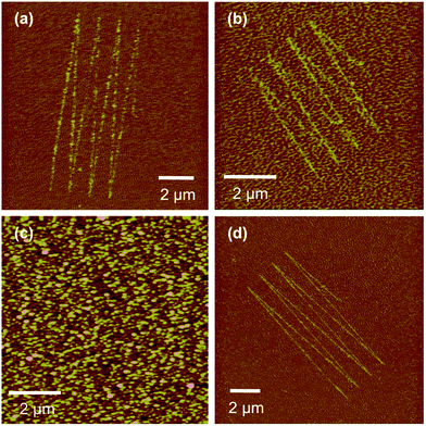 | ||
| Fig. 2 FFM images of structures fabricated by scratching in SAMs of ODPA on aluminium oxide at load forces (a and b) 630 nN and (d) 1.16 μN and subsequent immersion of the sample in 1 mM solutions of 4-aminobutylphosphonic acid (a and d) and 16-phosphono-hexadecanoic acid (b). (c) shows an AFM topographical image of the area shown in (b). | ||
In Fig. 2(d), nanoshaving was carried out at a load force of ca. 1.16 μN. This was sufficient to remove adsorbate molecules completely. The samples were immersed in a solution of polar 4-aminobutylphosphonic acid, giving rise to an increase in the surface free energy in regions where the hydrophobic ODPA had been replaced, and hence an increase in the friction force and bright contrast in the FFM image.
Nanoshaving is different from wear: in nanoshaving, the AFM tip makes a single sweep across the surface at a load force higher than the threshold for displacement of adsorbates, while wear is, in contrast, a process involving a reciprocating contact with the AFM tip and may occur at load forces less than this threshold. Therefore the load is the main factor for control of the tip–surface interaction in nanoshaving.
Fig. 3 shows AFM topographical images of nanostructures that were created by nanoshaving, under a load of 1 μN and ambient conditions, followed by immersion in an aqueous 1 mM solution of 4-aminobutylphosphonic acid for 20 min. Fig. 3(a) shows a lateral projection of a 4 × 4 μm2 region and demonstrates the formation of a series of parallel trenches. These trenches are narrow, with well-defined edges as is clearly apparent in Fig. 3(b), which shows two trenches at higher magnification. The line section in Fig. 3(c) shows the scale of one of these trenches. The full width at half maximum (FWHM) is 39 nm, and the depth is between 6 and 9 nm. These trenches appeared only after exposure of the sample to the aqueous solution of 4-aminobutylphosphonic acid, and they are attributed to etching of the aluminium oxide by the aqueous solution following displacement of the ODPA. While alkylphosphonate SAMs exhibit extremely high chemical stability under most conditions, they are susceptible to degradation under aqueous conditions and the aqueous solution of adsorbate is also able to etch the aluminium oxide film to some extent, yielding the topographical contrast shown in Fig. 3.
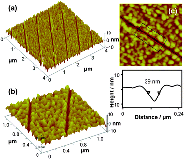 | ||
| Fig. 3 AFM topographical images of nanostructures formed by nanoshaving SAMs of ODPA under a load force of 1 μN followed by immersion in a 1 mM solution of 4-aminobutylphosphonic acid. | ||
Theoretically, the minimum width of trench is expected to be close to the tip diameter (ca. 20–25 nm).63 Nevertheless, in practice the line widths were typically larger than the tip diameter (hence the FWHM of 39 nm in Fig. 3).64 The shape of the tip is a significant factor determining pattern resolution, as the width of the patterned feature may be affected more by the shape of the tip than by the tip–surface contact size.64 Tip wear is also an important problem. The extent of wear during the shaving process was found to depend on the shape of the tip. To minimise problems due to tip wear, tips were replaced regularly.
The feasibility of using nanoshaving to form biological nanopatterns was examined. A SAM of [11-(4-azido-benzoylamino)-undecyl]-phosphonic acid was formed on the aluminium oxide surface. The aryl azide tail group will react with a primary amine under exposure to UV light leading to coupling of the amine to the surface. Selective removal of the photoactive azide by nanoshaving will enable regions to be defined that are free of the azide and which are thus not derivatised in the subsequent amine attachment step.
In order to pattern proteins, it is necessary to control non-specific adsorption, because proteins are adhesive molecules that bind strongly to many surfaces. The most widely used strategies for the control of non-specific adsorption rely upon the use of poly(ethylene glycol) and its derivatives. Oligo(ethylene glycol) functionalized SAMs have been found to exhibit exceptional resistance to protein adsorption. In the present study, PEG molecules with amine linkers were selected for photocoupling to the azide surface (see schematic diagram in Fig. 4(a)). Nanoshaving, with a load of 1.5 μN and a scan rate 1 μm s−1, was first used to remove azides selectively from regions of the surface. After nanoshaving, the sample was immersed in an aqueous solution of 4-aminobutyl phosphonic acid for 20 min leading to re-functionalisation of the exposed oxide surface. The PEG-NH2, in ethanolic solution, was then coupled to the azide in a photochemical process that involved exposure of the whole sample to UV light (λ = 325 nm) while immersed under the amine solution inside a quartz cell. Finally, the sample was immersed in a solution of 40 nm diameter NeutrAvidin-coated dye-loaded polymer nanoparticles in PBS buffer solution for 40 min, leading to adsorption of the NeutrAvidin particles on any regions not protected by coupling of the protein-resistant PEG-NH2. While this adsorbate consists of polymer nanospheres, they are coated with a monolayer of adsorbed protein and previous work indicates that they exhibit similar adhesive characteristics to proteins while offering brighter fluorescence than labelled proteins from the dye-loaded core. They are thus a more demanding test for resistance to non-specific adsorption.
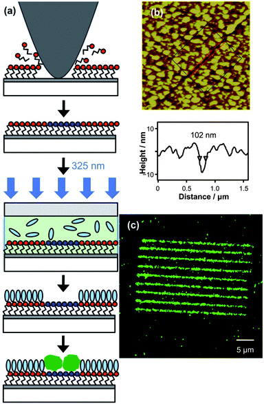 | ||
| Fig. 4 (a) Schematic diagram showing the fabrication process. Selective removal of the azide by nanoshaving is followed by adsorption of aminobutylphosphonic acid into the exposed areas, photochemical coupling of PEG-NH2 and then adsorption of NeutrAvidin particles. (b) 3.5 × 3.5 μm2 AFM topographical image of a single line in the resulting specimen, prior to adsorption of NeutrAvidin. (c) 40 × 40 μm2 confocal fluorescence microscopy image of nanopattern after adsorption of NeutrAvidin. | ||
Fig. 4(b) shows a nanoline prior to nanoparticle adsorption. The line section shows a FWHM of 102 nm, and a depth of ca. 10 nm. As noted above, the depth of the feature results not from the shaving process, but from a small amount of dissolution of the aluminium oxide during the adsorption of 4-aminobutyl phosphonic acid, and also the thickness of the PEG derivative. Fig. 4(c) shows a confocal fluorescence microscopy image of the same sample after adsorption of NeutrAvidin. The contrast between the nanolines and the surrounding surface is very good, indicating that there has been extensive adsorption of NeutrAvidin onto the lines, and that there is little adsorption of Neutravidin onto the surrounding surface, indicating that the PEG-functionalisation process was effective at inhibiting non-specific adsorption of protein.
The feasibility of using nanoshaved SAMs as resists for wet etching of aluminium was explored. An ODPA monolayer was used as the resist. Nanoshaving was carried out using a load of 600 nN and a scratching rate of 2 μm s−1. After modification, the sample was immersed in an aqueous solution of sodium hydroxide (0.4 mol dm−3) for 30 s.65 The aluminium surface was etched by sodium hydroxide in the scratched regions to create trenches 25–35 nm in depth and ca. 180 nm FWHM. The widths of the features were greater than the widths of the lines formed by the nanoshaving process, probably because the etch process is isotropic, leading to lateral erosion of Al as well as an increase in the depth of the feature. However, the features in Fig. 5 are sharp and well resolved.
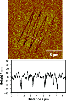 | ||
| Fig. 5 15 × 15 μm2 AFM topographical image and line section analysis of nanostructures formed by etching aluminium through nanoshaved SAMs of ODPA as the resist. | ||
Conclusions
SAMs of n-octadecylphosphonic acid on aluminium oxide surface have been patterned by nanoshaving under a load force between 400 nN and 1 μN and ambient conditions. Immersion of the samples in a solution of a second adsorbate leads to the functionalisation of the shaved regions with the second adsorbate yielding a chemical pattern. Protein-coated polymer nanoparticles have been immobilised on patterned SAMs on Al2O3 by nanoshaving a monolayer of [11-(4-azido-benzoylamino)-undecyl]-phosphonic acid and coupling the terminal azides of the remaining adsorbates to protein-resistant PEG-NH2. Using nanopatterned SAMs as a resist for etching by a solution of aqueous base leads to the transfer of patterns into the underlying metal film. Structures as narrow as 39 nm were fabricated under optimum conditions, suggesting that this approach is a promising one for modification of oxide surfaces. We believe that the capacity to chemically functionalize surfaces with varied terminal groups on the nanometre scale by this technique could be useful to development nanoelectronic devices, sensor technology and biological sciences.Acknowledgements
The authors thank EPSRC (grant EP/050271/1) for financial support.Notes and references
- G. Y. Liu, S. Xu and Y. L. Qian, Nanofabrication of self-assembled monolayers using scanning probe lithography, Acc. Chem. Res., 2000, 33, 457–466 CrossRef CAS PubMed.
- M. Woodson and J. Liu, Functional nanostructures from surface chemistry patterning, Phys. Chem. Chem. Phys., 2007, 9, 207–225 RSC.
- J. Sagiv, Organized monolayers by adsorption. 1. Formation and structure of oleophobic mixed monolayers on solid surfaces, J. Am. Chem. Soc., 1980, 102, 92–98 CrossRef CAS.
- L. Netzer and J. Sagiv, A new approach to construction of artificial monolayer assemblies, J. Am. Chem. Soc., 1983, 105, 674–676 CrossRef CAS.
- R. G. Nuzzo and D. L. Allara, Adsorption of bifunctional organic disulfides on gold surfaces, J. Am. Chem. Soc., 1983, 105, 4481–4483 CrossRef CAS.
- C. D. Bain, E. B. Troughton, Y.-T. Tao, J. Evall, G. M. Whitesides and R. G. Nuzzo, Formation of Monolayer Films by the Spontaneous Assembly of Organic Thiols from Solution onto Gold, J. Am. Chem. Soc., 1989, 111, 321–335 CrossRef CAS.
- J. C. Love, L. A. Estroff, J. K. Kriebel, R. G. Nuzzo and G. M. Whitesides, Self-Assembled Monolayers of Thiolates on Metals as a Form of Nanotechnology, Chem. Rev., 2005, 105, 1103–1170 CrossRef CAS PubMed.
- R. Maoz, S. R. Cohen and J. Sagiv, Nanoelectrochemical Patterning of Monolayer Surfaces: Toward Spatially Defined Self-Assembly of Nanostructures, Adv. Mater., 1999, 11, 55–61 CrossRef CAS.
- R. Maoz, E. Frydman, S. R. Cohen and J. Sagiv, Constructive Nanolithography: Site-Defined Silver Self-Assembly on Nanoelectrochemically Patterned Monolayer Surfaces, Adv. Mater., 2000, 12, 424–429 CrossRef CAS.
- S. Hoeppener, R. Maoz, S. R. Cohen, L. Chi, H. Fuchs and J. Sagiv, Constructive Nanolithography: Inert Monolayers as Patternable Templates for In-Situ Nanofabrication of Metal-Semiconductor-Organic Surface Structures – A Generic Approach, Adv. Mater., 2002, 14, 1036–1041 CrossRef CAS.
- S. Hoeppener, R. Maoz and J. Sagiv, Constructive Microlithography: Electrochemical Printing of Monolayer Template Patterns Extends Constructive Nanolithography to the Micrometer–Millimeter Dimension Range, Nano Lett., 2003, 3, 761–767 CrossRef CAS.
- S. Sun, K. S. L. Chong and G. J. Leggett, Nanoscale Molecular Patterns Fabricated by Using Scanning Near-Field Optical Lithography, J. Am. Chem. Soc., 2002, 124, 2414–2415 CrossRef CAS PubMed.
- G. J. Leggett, Light-directed nanosynthesis: near-field optical approaches to integration of the top-down and bottom-up fabrication paradigms, Nanoscale, 2012, 4, 1840–1855 RSC.
- S. Sun, M. Montague, K. Critchley, M.-S. Chen, W. J. Dressick, S. D. Evans and G. J. Leggett, Fabrication of Biological Nanostructures by Scanning Near-field Photolithography of Chloromethylphenylsiloxane Monolayers, Nano Lett., 2006, 6, 29–33 CrossRef CAS PubMed.
- S. A. Alang-Ahmad, L. S. Wong, E. ul-Haq, J. K. Hobbs, G. J. Leggett and J. Micklefield, Micrometer- and Nanometer-Scale Photopatterning Using 2-Nitrophenylpropyloxycarbonyl-Protected Aminosiloxane Monolayers, J. Am. Chem. Soc., 2009, 131, 1513–1522 CrossRef CAS PubMed.
- S. A. Alang Ahmad, L. S. Wong, E. ul-Haq, J. K. Hobbs, G. J. Leggett and J. Micklefield, Protein Micro- and Nanopatterning Using Aminosilanes with Protein-Resistant Photolabile Protecting Groups, J. Am. Chem. Soc., 2011, 133, 2749–2759 CrossRef CAS PubMed.
- M. Montague, R. E. Ducker, K. S. L. Chong, R. J. Manning, F. J. M. Rutten, M. C. Davies and G. J. Leggett, Fabrication of Biomolecular Nanostructures by Scanning Near-Field Photolithography of Oligo(ethylene glycol) Terminated Self-Assembled Monolayers, Langmuir, 2007, 23, 7328–7337 CrossRef CAS PubMed.
- N. P. Reynolds, S. J. Janusz, M. Escalante-Marun, J. Timney, R. E. Ducker, J. D. Olsen, C. Otto, V. Subramanian, G. J. Leggett and C. N. Hunter, Directed Formation of Micro- and Nanoscale Patterns of Functional Light Harvesting LH2 Complexes, J. Am. Chem. Soc., 2007, 129, 14625–14631 CrossRef CAS PubMed.
- N. P. Reynolds, J. D. Tucker, P. A. Davison, J. A. Timney, C. N. Hunter and G. J. Leggett, Site-Specific Immobilization and Micrometer and Nanometer Scale Photopatterning of Yellow Fluorescent Protein on Glass Surfaces, J. Am. Chem. Soc., 2009, 131, 896–897 CrossRef CAS PubMed.
- E. u. Haq, Z. Liu, Y. Zhang, S. A. A. Ahmad, L.-S. Wong, S. P. Armes, J. K. Hobbs, G. J. Leggett, J. Micklefield, C. J. Roberts and J. M. R. Weaver, Parallel Scanning Near-Field Photolithography: The Snomipede, Nano Lett., 2010, 10, 4375–4380 CrossRef PubMed.
- R. D. Piner, J. Zhu, F. Xu, S. Hong and C. A. Mirkin, Dip-pen nanolithography, Science, 1999, 283, 661–663 CrossRef CAS PubMed.
- S. Hong, J. Zhu and C. A. Mirkin, Multiple Ink Nanolithography: Toward a Multiple-Pen Nano-Plotter, Science, 1999, 286, 523–525 CrossRef CAS PubMed.
- K.-B. Lee, S.-J. Park, C. A. Mirkin, J. C. Smith and M. Mrksich, Protein Nanoarrays Generated by Dip-Pen Nanolithography, Science, 2002, 295, 1702–1705 CrossRef CAS PubMed.
- L. Demers, D. S. Ginger, S.-J. Park, Z. Li, S.-W. Chung and C. A. Mirkin, Direct Patterning of Modified Oligonucleotides on Metals and Insulators by Dip-Pen Nanolithography, Science, 2002, 296, 1836–1838 CrossRef CAS PubMed.
- Y. Li, B. W. Maynor and J. Liu, Electrochemical AFM dip-pen nanolithography, J. Am. Chem. Soc., 2001, 123, 2105–2106 CrossRef CAS PubMed.
- J. Hyun, S. J. Ahn, W. K. Lee, A. Chilkoti and S. Zauscher, Molecular Recognition-Mediated Fabrication of Protein Nanostructures by Dip-Pen Nanolithography, Nano Lett., 2002, 2, 1203–1207 CrossRef CAS.
- S. Hong and C. A. Mirkin, A Nanoplotter with Both Parallel and Serial Writing Capabilities, Science, 2000, 288, 1808–1811 CrossRef CAS PubMed.
- M. Zhang, D. Bullen, S. W. Chung, S. Hong, K. S. Ryu, Z. F. Fan, C. A. Mirkin and C. Liu, A MEMS nanoplotter with high-density parallel dip-pen manolithography probe arrays, Nanotechnology, 2002, 13, 212–217 CrossRef CAS.
- K. Salaita, Y. Wang, J. Fragala, R. A. Vega, C. Liu and C. A. Mirkin, Massively Parallel Dip-Pen Nanolithography with 55000-Pen Two-Dimensional Arrays, Angew. Chem., Int. Ed., 2006, 45, 7220–7223 CrossRef CAS PubMed.
- S. Xu and G. Y. Liu, Nanometer-scale fabrication by simultaneous nanoshaving and molecular self-assembly, Langmuir, 1997, 13, 127–129 CrossRef CAS.
- N. A. Amro, S. Xu and G.-Y. Liu, Patterning Surfaces Using Tip-Directed Displacement and Assembly, Langmuir, 2000, 16, 3006–3009 CrossRef CAS.
- G.-Y. Liu and N. A. Amro, Positioning Protein Molecules on Surfaces: A Nanoengineering Approach to Supramolecular Chemistry, Proc. Natl. Acad. Sci. U. S. A., 2002, 99, 5165–5170 CrossRef CAS PubMed.
- M. Liu, N. A. Amro, C. S. Chow and G.-Y. Liu, Production of Nanostructures on DNA Surfaces, Nano Lett., 2002, 2, 863–867 CrossRef CAS.
- D. Zhou, X. Wang, L. Birch, T. Rayment and C. Abell, AFM Study on Protein Immobilization on Charged Surfaces at the Nanoscale: Toward the Fabrication of Three-Dimensional Protein Nanostructures, Langmuir, 2003, 19, 10557–10562 CrossRef CAS.
- D. S. Zhou, K. Sinniah, C. Abell and T. Rayment, Label-Free Detection of DNA Hybridization at the Nanoscale: A Highly Sensitive and Selective Approach using Atomic Force Microscopy, Angew. Chem., Int. Ed., 2003, 42, 4934–4937 CrossRef CAS PubMed.
- M. Kaholek, W.-K. Lee, B. LaMattina, K. C. Caster and S. Zauscher, Fabrication of Stimulus-Responsive Nanopatterned Polymer Brushes by Scanning Probe Lithography, Nano Lett., 2004, 4, 373–376 CrossRef CAS.
- J. Shi, J. Chen and P. S. Cremer, Patterning of Supported Bilayers by Nanoshaving Lithography, J. Am. Chem. Soc., 2008, 130, 2718–2719 CrossRef CAS PubMed.
- M. Kaholek, W.-K. Lee, J. Feng, B. LaMattina, D. J. Dyer and S. Zauscher, Weak Polyelectrolyte Brush Arrays Fabricated by Combining Electron-Beam Lithography with Surface-Initiated Photopolymerization, Chem. Mater., 2006, 18, 3660–3664 CrossRef CAS.
- M. Textor, L. Ruiz, R. Hofer, A. Rossi, K. Feldman, G. Hahner and N. D. Spencer, Structural Chemistry of Self-Assembled Monolayers of Octadecylphosphonic Acid on Tantalum Oxide Surfaces, Langmuir, 2000, 16, 3257–3271 CrossRef CAS.
- S. Tosatti, R. Michel, M. Textor and N. D. Spencer, Self-Assembled Monolayers of Dodecyl and Hydroxy-dodecyl Phosphates on Both Smooth and Rough Titanium and Titanium Oxide Surfaces, Langmuir, 2002, 18, 3537–3548 CrossRef CAS.
- M. Zwahlen, S. Tosatti, M. Textor and G. Hahner, Orientation in Methyl- and Hydroxyl-Terminated Self-Assembled Alkanephosphate Monolayers on Titanium Oxide Surfaces Investigated with Soft X-Ray Absorption, Langmuir, 2002, 18, 3957–3962 CrossRef CAS.
- D. M. Spori, N. V. Venkataraman, S. G. P. Tosatti, F. Durmaz, N. D. Spencer and S. Zurcher, Influence of Alkyl Chain Length on Phosphate Self-Assembled Monolayers, Langmuir, 2007, 23, 8053–8060 CrossRef CAS PubMed.
- W. Gao, L. Dickinson, C. Grozinger, F. G. Morin and L. Reven, Self-Assembled Monolayers of Alkylphosphonic Acids on Metal Oxides, Langmuir, 1996, 12, 6429–6435 CrossRef CAS.
- R. D. Ramsier, P. N. Henriksen and A. N. Gent, Adsorption of Phosphorus Acids on Alumina, Surf. Sci., 1988, 203, 72–88 CrossRef CAS.
- L. H. Dubois and R. G. Nuzzo, Synthesis, Structure, and Properties of Model Organic Surfaces, Annu. Rev. Phys. Chem., 1992, 43, 437–463 CrossRef CAS.
- G. Cao, H.-G. Hong and T. E. Mallouk, Layered metal phosphates and phosphonates: from crystals to monolayers, Acc. Chem. Res., 1992, 25, 420–427 CrossRef CAS.
- H. Byrd, S. Whipps, J. K. Pike, J. Ma, S. E. Nagler and D. R. Talham, Role of the Template Layer in Organizing Self-Assembled Films: Zirconium Phosphonate Monolayers and Multilayers at a Langmuir–Blodgett Template, J. Am. Chem. Soc., 1994, 116, 295–301 CrossRef CAS.
- I. L. Liakos, E. McAlpine, X. Chen, R. Newman and M. R. Alexander, Assembly of octadecyl phosphonic acid on the α-Al2O3 (0001) surface of air annealed alumina: Evidence for termination dependent adsorption, Appl. Surf. Sci., 2008, 255, 3276–3282 CrossRef CAS.
- B. Torun, B. Ozkaya and G. Grundmeier, Atomic Force Microscopy (AFM)-Based Nanografting for the Study of Self-Assembled Monolayer Formation of Organophosphonic Acids on Al2O3 Single-Crystal Surfaces, Langmuir, 2012, 28, 6919–6927 CrossRef CAS PubMed.
- O. El Zubir, I. Barlow, E. Ul-Haq, H. A. Tajuddin, N. H. Williams and G. J. Leggett, Generic Methods for Micrometer- and Nanometer-Scale Surface Derivatization based on Photochemical Coupling of Primary Amines to Monolayers of Aryl Azides on Gold and Aluminum Oxide Surfaces, Langmuir, 2012, 29, 1083–1092 CrossRef PubMed.
- S. Sun and G. J. Leggett, Micrometer and Nanometer Scale Photopatterning of Self-Assembled Monolayers of Phosphonic Acids on Aluminum Oxide, Nano Lett., 2007, 7, 3753–3758 CrossRef CAS.
- H. Kim, P. E. Colavita, P. Paoprasert, P. Gopalan, T. F. Kuech and R. J. Hamers, Grafting of molecular layers to oxidized gallium nitride surfaces via phosphonic acid linkages, Surf. Sci., 2008, 602, 2382–2388 CrossRef CAS.
- H. Kim, P. E. Colavita, P. Paoprasert, P. Gopalan, T. F. Kuech and R. J. Hamers, Grafting of molecular layers to oxidized gallium nitride surfaces via phosphonic acid linkages, Surf. Sci., 2008, 602, 2382–2388 CrossRef CAS.
- T. T. Foster, M. R. Alexander, G. J. Leggett and E. McAlpine, Friction Force Microscopy of Alkylphosphonic Acid and Carboxylic Acids Adsorbed on the Native Oxide of Aluminum, Langmuir, 2006, 22, 9254–9259 CrossRef CAS PubMed.
- R. Overney and E. Meyer, Tribological investigations using friction force microscopy, MRS Bull., 1993, 26–34 CAS.
- R. W. Carpick and M. Salmeron, Scratching the Surface: Fundamental Investigations of Tribology with Atomic Force Microscopy, Chem. Rev., 1997, 97, 1163–1194 CrossRef CAS PubMed.
- C. D. Frisbie, L. F. Rozsnyai, A. Noy, M. S. Wrighton and C. M. Lieber, Functional Group Imaging by Chemical Force Microscopy, Science, 1994, 265, 2071–2074 CAS.
- J.-B. D. Green, M. T. McDermott, M. D. Porter and L. M. Siperko, Nanometer-Scale Mapping of Chemically Distinct Domains at Well-Defined Organic Interfaces Using Frictional Force Microscopy, J. Phys. Chem., 1995, 99, 10960–10965 CrossRef.
- N. J. Brewer, B. D. Beake and G. J. Leggett, Variation of Frictional Forces in Air with the Compositions of Heterogeneous Organic Surfaces, Langmuir, 2001, 16, 735–739 Search PubMed.
- T. J. Whittle and G. J. Leggett, Quantitative Kinetic Measurements of the Esterification of Self-Assembled Monolayers of Mercaptoundecanol by Trifluoroacetic Anhydride Using Friction Force Microscopy, Langmuir, 2009, 25, 9182–9188 CrossRef CAS PubMed.
- M. V. Lee, K. A. Nelson, L. Hutchins, H. A. Becerril, S. T. Cosby, J. C. Blood, D. R. Wheeler, R. C. Davis, A. T. Woolley, J. N. Harb and M. R. Linford, Nanografting of Silanes on Silicon Dioxide with Applications to DNA Localization and Copper Electroless Deposition, Chem. Mater., 2007, 19, 5052–5054 CrossRef CAS.
- G. Y. Liu and M. B. Salmeron, Reversible Displacement of Chemisorbed N-Alkanethiol Molecules on Au(111) Surface – an Atomic-Force Microscopy Study, Langmuir, 1994, 10, 367–370 CrossRef CAS.
- J. E. Headrick, M. Armstrong, J. Cratty, S. Hammond, B. A. Sheriff and C. L. Berrie, Nanoscale patterning of alkyl monolayers on silicon using the atomic force microscope, Langmuir, 2005, 21, 4117–4122 CrossRef CAS PubMed.
- I.-H. Sung and D.-E. Kim, Study on nanoscale abrasive interaction between nanoprobe and self-assembled molecular surface for probe-based nanolithography process, Ultramicroscopy, 2007, 107, 1–7 CrossRef CAS PubMed.
- S. Sun and G. J. Leggett, Micrometer and nanometer scale photopatterning of self-assembled monolayers of phosphonic acids on aluminum oxide, Nano Lett., 2007, 7, 3753–3758 CrossRef CAS.
| This journal is © The Royal Society of Chemistry 2013 |