 Open Access Article
 This Open Access Article is licensed under a Creative Commons Attribution-Non Commercial 3.0 Unported Licence
Free standing TiO2 nanotube array electrodes with an ultra-thin Al2O3 barrier layer and TiCl4 surface modification for highly efficient dye sensitized solar cells†
Xianfeng Gao, Dongsheng Guan, Jingwan Huo, Junhong Chen and Chris Yuan*
Department of Mechanical Engineering, University of Wisconsin-Milwaukee, 3200 North Cramer Street, Milwaukee, WI 53211, USA. E-mail: cyuan@uwm.edu; Fax: +1-414-229-6958; Tel: +1-414-229-5639
First published on 12th August 2013
Abstract
Dye sensitized solar cells were fabricated with free standing TiO2 nanotube (TNT) array films, which were prepared by template assisted atomic layer deposition (ALD) with precise wall thickness control. Efforts to improve the photovoltaic performance were made by using Al2O3 barrier layer coating in conjunction with TiCl4 surface modification. An Al2O3 thin layer was deposited on the TNT electrode by ALD to serve as the charge recombination barrier, but it suffers from the drawback of decreasing the photoelectron injection from dye into TiO2 when the barrier layer became too thick. With the TiCl4 treatment in combination with optimal thickness coating, this problem could be avoided. The co-surface treated electrode presents superior surface property with low recombination rate and good electron transport property. A high conversion efficiency of 8.62% is obtained, which is about 1.8 times that of the device without surface modifications.
Introduction
Dye sensitized solar cells (DSCs) are developed as a promising alternative to commercial solar cells with the advantages of low cost and ease of processing.1–3 In a DSC, visible light is absorbed by the dye molecules to generate excited electrons. Then the photoexcited electrons will inject into the conduction band of TiO2, which is followed by the subsequent regeneration of dye by the I/I3− redox couple. Conventional DSCs are typically fabricated with mesoporous nanocrystalline TiO2 electrodes which have large internal surface areas for absorbing light-sensitive dyes but have limited charge collection efficiency. To further improve the power conversion efficiency of DSCs, one dimensional nanostructures such as TiO2 nanotube (TNT) arrays were introduced to take advantage of their increased charge collection efficiency and light harvesting efficiency.4,5The superiority of one-dimensional nanostructures over planar geometries is that they can decouple the directions of light absorption and charge carrier collection,6–8 which means the possibility of providing a long dimension in the TNT length direction for light absorption as well as a short dimension in the TNT wall thickness direction for effective charge collection. Related studies are under wide investigation and shows that the solar cell efficiency could be improved by adjusting the geometry of the TNT.9–12 But the improvement of DSC power conversion efficiency requires not only to set up direct connection between the light-absorbing and charge-collecting geometry, but also to control the chemistry at the interface between the electrode and electrolyte. Charge recombination reaction of the injected electron with the oxidizing agent of the electrolyte is a deleterious loss pathway even in many planar solar cell devices,13,14 and such interface recombination generally dominates the performance of high aspect ratio electrodes such as TNT, due to the increased interfacial contact area relative to their projected geometric area for light absorption. Controlling the chemical properties of the surfaces and junctions of such one-dimensional systems as TiO2 nanotube arrays is therefore especially important.
To adjust the chemical properties of the electrode surface and suppress the charge recombination between the electrode and electrolyte, one method is to deposit large band gap semiconductor thin layers on the TiO2 surface, which act as barriers for the interfacial electron transfer.15–17 Several metal oxide materials, such as Al2O3,13,18,19 ZrO2,13 SiO2,13 and ZnO,16 have been studied as potential barrier materials. Among them, Al2O3 is considered most promising for retarding interfacial recombination losses under negative applied bias.13 It has been proved that the photoconversion efficiency of DSCs could be improved by up to 35% with a thin layer Al2O3 coating.17 However, previous investigations on the Al2O3 barrier layer were only on TiO2 nanocrystalline electrodes.17,19–21 It still remains a question if the Al2O3 coating has the same effect on interface recombination to TNT electrodes, considering its high aspect ratio structure and increased interface contact area.
Besides, TiCl4 treatment is also an effective method to improve the chemical properties of the TiO2 surface. With TiCl4 treatment, a TiO2 nanocrystal layer will grow epitaxially on the original surface of the TiO2 electrodes,22 which will help improve the DSC performance in two ways: first, the deposited nanoparticles will increase the active layer and fill some gaps that the dye molecules cannot reach, leading to enhanced dye loading and light absorption.23 More importantly, TiCl4 treatment will cause a downward shift of the conduction band edge of the TiO2, resulting in reduced charge recombination and improved charge injection into the TiO2, which will consequently increase the DSC current density and the power conversion efficiency.23 However, the combined effects of TiCl4 treatment on the TNT electrodes coated with Al2O3 were never investigated before. It is still a question whether the TiCl4 treatment and the Al2O3 barrier layer could work together to reduce the surface charge recombination within the DSC devices to produce high efficiency solar cell performance, while at the same time how to avoid the forward electron injection retarding effect caused by the barrier layer with an increased thickness. This investigation would have potential applications in controlling the surface property of solar cell electrodes resulting from a combined multi-layer surface structure of Al2O3 and TiCl4 materials.
In this work, Al2O3 barrier coating in conjunction with TiCl4 treatment was designed to modify the surface property of TNT electrodes simultaneously, expecting to accumulate their charge recombination suppression effects, but avoiding their possible disadvantages such as the photoinjection retarding effect caused by thick barrier layer deposition, so as to obtain a highly efficient DSC. Specifically free standing TiO2 nanotube arrays fabricated via a template assisted ALD method were used as the photoelectrode. To get the best performance with the combined modification, optimal thickness of the Al2O3 charge barrier layer was investigated by ALD with precise thickness control. The results indicate that the Al2O3 barrier layer and TiCl4 treatment have accumulated effects to reduce the recombination and improve the solar cell performance. A high power conversion efficiency of 8.62% is obtained, which is about 1.8 times that of the solar cell based on bare TNT electrodes. The demonstrated results indicate that the surface property of the electrode is crucial to solar cell performance and this study on TiO2 nanotube arrays offers a strategy toward optimizing the energy conversion efficiency in solar cells based on high aspect ratio materials.
Experimental
Free standing TiO2 nanotube membrane fabrication
The TiO2 nanotube membranes were fabricated through a template-assisted Atomic Layer Deposition (ALD) technique. Commercial AAO membranes with 200 nm pores (Anodisc, Whatman) were selected as the template. Briefly, the AAO template was attached on a Si substrate for ALD TiO2 deposition with diffusion mode. After deposition, the AAO/TiO2 membrane was annealed at 450 °C in an oxygen atmosphere for 2 hours for crystallization. To release the free-standing TNT array film, the annealed membrane was immersed into 1 M NaOH solution for 1 h and washed with DI water. The hexamethyldisilizane (HMDS) drying technique was used to protect the free-standing film.Surface treatment
Prior to dye adsorption, an Al2O3 barrier layer was deposited on the electrode with ALD. Trimethylaluminum (TMA) and water were the two precursors for the binary reaction at 200 °C using 8 s diffusion time and 8 s interval between the two pulses. The thickness of the barrier layer was controlled precisely by the deposition cycle. To prepare co-surface treatment samples, the electrode was processed with TiCl4 by immersing the TiO2 nanotube anode in 0.2 M TiCl4 aqueous solution in a sealed beaker and kept at 70 °C for 30 minutes before Al2O3 coating, followed by rinsing with ethanol and annealed at 450 °C for 30 minutes. During the surface treatment, the bare FTO surface, where no TiO2 electrode exists, was protected.TiO2 nanotube solar cell fabrication
The prepared free-standing TNT array film was then transferred to a fluorine-doped oxide (FTO) substrate with its original one dimensional structure retained. The FTO substrate was prepared by doctor blading of a thin layer TiO2 nanoparticle paste (Solaronix, Ti-Nanoxide HT). The electrode was sintered at 450 °C for 30 minutes. After surface treatment, the electrode was sensitized overnight in 0.5 mM (Bu4N)2-[Ru(4,4′-(COOH)-2,2′-bipyridine)2(NCS)2] (N719) in ethanol solution. A 50 μm thick Surlyn frame was sandwiched between the open-pore side of the membrane and a platinized FTO. The electrolyte, 50 mM iodide/triiodide in methoxypropionitrile, was injected from the side of the electrodes.Performance characterization
A Hitachi S-4800 scanning electron microscope (SEM) and a Hitachi H9000NAR transmission electron microscope (TEM) were used to characterize the morphology of the nanotubes. The TNTs were dispersed in ethanol and then placed onto a TEM grid. The composition of the obtained material was examined by Energy-dispersive X-ray spectroscopy (EDS) integrated with SEM and TEM. X-ray photoelectron spectroscopy (XPS) was performed using a HP 5950A XPS/ESCA Element and Chemical Analyzer. The C 1s peak from the adventitious carbon-based contaminant, with a binding energy of 284.8 eV, is used as the reference for calibration. The J–V properties of TiO2 nanotube based DSCs were then tested using a Keithley 2420 source meter under illumination of 100 mW cm−2 by an oriel solar simulator. Photovoltage decay measurements and electrochemical impedance spectroscopy (EIS) were performed using a CHI660D Electrochemical Analyzer. Dye loading was quantified with an Ocean Optics UV-VIS Spectrometer (SD2000 fiber optics) by measuring the absorbance of N719 desorbed from the electrode in 10 mM NaOH.Results and discussion
Al2O3 barrier layer deposition on TNT electrodes for charge recombination suppression
As a barrier layer between the porous electrode and dye/electrolyte, the Al2O3 film will not only suppress the charge recombination between the electrode and the electrolyte, but also restrain the electron injection from the dye to the electrode. Generally, a thicker Al2O3 barrier layer may result in a slower charge recombination rate but may reduce the forward charge injection at the same time. Therefore, an optimal thickness of the barrier layer should be pursued for improving the best performance of solar cells. Previous work based on TiO2 nanocrystalline solar cells showed discrepancies in the optimal thickness values. For instance, Lin et al. reported an optimal Al2O3 thickness around 0.1 nm, which improved the efficiency by 14%.20 However, another study by Ganapathy et al. showed that 2 nm Al2O3 is required to obtain the best efficiency.24 Similar values of 2–2.5 nm thickness were experimentally verified with an improvement of efficiency up to 35% through an Al2O3 coating formed by the sol–gel method.3 In theory the thicker barrier layers will lower the device performance since the rate of electron tunnelling from the dye to TiO2 decays exponentially with the barrier layer thickness.25 These discrepancies may be attributed to the difference in the Al2O3 deposition method and different surface properties of the photoelectrodes. Therefore, to obtain the best performance with combined surface treatment for the obtained TNT electrode, it is necessary to investigate the optimal thickness of the Al2O3 barrier layer first. With this purpose, a series of DSC samples with various thicknesses of Al2O3 barrier layers are fabricated, as controlled by ALD with different deposition cycles, at 1 cycle, 2 cycles, 5 cycles and 15 cycles.In the experiment, the TiO2 nanotube arrays were synthesized by AAO template assisted ALD followed by chemical etching to release TiO2 nanotube arrays from the template. The nanotube wall thickness is controlled around 23 nm for optimal performance, based on our previous study.26 Then the free-standing TiO2 nanotube film was transferred to FTO and made into a photoelectrode. An ultra-thin Al2O3 layer was deposited by ALD on the TiO2 electrode with precise thickness control before solar cell fabrication.
Fig. 1 shows the SEM and EDS mapping images of the TiO2 nanotube arrays after ALD coating. Fig. 1a is the top view of the nanotube arrays, which shows a compact tube structure. The average size of the nanopores is around 200 nm. The cross-sectional image of nanotube arrays is shown in the inset of Fig. 1a. The perfect vertically aligned tube structure will help the electron transportation inside the electrode. The length of the nanotube is around 40 μm. Fig. 1b is a cross-sectional image of both inner and outer surfaces of the nanotube, which shows that the deposition preserves the structure of the nanotube arrays quite well. To confirm the uniform coating of the Al2O3 deposition by ALD, EDS mapping was performed on an internal wall of the nanotube. As shown in the inset of Fig. 1b, Al element disperses uniformly along the tube surface, which suggests successful formation of a conformal coating on the surface of the nanotube wall.
 | ||
| Fig. 1 SEM and EDX mapping images show uniform coating. | ||
To investigate the detailed structure of the TiO2 nanotube after Al2O3 deposition, TEM was performed for a single TiO2 nanotube. Fig. 2a is a TEM image of the single nanotube after 15 cycle Al2O3 deposition, which shows a compact structure and uniform coating. A thin Al2O3 layer was coated on both inside and outside of the nanotube walls. EDS (Fig. 2b) is also performed focusing on single nanotubes, providing direct evidence of Al2O3 deposition. Fig. 2c and d are high magnification images of the TiO2 nanotube coated with Al2O3 at 5 and 15 ALD cycles, respectively. The images show obvious TiO2 thickness difference, suggesting a successful Al2O3 thickness control by ALD. The thickness is around 0.65 nm for 5 cycles and 1.8 nm for 15 cycles, yielding an average growth rate of ∼0.12 nm per cycle.
 | ||
| Fig. 2 TEM image (a) and EDS (b) of single Al2O3 coated TiO2 nanotubes. TEM images of the TiO2 nanotube wall coated with 5 cycles (c) and 15 cycles Al2O3 (d). | ||
XPS spectra of the Al2O3 coated TiO2 nanotube electrodes were recorded to confirm the interactions between the deposited Al2O3 and TiO2, as shown in Fig. 3. For the bare TiO2, the Ti 2p3/2 peak located at 459 eV (Table 1) lies within the range of 458.8–459.4 eV reported in the literature for TiO2.27-29 Following the ALD of the first Al2O3 coating, the binding energy of the Ti 2p3/2 peak was shifted from −0.1 to 458.9 eV; after 15 cycles Al2O3 coating, the binding energy was shifted further to 459.1 eV. These shifts of the Ti 2p3/2 peaks indicate an interfacial reaction existing within the 0.12 nm thickness of the Al2O3 layer, which also show the surface coverage change accordingly with the Al2O3 coating.29 The interfacial reaction can be seen more clearly in Al 2p spectra shown in Fig. 3b. The Al 2p peak of 1 cycle Al2O3 coated TiO2 electrodes located at 74.2 eV (Table 1) was identified as Al2O3 according to the published literature.28,29 This peak shifts to 74.5 eV after 15 cycles ALD coating. It is also noted that the intensity of Ti peaks decreases and that of the Al peak increases with the increased cycles of ALD. This intensity change is attributed to the increased Al2O3 coverage and thickness. Actually, the description of an ALD film as a conformal layer to estimate its thickness is inaccurate for ultra-thin films, especially for those ALD films deposited only by 1 and 2 cycles which actually consists of discontinuous Al2O3 monolayer stacks.29,30 Therefore, the surface coverage of TiO2 is increased with the increasing cycles and forms a continuous Al2O3 layer gradually, which would cause a related XPS intensity change of the Ti peak and the Al peak. The XPS spectra reflect a precise thickness control of Al2O3 coating, and the peak shifts indicate interface reaction after the Al2O3 doping, which would cause a band bending from the surface to the interface and induce a built-in potential accelerating the electron transport from the Al2O3 layer to the TiO2 electrode.31
 | ||
| Fig. 3 XPS spectra of Ti 2p3/2 and Al 2p peaks from the Al2O3 coated TNT electrodes. | ||
| Cycles | Ti binding energy (eV) | Al binding energy (eV) |
|---|---|---|
| 0 | 459 | — |
| 1 | 458.9 | 74.2 |
| 2 | 458.8 | 74.3 |
| 5 | 459 | 74.5 |
| 15 | 459.1 | 74.5 |
The photocurrent density–photovoltage (J–V) curves of the TNT-based DSCs with different Al2O3 coatings are shown in Fig. 4. Detailed photovoltaic parameters as a function of the coated Al2O3 thickness are summarized in Table 2. The performance of DSC based on the TNT film without Al2O3 barrier layer deposition was also listed for comparison.26 The data show that the efficiency of the DSC highly depends on the thickness of the deposited Al2O3 barrier layer. Our experimental results indicate that the optimal Al2O3 layer thickness is 0.12 nm for 1 cycle of ALD, which allows the surface modified TiO2 anode to present a photoconversion efficiency value of 5.75%. The result is over 20% higher than that of bare TiO2 nanotube based solar cells obtained with a 4.65% efficiency value. These results indicate that the Al2O3 barrier layer could be an effective method to improve the TNT based solar cell performance. When the Al2O3 film thickness increases, the photoconversion efficiency drops drastically. As shown in Table 2, the power conversion efficiency of the electrodes with more than 5 cycles Al2O3 coating is less than 1%. The results show that the power conversion efficiency is quite sensitive to the thickness of the barrier layer, and generally an ultra-thin layer is enough for improving the performance, which is consistent with previously reported results on TiO2 nanocrystalline film solar cells.18,20
 | ||
| Fig. 4 I–V performance of TiO2 nanotube based solar cells with Al2O3 coating of varied thickness. | ||
| Al2O3 ALD coating | VOC [V] | JSC [mA cm−2] | FF | η [%] |
|---|---|---|---|---|
| Bare TiO2 (ref. 26) | 0.69 | 9.51 | 0.71 | 4.65 |
| 0.12 nm (1 cycle) | 0.67 | 11.30 | 0.75 | 5.75 |
| 0.24 nm (2 cycles) | 0.64 | 8.54 | 0.74 | 4.07 |
| 0.60 nm (5 cycles) | 0.63 | 1.06 | 0.57 | 0.38 |
| 1.80 nm (15 cycles) | 0.59 | 0.68 | 0.39 | 0.16 |
To discuss the effects of Al2O3 coating on the performance of the solar cell, the main charge transfer processes at the TiO2/dye/electrolyte interfaces should be considered. In a typical DSC device, visible light is absorbed by the sensitizer dye first to generate photoexcited electrons, which will be injected into the conduction band of TiO2 from the excited state of the dye, following the subsequent regeneration of the dye by the I/I3− redox couple. The injected electrons may recombine with the oxidized dye molecules or with the oxidized redox couple. The latter reaction is thought to be particularly critical to device performance. With the Al2O3 coating on the TiO2 surface, recombination reaction of the injected electron with the oxidizing agent of the electrolyte can only be finished by tunneling through the insulator. Therefore, the deposited Al2O3 layers will act as barriers for the interfacial electron transfer and suppress recombination.17,18 However, thick layer Al2O3 coating will also suppress the total electron injection due to the Al2O3 induced weakening of electronic coupling between the dye and TiO2 as well as modification of the TiO2 electronic structure,14 which will decrease the photocurrent drastically when the barrier becomes too thick. As shown in Table 2, only the solar cell fabricated with one layer Al2O3 coated TiO2 demonstrates improved efficiency in comparison with the cell fabricated with TiO2 without Al2O3 coating. The optimal Al2O3 barrier layer thickness for the TNT electrode is 0.12 nm. It is worth noting that the optimal alumina thickness may vary with the deposition method. For an Al2O3 barrier layer formed with a sol–gel method, 2 nm conformal coating is still able to improve the efficiency of dye sensitized solar cells.17 The difference may be attributed to the fact that the liquid phase method, such as the surface sol–gel process, will result in an uneven coverage of the nanosized cavities of nanoporous TiO2 films because of incomplete penetration of the solution on the electrode surface.15
To investigate the recombination suppression effect of the Al2O3 barrier layer on TNT electrodes, photovoltage decay measurements were performed on the DSC device with bare TiO2 and Al2O3 coated TiO2 nanotubes at different ALD cycles (Fig. 5). As the rate of photovoltage decay is inversely proportional to the lifetime of photoelectron in DSCs, and the lifetime of electrons is further inversely proportional to the rate of recombination,32 a longer photovoltage decay time means that the electrons possess a slow recombination rate. The results show that the electrode with an Al2O3 barrier layer exhibits a longer photovoltage decay time than bare TiO2 (Fig. 5a), indicating the improved recombination characteristics with a longer electron lifetime. Also, the photovoltage decay time increases with Al2O3 thickness, which indicates that charge recombination suppression on the TiO2 surface strongly depends on the structure of the deposited Al2O3 film. Insight into the improvement of suppressing recombination may be obtained by investigating the charge carrier lifetime. Analysis of the photovoltage decay provides electron lifetimes (τn) related to the slope of the photovoltage vs. time plot by the expression32

 | ||
| Fig. 5 Measured photovoltage decay of DSCs with bare TNT and Al2O3 coated TNT electrodes. | ||
To characterize the effect of the Al2O3 coating on forward electron transfer from dye to TiO2, EIS of DSCs was carried out under AM1.5G illumination at bias of VOC and the frequency range from 0.1 Hz to 105 Hz with an AC amplitude of 10 mV. Fig. 6a shows the Nyquist plot of the TiO2 photoelectrodes coated with 1, 5, and 15 cycles of Al2O3. Impedance spectroscopy is a powerful technique to characterize the transport of electrons in DSCs. The Nyquist diagram features typically three semicircles that in the order of increasing frequency are attributed to the Nernst diffusion within the electrolyte, the electron transfer at the oxide/electrolyte interface, and the redox reaction at the platinum counter electrode.33,34 The middle frequency semicircle in the Nyquist plot reflects the property of photoinjected electrons within the TiO2.34 It is obvious that the charge transfer resistance increased rapidly with the increased Al2O3 layer thickness (Fig. 6). The reaction resistances of TiO2 covered with 1 cycle, 5 cycles and 15 cycles Al2O3 are 24.2 ohm, 245.9 ohm and 798.6 ohm respectively as analysed with Zview software. The large interface resistance with a thick Al2O3 covered TiO2 electrode results in much less electron injection and collection, and consequently a much lower photocurrent. Fig. 6b shows the Bode phase plots of the EIS results. As the peak frequency of the middle semicircle is inversely proportional to the lifetime of photoelectrons in a photoelectrode,34 the EIS results demonstrate that increasing the Al2O3 barrier layer from 1 cycle to 5 cycles to 15 cycles results in decreased peak frequency, indicating an increased photoelectron lifetime in the electrode with increased Al2O3 layer thickness. The results confirm that the Al2O3 barrier layer can act as an effective surface modification technique to help increase the electron lifetime within the TNT electrodes, although the interface resistance will be increased as well. It can be concluded that comparing the surface recombination improvement, the suppression effect of photoelectron injection dominates the interface reaction when the thickness is over 0.24 nm (2 layers). Therefore, to obtain the optimal photovoltaic performance of the device, the thickness of the Al2O3 barrier layer must be precisely controlled.
 | ||
| Fig. 6 Nyquist plots (a) and Bode plots (b) of electrochemical impedance spectra of Al2O3 coated TiO2 solar cells. | ||
In addition, the dye loadings on bare TNT electrodes and various Al2O3 coated TNT electrodes were also examined (Fig. S1†). The results show that the dye absorption of TNT electrodes was only slightly affected by the thickness of Al2O3, which is attributed to the minor surface area change resulting from ultra thin smooth Al2O3 layer coating. Accordingly, it is confirmed that the surface electric property plays an important role in adjusting the solar cell performance with ALD Al2O3 coated TNT electrodes, indicating that Al2O3 coating is an effective method to modify the surface property of TNT electrodes. Overall, the optimal thickness of the Al2O3 barrier layer for TNT electrodes is approximately 0.12 nm, which corresponds to 1 cycle ALD.
Improving the photovoltaic performance by combining the TiCl4 surface modification with Al2O3 barrier layer deposition
To further improve the efficiency of TiO2 nanotube based solar cells, co-surface treatment was designed to combine the optimal Al2O3 coating with TiCl4 surface treatment. Former discussions show that 1 cycle ALD coating provides the highest efficiency for TNT based solar cells, which balances the effect of charge recombination suppression and forward electron injection decreases at an optimal point. Therefore, 1 cycle ALD Al2O3 coating was conducted after the TNT electrode surface was treated with TiCl4 solution. For comparison, DSCs based on TiO2 nanotubes with only TiCl4 treatment was also fabricated and tested.Fig. 7 shows the comparison of the TNT surface before and after TiCl4 treatment. It is obvious that the TiCl4 treatment does not destroy the one dimensional tube structure of TNT and forms a nano-sized particle layer covering the TiO2 nanotube surface, which increases the active layer and leads to enhanced dye loading and light absorption.23 It has proved that TiCl4 treatment will also cause a downward shift of the conduction band edge of TiO2, resulting in reduced charge recombination and improved charge injection into TiO2, which consequently increase the short circuit current density (JSC) and the power conversion efficiency.23 Therefore, with TiCl4 treatment in conjunction with optimal Al2O3 barrier layer coating, it is expected that the recombination suppression effect can be accumulated without increasing the photoelectron injection resistance, and consequently get a higher photocurrent and power conversion efficiency.
 | ||
| Fig. 7 SEM images of the TNT wall before (a) and after (b) TiCl4 treatment. | ||
Fig. 8 shows TEM images of the 1 cycle ALD Al2O3 deposited on a TiCl4 treated TiO2 electrode. Fig. 8a is a low magnification image of single TiCl4 and Al2O3 co-treated nanotubes, which shows that TiO2 nanoparticles formed by TiCl4 treatment disperse on the TiO2 nanotube walls uniformly and generate a rough electrode surface. Although the ultra-thin layer Al2O3 is hardly separated from the substrate in the low magnification image, the EDS spectrum (inset of Fig. 8a) with a clear Al peak confirmed a successful Al2O3 deposition with 1 cycle ALD on TiCl4 treated TiO2 nanotube electrodes. The HRTEM image (Fig. 8b) provides a detailed surface morphology after 1 cycle Al2O3 deposition on TiCl4 treated TiO2 electrodes. It is observed that 1 cycle ALD Al2O3 deposition, actually only discontinuous Al2O3 islands cover the TiO2 surface, could be functional in improving the DSC device performance, with no obvious forward charge injection suppression but with efficient charge recombination reduction.
 | ||
| Fig. 8 TEM image (a) and HR-TEM (b) of the TNT wall after TiCl4 treatment with 1 cycle Al2O3 deposition. The inset shows the EDS spectrum of single TNT. | ||
Fig. 9 shows the comparison of I–V curves of solar cells treated with TiCl4 only and with TiCl4 in conjunction with Al2O3 deposition. With only TiCl4 treatment, the measured photocurrent is 12.9 mA cm−2 and a conversion efficiency of 6.77% is obtained. In the tests, the TiCl4 treatment enhanced the photocurrent of the DSC sample by over 30% when compared with the non-treated DSC. The enhanced result is consistent with other published work.35,36 For the DSC treated with TiCl4 in conjunction with an Al2O3 barrier layer, the measured photocurrent is 18.4 mA cm−2 and the increased power conversion efficiency is obtained at 8.62%, demonstrating a significant improvement of the conjunction effects from both TiCl4 and Al2O3. Detailed photovoltaic parameters are shown in Table 3.
 | ||
| Fig. 9 I–V performance of solar cells based on only TiCl4 treated and TiCl4–Al2O3 (1 cycle) co-treated TiO2 electrodes. | ||
| VOC [V] | JSC [mA cm−2] | FF | η [%] | |
|---|---|---|---|---|
| TiCl4 | 0.70 | 12.9 | 0.75 | 6.77 |
| TiCl4–Al2O3 | 0.66 | 18.4 | 0.71 | 8.62 |
To explain the mechanism of the co-surface treatment, photovoltage decay measurements were performed on the DSC devices with TiCl4 only treatment and with both TiCl4 and Al2O3 treatments to confirm the accumulated effect of the charge recombination properties, as shown in Fig. 10a. Fig. 10b shows the electron lifetime as a function of voltage. As shown in Fig. 10a, the TiCl4 treated TNT electrode (black curve) presents an obviously slower photovoltage decay time than the bare TNT electrode (Fig. 5a), suggesting that TiCl4 treatment has an obvious recombination suppression effect. Furthermore, the TiCl4 treated sample with 1 layer Al2O3 coating (red curve) appears to have a longer electron lifetime than that without Al2O3 coating, which indicates that the added Al2O3 coating can help reduce the recombination rate over the effect of TiCl4 treatment. Generally, the TiCl4 treatment and Al2O3 barrier layer coating hinder the electron recombination and prolong the electron lifetime with different mechanisms, which make it possible to obtain accumulated improvement for suppressing the surface recombination. TiCl4 treatment generates epitaxial growth of nanoparticles on the nanotube surface which will reduce nanotube surface impurities, defects and grain boundaries.37 The Al2O3 barrier layer covering the TiO2 nanoparticle formed by TiCl4 treatment will adjust the surface electric field and band edge, which reduces the surface recombination between the newly formed TiO2 nanoparticles and dye molecules.13 Therefore, the TNT electrode modified with an Al2O3 barrier layer in conjunction with TiCl4 treatment exhibits a lower recombination rate and longer electron lifetime than those of the samples modified just with a single method. The results proved that the combined surface treatment is an effective method to reduce the surface recombination and help increase the photocurrent.
 | ||
| Fig. 10 Photovoltage decay measurement of solar cells based on only TiCl4 treated and TiCl4–Al2O3 (1 cycle) co-treated TiO2 electrodes. | ||
Fig. 11a shows the Nyquist plot of the TiCl4 treated TNT photoelectrodes with and without Al2O3 coating. The results show that 1 layer Al2O3 coating on the electrode only slightly increases the charge transfer resistance. The resistance for TiCl4 treated TNT photoelectrodes with and without Al2O3 coating is 24.5 ohm and 22.3 ohm respectively, as extracted from the Nyquist plot. The low resistance values indicate that the forward electron injection from the dye molecule to the electrode is not suppressed by either of them. Actually, TiCl4 treatment will enhance the bonding between TiO2 and dye molecules, which facilitates the electron transfer and collection.37 As discussed before, the deposited ultra-thin Al2O3 layer (0.12 nm) only partially covered the TiO2 surface, which allows tunnelling of electron transfers and barely affects electron injections. Therefore, only a slight increase of resistance is observed after the thin layer Al2O3 coating. From the Bode plot in Fig. 11b, the EIS results show an obvious drop of the peak frequency of the middle semicircle after adding the 1 cycle ultra-thin Al2O3 barrier layer, which suggests an increased photoelectron lifetime of the co-surface treated device. The results are in good agreement with the previous photo-voltage decay measurement. Therefore, TiCl4 treatment and Al2O3 can work together to provide a better recombination suppression effect without restraining electron injection, and consequently increase the electron charge collection and produce large photocurrent.
 | ||
| Fig. 11 Nyquist plots (a) and Bode plots (b) of solar cells based on only TiCl4 treated and TiCl4–Al2O3 (1 cycle) co-treated TiO2 electrodes. | ||
Besides, it is believed that the TiO2 nanoparticle layer generated by TiCl4 treatment on the surface will increase the active surface of the electrode and load more dyes for enhancing the light absorption, and consequently contribute to the increase of photocurrent when compared with bare TNT electrodes. The dye loading enhancement was investigated with a TiO2 photoelectrode before and after TiCl4 treatment. Absorbance was measured after desorbing the absorbed dyes from the TNT electrode into NaOH solution, as shown in Fig. 12. The differences between the TiO2 with and without TiCl4 treatment are obvious. The peak intensity at 505 nm indicates an 8.6% higher dye loading for TiCl4-treated electrodes, which will contribute to the electron generation and thus improve the photocurrent. The slight peak position shift between different spectra may be attributed to the aggregation in higher concentration solution,38 which also indicates that the dye loading is strengthened with TiCl4 treatment.
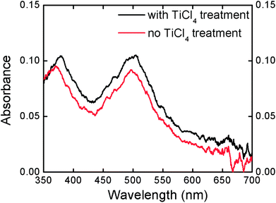 | ||
| Fig. 12 UV-Vis spectra of desorbed N719 from TiO2 electrodes with and without TiCl4 treatment. | ||
Overall, TiO2 nanotube electrodes modified with TiCl4 treatment in conjunction with an Al2O3 barrier layer present increased light absorption and prolonged electron lifetime without decreasing the photoelectron injection, resulting in enhanced photocurrent and high power conversion efficiency. The demonstrated results prove the importance of the surface property of the electrode and indicate that Al2O3 barrier layer deposition in conjunction with TiCl4 treatment is a promising method to improve the TNT electrode surface toward highly efficient DSCs.
Conclusions
In summary, TiO2 nanotube based electrodes were modified with an ALD Al2O3 barrier layer in conjunction with TiCl4 treatment for enhanced photovoltaic performance. The Al2O3 barrier layer suppresses the recombination between the injected electron and electrolyte, but it suffers from the drawback of inhibiting photoelectron injections from the dye molecules to the TiO2 electrode. This problem can be solved by combining the Al2O3 barrier layer with TiCl4 surface treatment. In our experiments, the TNT electrode with the co-surface treatment presents superior properties with an accumulated recombination suppression effect and unimpeded electron injection. The performance of the solar cells was improved significantly when compared with bare TNT based DSCs. A high power conversion efficiency of 8.62% is finally obtained. This work identified that surface treatment is extremely important to high aspect ratio TNT electrodes and the investigation identified a new way to optimize the DSC efficiency in future.Acknowledgements
The authors thank Dr Robertson Donald for assistance with TEM characterization and Steven E. Hardcastle for assistance with XPS characterization. The financial support from the Bradley Catalyst Program of the University of Wisconsin, Milwaukee, National Science Foundation (ECCS-1001039) and Department of Energy (DE-EE0003208) is gratefully acknowledged.Notes and references
- B. O'Regan and M. Gratzel, Nature, 1991, 353, 737–740 CrossRef CAS.
- L. Schmidt-Mende, U. Bach, R. Humphry-Baker, T. Horiuchi, H. Miura, S. Ito, S. Uchida and M. Grätzel, Adv. Mater., 2005, 17, 813–815 CrossRef CAS.
- J.-H. Yum, P. Walter, S. Huber, D. Rentsch, T. Geiger, F. Nüesch, F. De Angelis, M. Grätzel and M. K. Nazeeruddin, J. Am. Chem. Soc., 2007, 129, 10320–10321 CrossRef CAS PubMed.
- K. Zhu, N. R. Neale, A. Miedance and A. J. Frank, Nano Lett., 2007, 7, 69–74 CrossRef CAS PubMed.
- N. Wu, J. Wang, D. N. Tafen, H. Wang, J.-G. Zheng, J. P. Lewis, X. Liu, S. S. Leonard and A. Manivannan, J. Am. Chem. Soc., 2010, 132, 6679–6685 CrossRef CAS PubMed.
- S. U. M. Khan and T. Sultana, Sol. Energy Mater. Sol. Cells, 2003, 76, 211–221 CrossRef CAS.
- X. Feng, K. Shankar, O. K. Varghese, M. Paulose, T. J. Latempa and C. A. Grimes, Nano Lett., 2008, 8, 3781–3786 CrossRef CAS PubMed.
- K. Shankar, J. I. Basham, N. K. Allam, O. K. Varghese, G. K. Mor, X. Feng, M. Paulose, J. A. Seabold, K.-S. Choi and C. A. Grimes, J. Phys. Chem. C, 2009, 113, 6327–6359 CAS.
- D. Wang, L. Liu, F. Zhang, K. Tao, E. Pippel and K. Domen, Nano Lett., 2011, 11, 3649–3655 CrossRef CAS PubMed.
- X. Xu, X. Fang, T. Zhai, H. Zeng, B. Liu, X. Hu, Y. Bando and D. Golberg, Small, 2011, 7, 445–449 CrossRef CAS PubMed.
- H. Zhang, P. Liu, X. Liu, S. Zhang, X. Yao, T. An, R. Amal and H. Zhao, Langmuir, 2010, 26, 11226–11232 CrossRef CAS PubMed.
- Q. Zheng, H. Kang, J. Yun, J. Lee, J. H. Park and S. Baik, ACS Nano, 2011, 5, 5088–5093 CrossRef CAS PubMed.
- J. R. Durrant, S. A. Haque and E. Palomares, Coord. Chem. Rev., 2004, 248, 1247–1257 CrossRef CAS PubMed.
- L. J. Antila, M. J. Heikkilä, V. Aumanen, M. Kemell, P. Myllyperkiö, M. Leskelä and J. E. I. Korppi-Tommola, J. Phys. Chem. Lett., 2009, 1, 536–539 CrossRef.
- J. Guo, C. She and T. Lian, J. Phys. Chem. C, 2007, 111, 8979–8987 CAS.
- Y. Diamant, S. Chappel, S. G. Chen, O. Melamed and A. Zaban, Coord. Chem. Rev., 2004, 248, 1271–1276 CrossRef CAS PubMed.
- E. Palomares, J. N. Clifford, S. A. Haque, T. Lutz and J. R. Durrant, Chem. Commun., 2002, 1464–1465 RSC.
- E. Palomares, J. N. Clifford, S. A. Haque, T. Lutz and J. R. Durrant, J. Am. Chem. Soc., 2002, 125, 475–482 CrossRef PubMed.
- T. W. Hamann, O. K. Farha and J. T. Hupp, J. Phys. Chem. C, 2008, 112, 19756–19764 CAS.
- C. Lin, F.-Y. Tsai, M.-H. Lee, C.-H. Lee, T.-C. Tien, L.-P. Wang and S.-Y. Tsai, J. Mater. Chem., 2009, 19, 2999 RSC.
- M. Shanmugam, M. F. Baroughi and D. Galipeau, Thin Solid Films, 2010, 518, 2678–2682 CrossRef CAS PubMed.
- S. Kambe, S. Nakade, Y. Wada, T. Kitamura and S. Yanagida, J. Mater. Chem., 2002, 12, 723–728 RSC.
- P. M. Sommeling, B. C. O'Regan, R. R. Haswell, H. J. P. Smit, N. J. Bakker, J. J. T. Smits, J. M. Kroon and J. A. M. van Roosmalen, J. Phys. Chem. B, 2006, 110, 19191–19197 CrossRef CAS PubMed.
- V. Ganapathy, B. Karunagaran and S.-W. Rhee, J. Power Sources, 2010, 195, 5138–5143 CrossRef CAS PubMed.
- C. Prasittichai and J. T. Hupp, J. Phys. Chem. Lett., 2010, 1, 1611–1615 CrossRef CAS.
- X. Gao, J. Chen and C. Yuan, J. Power Sources, 2013, 240, 503–509 CrossRef CAS PubMed.
- G. Liu, W. Jaegermann, J. He, V. Sundström and L. Sun, J. Phys. Chem. B, 2002, 106, 5814–5819 CrossRef CAS.
- J. F. Moulder, W. F. Stickle, P. E. Sobol and K. D. Bomben, Handbook of X-ray Photoelectron Spectroscopy, Perkin-Elmer Press, Eden Prairie, 1962 Search PubMed.
- T.-C. Tien, F.-M. Pan, L.-P. Wang, F.-Y. Tsai and C. Lin, J. Phys. Chem. C, 2010, 114, 10048–10053 CAS.
- R. L. Puurunen, J. Appl. Phys., 2005, 97, 121301 CrossRef.
- T. C. Tien, F. M. Pan, L. P. Wang, C. H. Lee, Y. L. Tung, S. Y. Tsai, C. Lin, F. Y. Tsai and S. J. Chen, Nanotechnology, 2009, 20, 305201 CrossRef PubMed.
- A. Zaban, M. Greenshtein and J. Bisquert, ChemPhysChem, 2003, 4, 859–864 CrossRef CAS PubMed.
- Q. Wang, J. E. Moser and M. Gratzel, J. Phys. Chem. B, 2005, 109, 14945–14953 CrossRef CAS PubMed.
- R. Kern, R. Sastrawan, J. Ferber, R. Stangl and J. Luther, Electrochim. Acta, 2002, 47, 4213–4225 CrossRef CAS.
- G. K. Mor, K. Shankar, M. Paulose, O. K. Varghese and C. A. Grimes, Nano Lett., 2005, 6, 215–218 CrossRef PubMed.
- J. H. Park, T.-W. Lee and M. G. Kang, Chem. Commun., 2008, 2867–2869 RSC.
- B. C. O'Regan, J. R. Durrant, P. M. Sommeling and N. J. Bakker, J. Phys. Chem. C, 2007, 111, 14001–14010 CAS.
- E. Dell'Orto, L. Raimondo, A. Sassella and A. Abbotto, J. Mater. Chem., 2012, 22, 11364 RSC.
Footnote |
| † Electronic supplementary information (ESI) available: UV-Vis spectra of desorbed N719 dyes from TiO2 electrodes with and without Al2O3 barrier. See DOI: 10.1039/c3nr03198e |
| This journal is © The Royal Society of Chemistry 2013 |